1. Introduction
Terahertz (1–10 THz, and λ = 30–300 µm) frequencies are among the most underdeveloped electromagnetic spectra, even though their potential applications are promising, such as in the detection of chemical and biological agents, imaging for medical and security applications, astrophysics, remote sensing, non-invasive inspection, and free-space communication [
1]. This underdevelopment is mainly due to the lack of coherent compact THz sources that can provide high output power (greater than the mW level) at room temperature. Electronic devices on the microwave and millimeter-wave frequency side, such as transistors, Gunn diodes, Schottky-diode frequency multipliers, and photomixers, utilizing freely moving electrons, are limited by the transit time and parasitic RC time constants [
2]. As a result, the power level of these devices decreases rapidly as the frequency increases above 1 THz. Photonic devices based on interband transitions on the near-infrared and optical frequency side are limited to their energy gap, which is normally greater than 10 THz, even for narrow-gap lead-salt materials. These conventional semiconductor devices that have been well developed are no longer able to produce comparable power in this frequency range, leaving a “THz gap” of ~1–10 THz in the development of electromagnetic spectra.
In the meantime, quantum cascade lasers (QCLs) have gained tremendous development in the last two decades [
3]. Nowadays, it is becoming the leading laser source in the mid-infrared (mid-IR) frequency range, and has many applications in gas sensing, environmental monitoring, medical diagnosis, security, and defense [
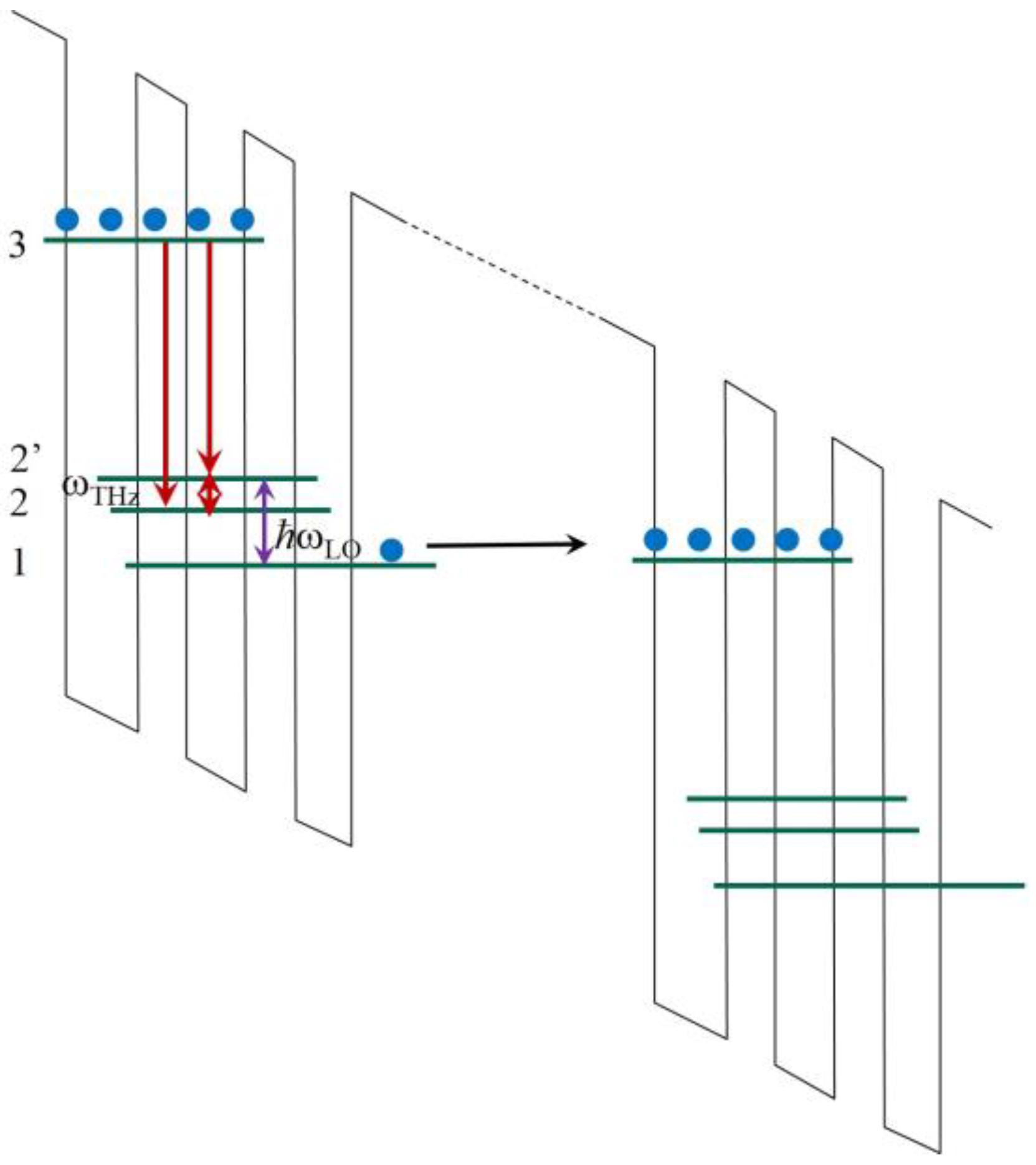
4]. The basic principle of QCL can be understood in
Figure 1. The electrons undergo optical transition between the two quantum states 3 and 2 and emit a photons with energy equal to the difference of the two, which is solely determined by the thickness of the wells and barriers and the conduction band offset [
5]. The population inversion is achieved by engineering a much shorter lifetime to the lower state 2 than the upper state 3 via a fast optical longitudinal (LO) phonon scattering to state 1. Large nonlinearities in quantum well structures originate from the interaction of the strongly-coupled quantum states. Among these, the nonlinear difference-frequency generation (DFG) [
6,
7] is of special interest due to its capability in producing THz emission.
When the lower level 2 is designed with a strong coupling with its neighboring level 2’, a large nonlinear susceptibility χ
(2) up to 10
4 pm/V will be created in the active region, which is more than two orders of magnitude higher than the nonlinear crystals. With the introduction of a dual wavelength operation with a certain THz frequency spacing, the THz emission is intracavity-generated via DFG [
6]. Unlike GaAs-based THz QCLs, which still need cryogenic cooling [
8,
9,
10,
11], the operating temperature of this type of THz source is only limited by the mid-IR QCLs which can reliably work at room temperature and above [
12]. In addition to providing a wealth of physics to study, this technique allows for compact, room-temperature operation over a wide spectral range. Utilizing state-of-the-art QCL technology, the THz sources based on DFG in QCLs is making steady progress, and are currently the only semiconductor sources that are able to emit multi-mW power and cover the entire 1–5 THz range at room temperature [
13]. In this paper, we present our recent breakthroughs in high-power and continuous-wave (CW) THz DFG QCLs, discussed in detail in the following sections, on nonlinear active region, composite DFB waveguide design, epi-down Čerenkov phase-matching scheme, high THz power operation up to the mW level, and room-temperature continuous-wave THz operation.
2. Design of the Nonlinear Active Region
For a mid-infrared (mid-IR) QCL featuring a large second-order nonlinear susceptibility (χ
(2)) for DFG in its active region and dual wavelength operation, THz emission can be generated from an extremely compact device at room temperature. The THz power strongly relies on high power from the mid-IR sources (
W1,
W2), and a large |χ
(2)|. A dual-core active region featuring double-phonon-resonance (DPR) and bound-to-continuum (BTC) depopulation schemes, has been used for the first generation of THz sources based on DFG QCLs [
6,
14,
15]. Among the two core designs, only the BTC core is designed with a giant nonlinear susceptibility and the DPR core merely acts as a mid-IR source with little THz generation. Meanwhile, the mid-IR QCL technology has made tremendous progress in power and efficiency, thanks to the improved material quality, waveguide, and especially the elaborate quantum designs [
16,
17,
18,
19]. Out of these, QCLs based on the single-phonon-resonance (SPR) design have demonstrated the highest power and efficiency in the shorter mid-IR wavelength range (4–6 µm) [
20]. The strong coupling of the lower lasing state and the upper injector state indicates that the SPR design in the long mid-IR wavelength range can be designed with giant nonlinearity without much compromise on its high power feature [
21].
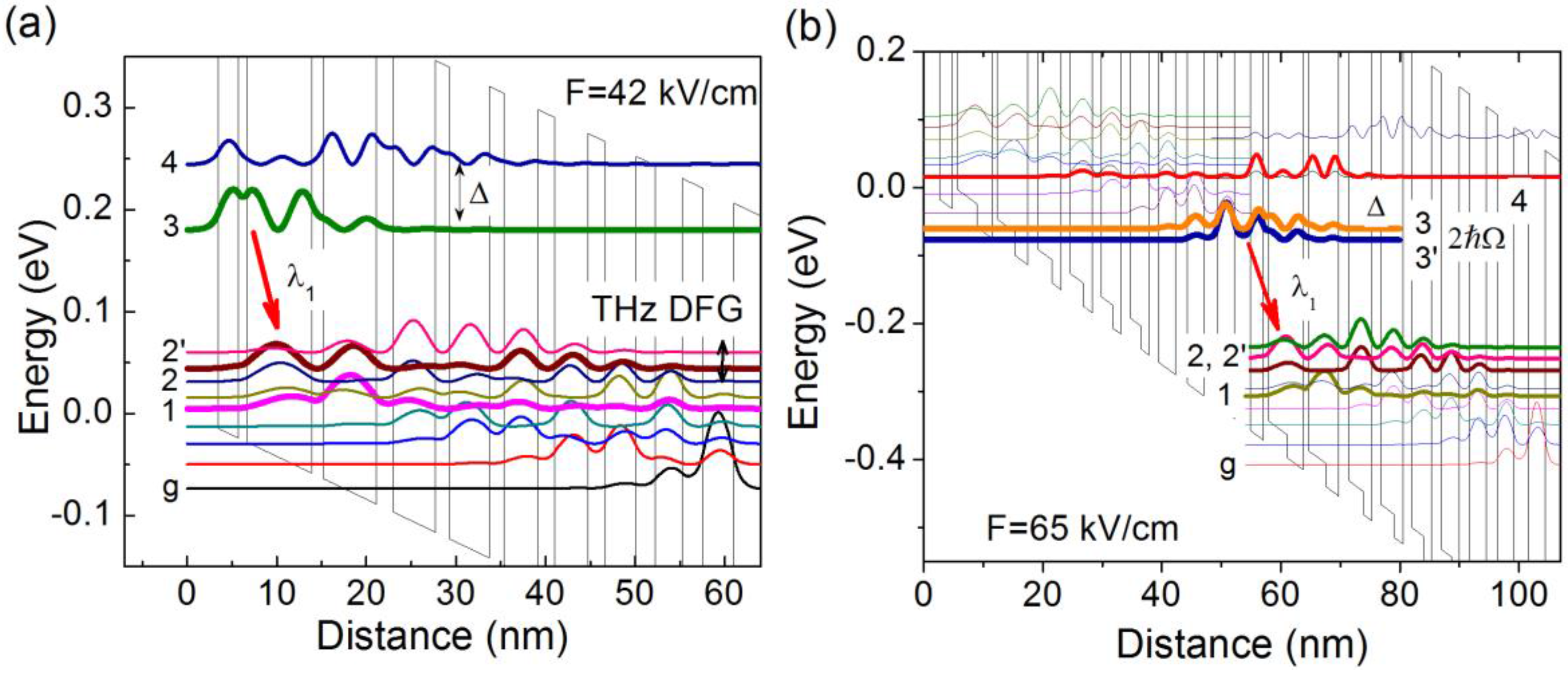
Figure 2a shows a lattice-matched Ga
0.47In
0.53As/Al
0.48In
0.52As SPR structure at a wavelength of λ
1 ~ 9.0 μm designed for THz DFG. The band structure is shown at the high fields when the maximum mid-IR powers are expected. The state 1 is separated by about one optical-phonon energy from state 2, which helps to depopulate state 2 with ultrafast optical-phonon scattering. Compared with the BTC structure in [
14] near the roll-over voltage, using the same simulation parameters, the lifetime of the upper lasing state 3 caused by phonon scattering is increased from 0.39 ps for the BTC design to 0.46 ps for the SPR design, while the lifetime of the lower lasing state 2 is maintained at 0.1 ps. The major contributions to the THz DFG nonlinearity stem from the adjacent state 2’ that is within 10–20 meV of the lower lasing state 2. The electron density in the states involved in DFG can be estimated with a simplified rate equation model by applying the lasing threshold condition (
Ggain = (α
m + α
w)/Г) at which the champing occurs.
Ggain, α
m, α
w, and Г are gain, mirror loss, waveguide loss, and confinement factor, respectively. Given the waveguide loss of 8 cm
−1, mirror loss 2.3 cm
−1 for a 3-mm long HR-coated cavity, and confinement factor of 0.4, the electron densities in the upper lasing level, the lower lasing level 2, and its adjacent levels contributing to DFG are calculated as 2.0 × 10
15, 2.1 × 10
14, 1.1 × 10
14, and 4 × 10
14 cm
−3, respectively. The nonlinear susceptibility is estimated to be |χ
(2)| = 3.97 × 10
4 pm/V at 4 THz.
The limited conduction band offset (~0.5 eV) for the lattice-matched design results in an energy spacing of ~240 meV between the upper laser level and the continuum states located above the barriers, which is not able to confine the electrons in the upper laser level effectively, and induces significant thermally-activated carrier leakage into the continuum. This leads to less efficient performance of the devices compared to the state-of-art shorter-wavelength counterparts. To further improve the THz performance, a nonlinear SPR active region based on the strain-balanced Al
0.63In
0.37As/Ga
0.35In
0.65As/ Ga
0.47In
0.53As material system is designed [
22]. The band structure is shown in
Figure 2b. The targeted wavelength is λ ~ 7.8 µm. The inserted Ga
0.47In
0.53As layers are used to balance the material strain within one stage. The conduction band offset is enhanced to ~0.74 eV. In the present strain-balanced design with a diagonal optical transition scheme, the increased conduction-band offset and interface roughness increases the broadening the oscillation linewidth to ~15–20 meV, compared to that of ~10 meV for the lattice-matched active region design [
21]. This allows for a stronger coupling design between the injector and upper lasing level. A high coupling strength with an energy splitting of 2 ħΩ = 16.5 meV is calculated for the present structure. This strong-coupling design not only effectively improves the carrier tunneling rate into the upper lasing state 3 [
23], but also enhances the DFG nonlinear susceptibility χ
(2). Normally, the optical nonlinearity is engineered by the adjusting the injector barrier thickness so that the lower laser state 2 couples with its neighboring level 2’ with an energy spacing of 14–17 meV (3.4–4.1 THz). Here, the strongly-coupling design, with an energy splitting of 16.5 meV, provides another scheme to the total nonlinear susceptibility. Given a threshold gain
gth = 5 cm
−1 for CW operation, a total nonlinear susceptibility of |χ
(2)| = 2.0 × 10
4 is obtained from the present design. This is comparable to the value of 2.6 × 10
4 pm/V from the previous lattice-matched active region design at λ ~ 9 µm with a higher threshold gain [
24].
3. Composite DFB Waveguide and Epi-Down Čerenkov Phase Matching Scheme
In a typical multimode Fabry-Pérot (FP) cavity, the light intensity spreads out among different mid-IR frequencies, and the total power is the sum over many small
Wi components. As such, the product
WiWj will be small and the THz spectrum will be rather broad (Δ
v ~ 0.5–1 THz). In order to purify and tune the THz spectrum, all the mid-IR power needs to be concentrated on the two mid-IR frequencies with single mode operation, and their frequency positions need to be controllable and tunable. The most straightforward way to this end is to use the composite DFB grating with wavelength components to purify and tune the mid-IR spectra [
15]. While the design strategy of dual-period DFB grating shares some similarity to the single-period DFB, like sufficient coupling strength for single mode operation, balancing the coupling strength, waveguide loss, and modal gain of the two grating components is of special importance.
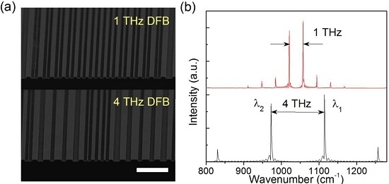
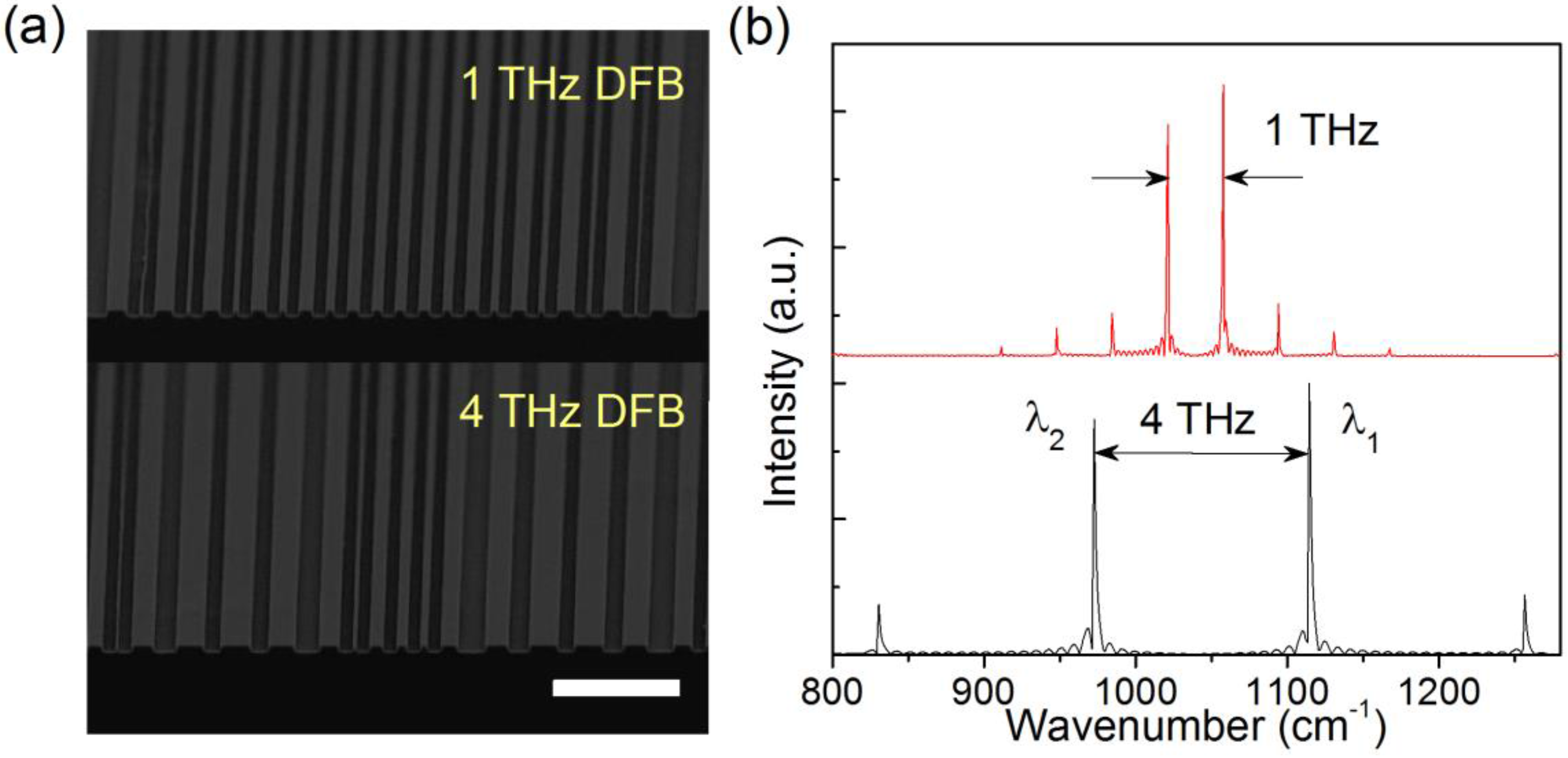
Figure 3a shows the scanning electron microscope (SEM) pictures for two composite DFB gratings designed for 1 THz and 4 THz, respectively. Double-exposure holographic lithography or electron-beam lithography have been used [
15,
21]. The exposing dose ratio between the two exposures is adjusted to balance the coupling coefficients (κ
1 for λ
1 and κ
2 for λ
2) and reflection intensity between the two wavelength components. As shown in
Figure 3b, roughly similar intensity is obtained by using the same exposure doses for the double e-beam exposure, which naturally balances the coupling strengths for the two wavelengths via their different grating duty cycles due to the different period components. Around a surface grating depth of 200 nm, similar coupling coefficients of ~10 cm
−1 are obtained for the two wavelengths. This grating design offers sufficient coupling strength for 2–3 mm cavities with high-reflection (HR) coatings.
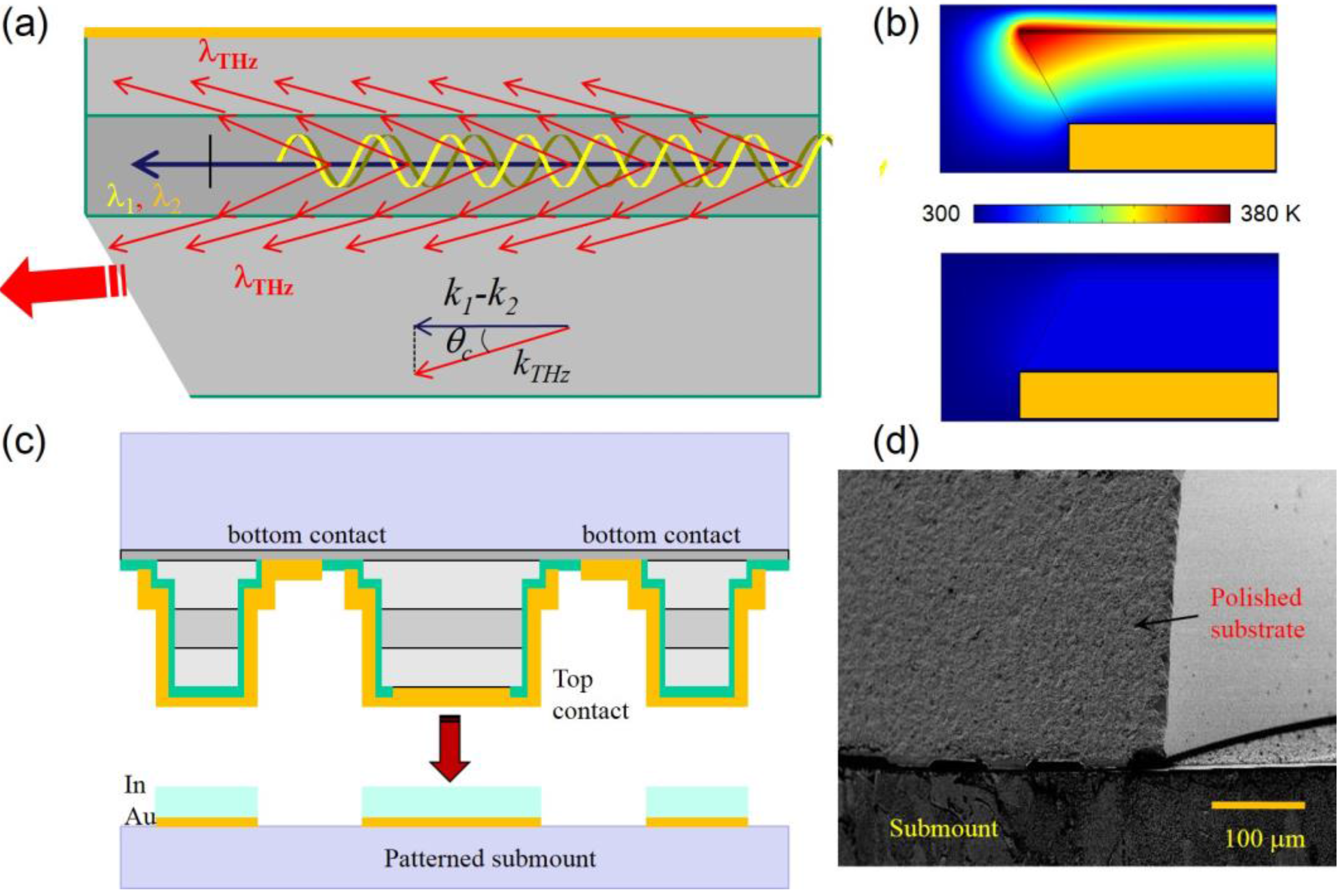
To achieve a high mid-IR-to-THz power conversion efficiency, the phase mismatching should be close to zero to obtain an effective nonlinear interaction. In a waveguide with a modal phase matching scheme, due to a faster frequency-dependent effective index in the THz range with respect to the mid-IR index (
nmid-IR), the modal phase matching is only satisfied within a relatively narrow frequency range for a certain waveguide [
25]. In contrast to this narrow-band phase-matching scheme, the Čerenkov scheme [
26] has been used as an effective broad-band phase matching method for THz generation in the externally-pumped optical rectification or DFG setups [
27]. Čerenkov nonlinear emission occurs when the nonlinear polarization wave propagates at a higher phase velocity compared to that of the nonlinear radiation, as shown in
Figure 4a. For THz DFG in QCLs, the waveguide for Čerenkov phase matching scheme can be designed so that the THz refractive index (
nTHz) in the QCL substrate is higher than the mid-IR group effective refractive index (
nmid-IR). In this case, the fundamental mid-IR wave propagates faster than the second-order DFG THz wave, and the THz wave travels at an angle
θC = cos
−1(
nmid-IR/
nTHz) with respect to the mid-IR wave,
θC is the Čerenkov angle. This can be achieved by replacing the n-doped InP substrate with a semi-insulating InP substrate, where
nTHz (~3.47–3.71) larger than
nmid-IR (~3.35) is fulfilled automatically in the 1–6 THz range. This broadband Čerenkov phase-matching scheme is used to take full advantage of the wide bandwidth of the THz nonlinear medium based on SPR design. The QCL epilayer structure, together with a 200-nm InGaAs bottom contact layer, are grown by gas-source molecular beam epitaxy on a semi-insulating InP substrate. The sample was processed into a ridge waveguide by dry or wet etching with a ridge width of 20–25 µm. The front facet is polished into 30° to facilitate the Čerenkov THz output.
Since the THz light is coupled out from the substrate with a facet-polished angle of 20–30° for Čerenkov phase matching scheme, the ideal scenario is to use a thick substrate to couple out as much light as possible. In the experiments, the 350 µm thick substrate is normally not polished, however, thick substrate will lead to inefficient heat removal in the epilayer-up mounting scheme, and a less efficient current injection scheme due to the single-side current injection through a thin layer of bottom contact. This results in the limited THz power output in spite of the relatively high power conversion efficiency [
21,
28].
Figure 4b (upper) show the temperature distributions of an epilayer-up mounted QCL with an asymmetric contact pattern near the front facet. The polished angle of the facet is set to be 30°. Clearly, the epilayer-up mounted Čerenkov device suffers severely from thermal and electrical issues, as the heat near the front facet is not effectively dissipated. Moreover, the non-uniform electrical distribution across the active region induces non-uniform current injection with the electrical field varying over 2–4 kV/cm. To address these two issues, double-sided current injection and epilayer-down mounting on a patterned submount are proposed [
29], as shown
Figure 4c. The heat dissipation is improved significantly as shown in
Figure 4c (lower), and the electrical distribution is much more uniform with electrical field variation less than 0.5 kV/cm in the lateral plane of the active region. In the experiment, AlN or diamond submounts are prepared with the patterns corresponding the contacts of the device for epi-down bonding.
Figure 4d is a SEM image of an epi-down mounted Čerenkov THz device.
4. High Power DFG QCL THz Sources
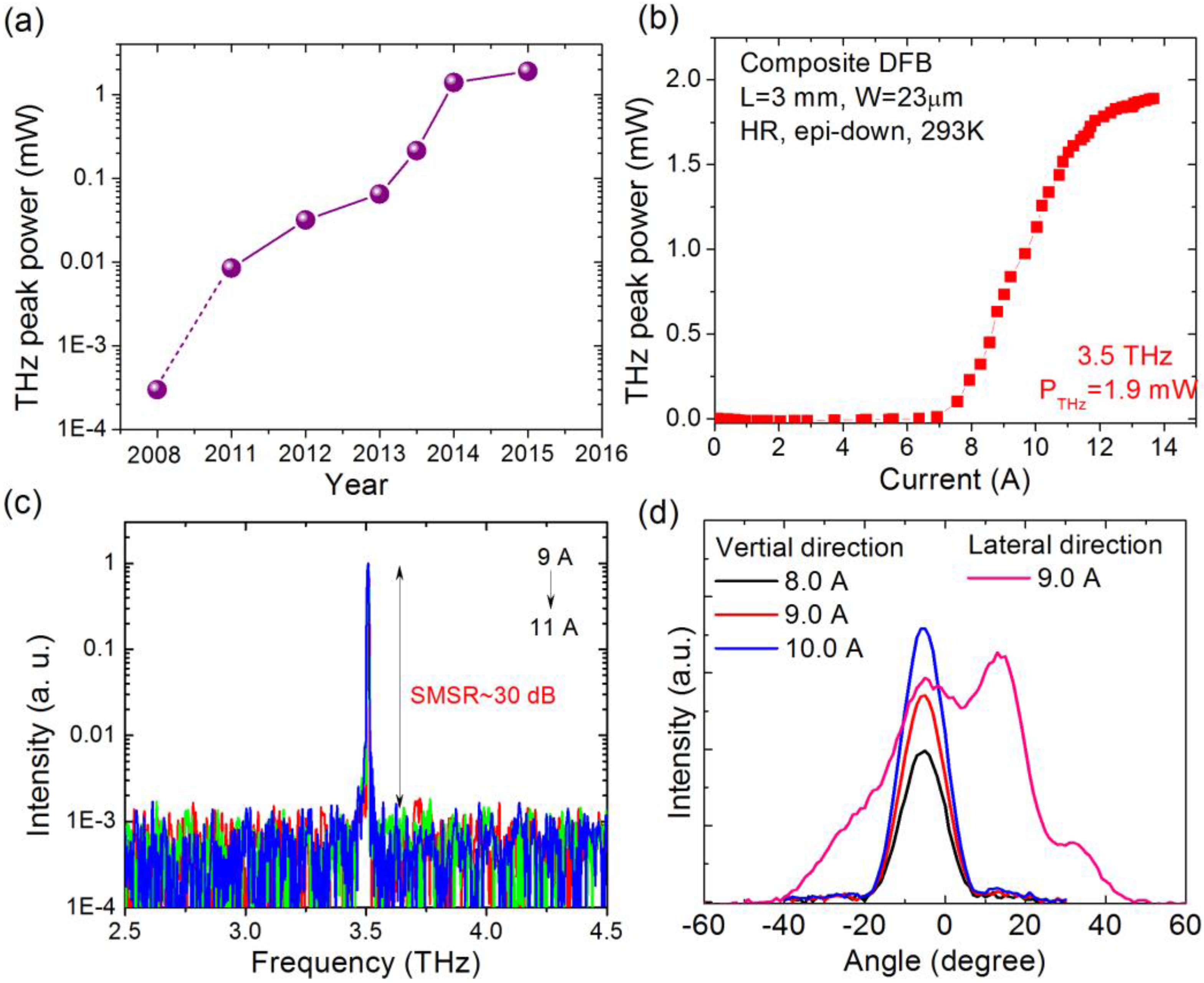
Ever since from the first demonstration, THz sources based on DFG QCLs have strived for high-power operation at room temperature. Through the above systematic optimizations to the nonlinear active region, DFB waveguide, phase matching scheme, and device bonding technique, the THz output power has experienced an exponential increase in recent years, as depicted in
Figure 5a. Currently, the highest THz power up to 1.9 mW with a conversion efficiency of 0.8 mW/W
2 is achieved from an HR-coated, 3-mm long, 23-µm wide, composited DFB laser epilayer-down mounted a patterned diamond submount, as shown in
Figure 5b. The measured THz power is not corrected with any collection efficiency. The maximum THz power wall plug efficiency for this device reaches 0.7 × 10
−3%.
Spectral emission is single mode at 3.5 THz with a side-mode suppression ratio (SMSR) as high as 30 dB, as shown in
Figure 5b. The far field testing indicates that the device exhibits a good beam profile with divergence angles of 12.5° in the vertical direction and 36° in the lateral direction with a dual-peak distribution. Ideally, the far field pattern of the Čerenkov THz emission inside of the QCL waveguide should be a conical shape with the cone angle equal to the Čerenkov angle because of the much longer emitting wavelength with respect to the width of the QCL waveguide [
24]. This indicates that only part of this radiation cone is able to be coupled out through the polished substrate facet limited by the Brewster’s angle θ
B ≈ ±16.5°, which is inferred from
θB = sin
−1(
nair/
nInP) with
nair = 1, and
nInP = 3.5. Considering another 30% reflection to both the mid-IR and THz emissions, the outcoupling efficiency of the emitted THz power with respect to the generated power is as low as 15%. Given the maximum recorded 1.9 mW output power, the total generated THz power in that device is estimated to be ~12 mW. Therefore, there is significant potential for THz power enhancement when an efficient THz outcoupler is applied to the THz waveguide. By enlarging the outcoupling aperture with a Si prism to allow for more THz light to be coupled out from the substrate or extract the THz light from the entire cavity via diffraction grating [
30], even higher THz power and efficiency in a wider spectral range in pulsed and CW modes can be obtained. This is of special importance to high THz frequency generation (>4.5 THz) where the phonon absorption in the semi-insulating InP substrate plays a leading role to the THz absorption prior to outcoupling. On the other hand, the power of a mid-IR QCL has been scaled up to 200 W [
31] and, with a similar strategy, the THz power can be further enhanced to tens of mW by scaling the device area.
5. Room Temperature Continuous Wave THz DFG QCL Sources
While a lot of effort has been devoted to improve the THz power [
24] and frequency tuning range of the THz sources based on DFG in QCLs [
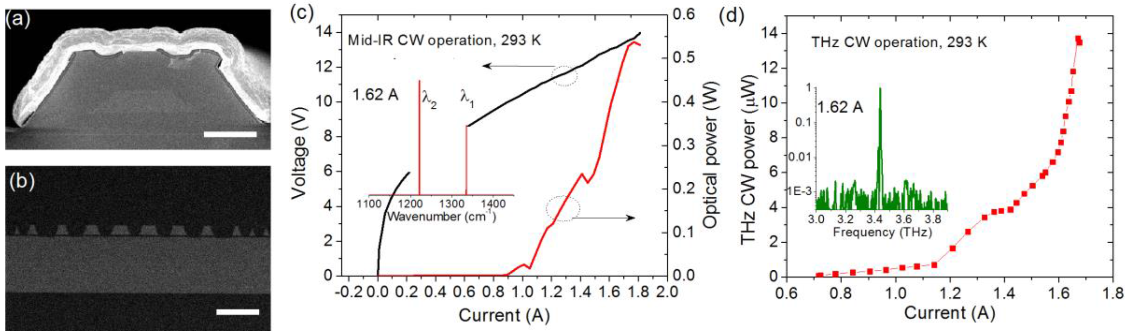
32], the capability of CW operation at room temperature is of significant importance to wide application and commercialization. Nevertheless, room temperature CW operation has been difficult to be achieved for the following reasons. First, the design priority has been to achieve a large nonlinear susceptibility for THz generation. However, this may compromise the mid-IR performance. Second, in order to obtain a large population inversion, the doping of the structure is much higher than a typical mid-IR QCL, which results in a high threshold current density, precluding room temperature CW operation. Third, in order to obtain high peak power, the waveguide structure is often wider than a typical mid-IR QCL, which poses a large challenge for thermal management. These issues are recently addressed by utilizing a low-loss buried-ridge waveguide design and highly dissipative epi-down mounting scheme (
Figure 6a), room-temperature continuous-wave (RT-CW) operation at 3.6 THz was demonstrated with a continuous power of 3 µW [
24].
To further enhance the THz CW power, a new strongly-coupled strain-balanced quantum cascade laser design for efficient THz generation based on intracavity DFG with an epi-down mounting scheme is presented. A single-phonon resonance active region made from a composite strain-balanced Al
0.63In
0.37As/Ga
0.35In
0.65As/Ga
0.47In
0.53As active region is designed with strong coupling of 2 ħΩ = 16.5 meV. The concurrent advantage of this strong coupling design is that the upper laser level spreads more into the injector region because of the thin injection barrier, so that the radiative transition is more diagonal, which increases not only the slope efficiency with elevated upper laser level lifetime, but also the gain spectral width, as evidenced by the electroluminescence (EL) measurement results [
22]. The FWHM of 380 cm
−1 is even broader than the previous dual-core lattice-matched active region with a FWHM of ~330 cm
−1 in the 9–11 µm wavelength range [
21], which makes this homogenous active region able to provide a sufficiently wide gain to support the 1–5 THz emission.
In CW operations, a 4-mm long composite DFB device emits up to 0.53 W with threshold current densities of 1.87 kA/cm
2, as shown in
Figure 6b. The inset is the CW lasing spectrum at 1.62 A. Stable dual-wavelength operation at λ
1 = 7.46 µm and λ
2 = 8.15 µm with a frequency spacing of 3.4 THz is observed. For an FP device with identical geometry, a maximum power of 3 W and threshold current density of 1.95 kA/cm
2 in pulsed mode operation, and a maximum power of 1.1 W and a threshold current density of 2.2 kA/cm
2 in CW operation are demonstrated, respectively. The maximum wall plug efficiencies (WPEs) are 10% and 4% for pulsed mode and CW operations, respectively.
Figure 6c is the THz power of the composite DFB QCL in CW operations at 293 K. Maximum CW power of 14 µW with conversion efficiencies of η = 0.35 mW/W
2, and THz WPEs of 0.8 × 10
−6 is obtained. The superlinear increase in CW THz power in
Figure 6c is due to the rapid power increase in λ
1 and dramatic power balancing between λ
1 and λ
2 in the current range of 1.45–1.68 A. The maximum CW powers are much higher than previous demonstrations in [
24], despite that the conversion efficiency being lower due to the relatively lower nonlinearity induced by the reduced threshold gain. As a result, the THz CW WPE is about one order of magnitude higher than the previous demonstration. The increased THz power and WPE are mainly attributed to the enhanced mid-IR power and efficiency of the strongly-coupled strain-balanced active region design.
This initial attempt based on a strain-balanced active region design indicates great promise for CW THz power enhancement. Considering the state-of-art QCL performance of 21% and 5.1 W in CW operation [
33] and the potential for outcoupling efficiency enhancement, THz CW power up to the sub-milliwatt level is achievable.
In conclusion, we have demonstrated the highest THz peak power up to 1.9 mW and CW power of 0.014 mW for THz sources based on DFG QCLs at room temperature with good beam quality and purified spectrum. Room temperature monolithic THz tuning of 2.6–4.2 THz in pulsed mode operation [
34], and 2.06–4.35 THz at continuous wave operation [
22], have also been demonstrated. The rapid development of these types of device will benefit the development of THz imaging, sensing, spectroscopy, and many other THz applications.

