1. Introduction
Shrinking the size of optoelectronic devices is attractive for increasing integration density and lowering the power consumption, often with the benefit of increased operation bandwidths because of reduced capacitances and transit times. A difficulty is that as the active volume for light-matter interaction is reduced, the transfer characteristics of the device, such as the extinction ratio (in the case of modulators and switches) or responsivity (in the case of photodetectors), tend to deteriorate. High index contrast waveguides, microcavities and plasmonics confine light in the transverse and longitudinal directions to boost the strength of the light-matter interaction. Nonetheless, because the changes in the real and imaginary parts of the refractive index of conventional optical materials (e.g., silicon, germanium, compound semiconductors, lithium niobate) tend to only be of the order of to , through, for example, the free carrier plasma dispersion effect, the Franz–Keldysh effect, the quantum confined Stark effect or nonlinear susceptibility (), incorporating novel materials with giant (e.g., of order unity), electronically-modifiable changes to their optical constants into integrated photonic platforms opens the opportunity for highly miniaturized optoelectronic devices.
A particularly interesting material is the correlated electron material, vanadium dioxide (VO
). VO
undergoes a reversible structural reconfiguration when heated beyond the transition temperature of
K [
1,
2] that results in an insulator-metalphase transition, decreases the resistivity by up to five orders of magnitude and increases infrared optical absorption by about one order of magnitude [
3]. These remarkable changes in the electrical and optical properties are attractive for micro- and nano-scale devices [
4,
5,
6,
7,
8], such as electronic [
9,
10] and optical switches [
11,
12,
13,
14,
15,
16,
17,
18,
19]. The phase transition in VO
thin films can also be initiated by other external stimuli [
20,
21,
22], such as applied electric fields [
23,
24] or currents [
25], which may result in an electronic transition instead of a structural one. A transition initiated by electron injection can potentially occur on a picosecond time scale [
26,
27], which is suitable for high-speed electronic and photonic switching.
However, because the optical absorption of VO
in the insulator phase in the telecommunication wavelength range is high (e.g., the imaginary part of the refractive index of our films varies from about 0.41 at 1300 nm to 0.34 at 1650 nm [
28]), VO
should be hybridized with low loss waveguides in photonic applications. We have recently demonstrated a hybrid silicon (Si)-VO
electro-absorption optical modulator/switch that is wavelength-sized in all three spatial dimensions [
11]. An extinction ratio of 12 dB was achieved in the C-band for a device length of only 1
, while incurring an insertion loss of about 5 dB. The result set a record for the extinction ratio per length for an integrated waveguide switch. The device schematic is shown in
Figure 1, and the device consisted of a (sub-)micron wide strip of VO
integrated on top of a 220 nm-thick Si rib waveguide. This geometry can be integrated with standard silicon-on-insulator (SOI) photonic platforms. To achieve the performance in [
11] and to understand the operation possibilities and trade-offs of hybrid VO
optoelectronic devices require details on the characteristics of the phase transition in VO
micro- and nano-wires. Due to the variability in film deposition and the inchoate fabrication of VO
micro-/nano-structures, experiments have reported different causes and mechanisms for the phase transition, with evidence independently supporting Joule heating [
29] and electronic effects [
25,
30,
31] as the dominant causes of the phase transition. In previous experiments on electronically-induced switching, even minute leakage currents in the VO
can raise the local temperature beyond
to induce a thermal phase transition [
32]. Efforts to suppress the leakage current using high-k dielectrics [
31,
33,
34] have generally failed to induce a conclusive phase transition at low current levels.
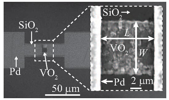
Figure 1.
(
a) The cross-section and (
b) top views of the wavelength-sized hybrid Si-VO
electro-absorption switch and photodetector presented in [
11]. (
c) A scanning electron micrograph of an etched VO
strip atop a Si rib waveguide. This would form the active region of an electro-absorption switch/modulator.
In this article, we present geometry-dependent scaling trends from current-voltage measurements of etched VO
microwires that are confirmed by thermal models and infrared optical imaging to study independently each step of the two-step phase transition in VO
. The optical and electrical properties of each transition can be used to design hybrid optoelectronic devices for switching, modulation and detection applications. In contrast to and complementing recent works to study the role of thermal effects in the electronically-induced phase transition in VO
[
32,
35] and radio frequency measurements of VO
strips integrated into coplanar waveguides [
36], this work primarily uses DC electrical measurements of etched VO
microwires with a range of geometries to infer different mechanisms for each step of the phase transition. The measurements show that the first step is a carrier-induced phase transition between the insulating (I) and an intermediary, partially-metallic phase (M
) that results in a delocalized change in the optical absorption and resistivity with almost no hysteresis; the second step is a thermally-induced phase transition to the metallic phase (M) that exhibits a wide hysteresis and is due to Joule heating as a result of current filamentation. The first transition has a smaller hysteresis and is expected to occur on a shorter time scale, which makes it suitable for optical modulation applications requiring high operation speeds and small hysteresis. Additionally, a small hysteresis allows the devices to operate with a smaller swing voltage, if they are biased close to the phase transition point. In contrast, the second transition is suitable for achieving the maximum extinction ratio.
Although the current-induced two-step phase transition in VO
has been previously observed [
35,
37], the nature of each transition was not clarified, and geometrical control over the transition thresholds was not established. Recent experiments have shown that charge injection can cause VO
to be in a partially-metallic phase without any structural change [
32] (or the “mixed-phase” in [
38]). We infer that the first transition observed here would correspond to this effect, while the change to the tetragonal crystalline structure in the metallic phase would occur in the second transition. The optical infrared imaging results presented here are also the first report of measured absorption changes after the first transition. Overall, this work helps to understand the causes of the phase transition in VO
and provides guidelines for the geometry of VO
devices to achieve efficient and/or high-speed optical and electronic switching.
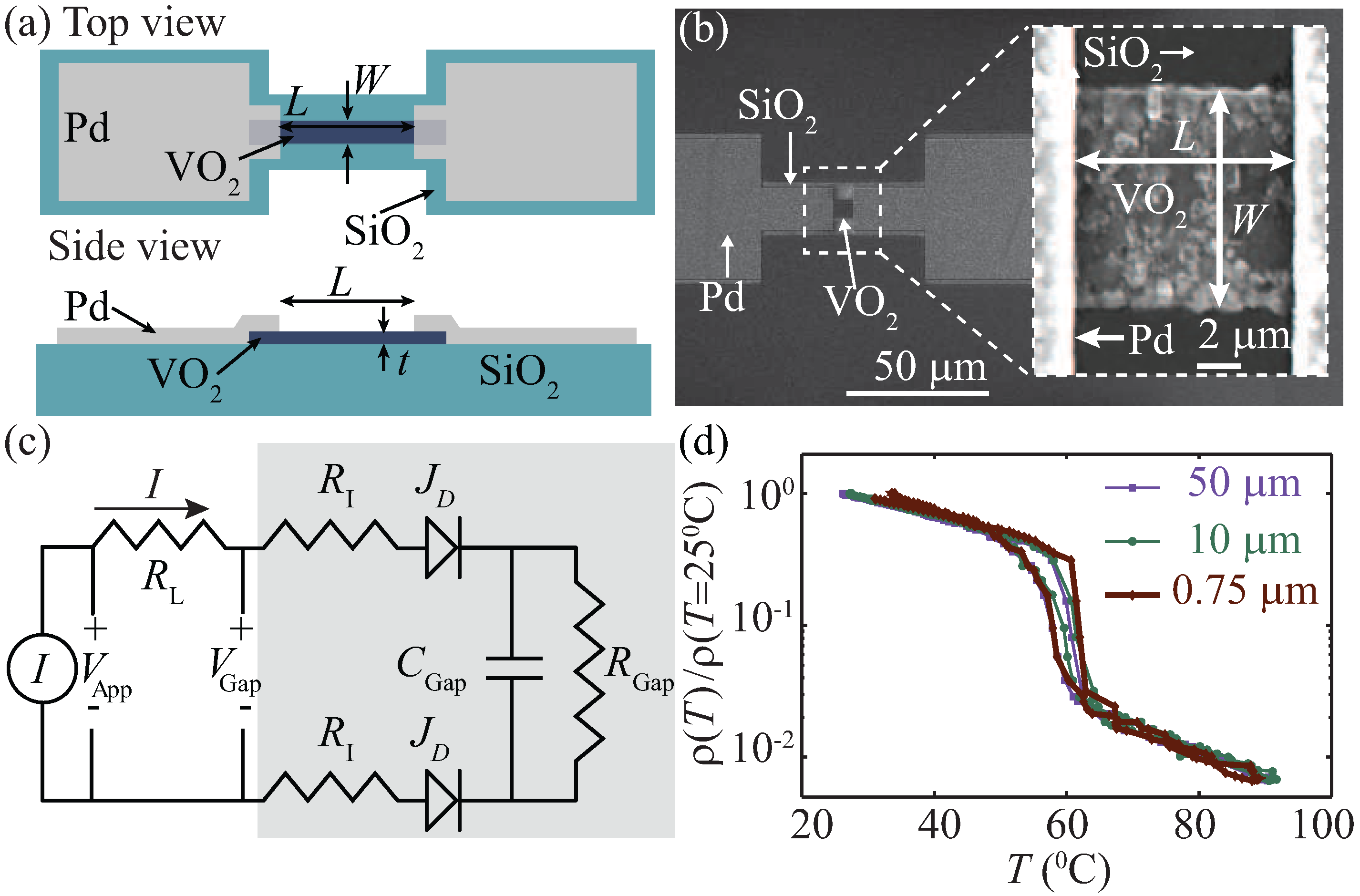
Figure 2.
(a) The top and side view schematics of a VO lateral junction. (b) A scanning electron micrograph of the device and (inset) the magnified image of the gap. (c) The equivalent circuit model of the device in the experiment. (d) The normalized resistivity of different microwires measured as the substrate temperature, T, for μm and 750 nm, 10 μm and 50 μm.
2. Fabrication and Device Geometry
VO
microwires, as illustrated in
Figure 2a, were fabricated using electron-beam (e-beam) lithography and reactive ion etching of a 100 nm-thick VO
film that was sputtered on a 2 μm-thick thermally-grown silica (SiO
) on a silicon (Si) substrate [
12]. The grain sizes of the samples, as measured using scanning electron microscopy, were about 75 ± 25 nm. Lateral electrical contacts were defined using aligned e-beam lithography followed by e-beam evaporation and lift-off of a 100 nm-thick palladium (Pd) film. The contacts were separated by a gap of length
L, which varied between 0.15 μm and 7.5 μm. The microwire width,
W, varied between 0.75 μm and 50 μm.
Figure 2b shows a scanning electron micrograph of a device with
μm and
μm. Details about the sample preparation and fabrication are described in
Appendix A.
A circuit model for the experiments is shown in
Figure 2c. A current,
I, was applied to the device under test using a precision sourcemeter, and the voltage across contacts,
, was measured. An external resistance of
kΩ limited the current. The VO
microwire was modelled as a resistance,
, in parallel with a capacitance,
[
33]. The interface between the VO
and a Pd contact was modelled as a contact and an interface sheet resistance,
, as well as a Schottky diode (due to the work function mismatch between Pd and VO
) with current density
[
39]. This simple circuit model is useful for predicting the total resistance of the etched VO
microwires as described in
Appendix B2. The model also shows that for the dimensions studied here, the VO
microwires had essentially the same material properties as the bulk film, which were not affected by the etching. This is further confirmed by the measurements of the resistivity,
, as a function of the substrate temperature. As an example,
Figure 2d shows the measured resistivities for microwires with
μm and
750 nm, 10 μm and 50 μm. The transition temperature and normalized resistivity were independent of
L and
W, indicating that devices of this size can be modelled by the bulk material properties of VO
.
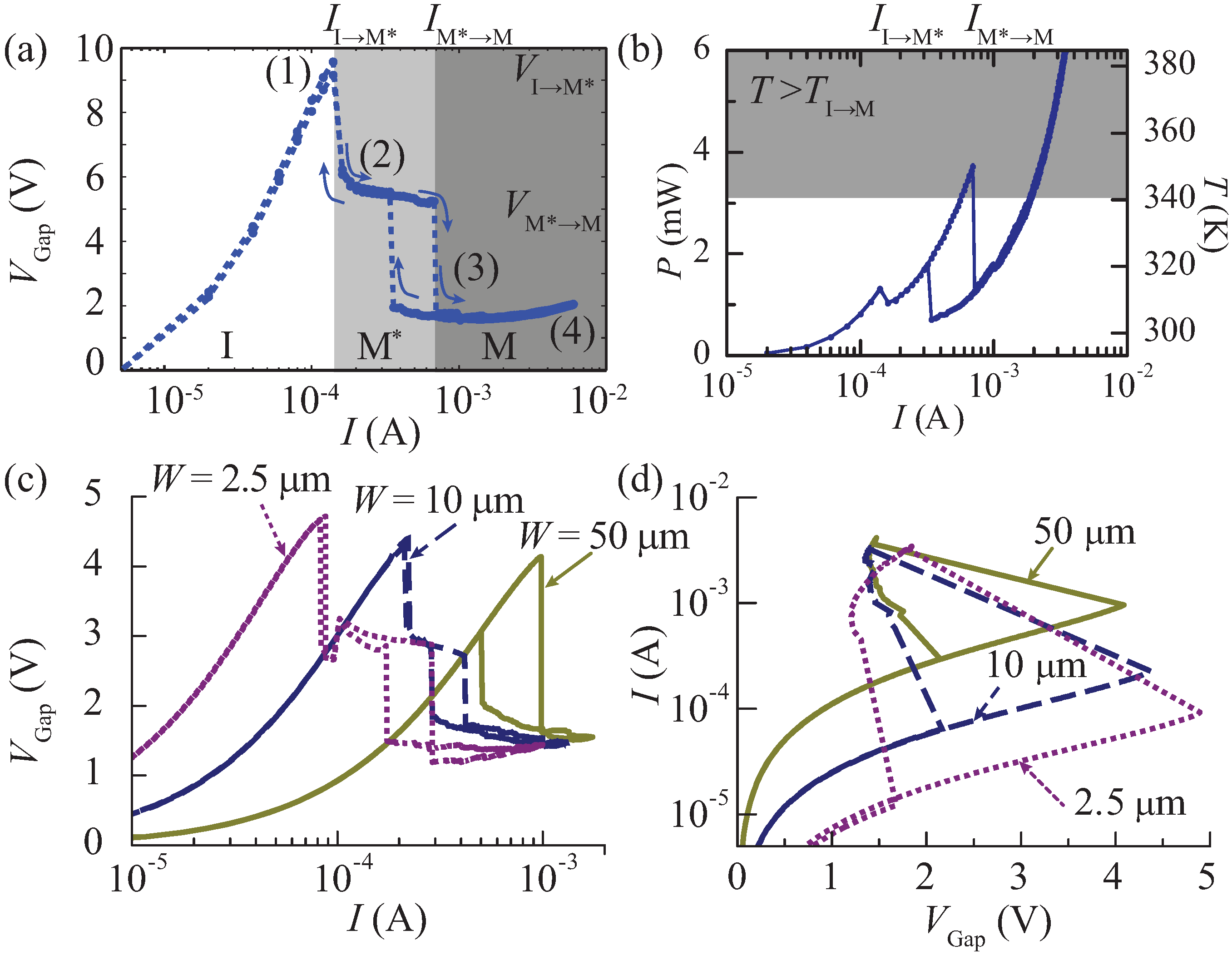
3. Current-Induced Phase Transition
By controlling the current applied to a microwire, a two-step phase transition could be clearly observed. As an example,
Figure 3a shows the measured
as a function of
I for the
μm and
μm device. The arrows in the figure trace
, and the shaded regions highlight the different VO
phases at each current range. The drop in
was a direct manifestation of the phase transition and occurred in two steps. The first transition from the insulating to a partially-metallic phase (I→M
) occurred at a current
and voltage
with a narrow hysteresis width. The second transition from the partially-metallic phase to the metallic phase (M
→M) occurred at a current
, voltage
and exhibited a wider hysteresis loop.
Figure 3.
The (a) voltage-current and (b) power-current relationship of a the VO wire with μm and μm. The expected temperature of the VO is included in the right axis. (c) The voltage-current and (d) current-voltage relationship of a the VO wire with μm and 2.5 μm, 10 μm and 50 μm.
Figure 3.
The (a) voltage-current and (b) power-current relationship of a the VO wire with μm and μm. The expected temperature of the VO is included in the right axis. (c) The voltage-current and (d) current-voltage relationship of a the VO wire with μm and 2.5 μm, 10 μm and 50 μm.
To determine the thermal contribution to each transition, we first simulated using a finite element method (COMSOL Multiphysics) the maximum temperature in the VO
during the two-step transition by taking the measured dissipated electrical power,
, as a Joule heat source (see
Appendix B1 for details).
Figure 3b shows
P (left axis) and the simulated temperature,
T, (right axis) of the VO
slab, as a function of
I.
T was less than
at the first transition and reached
just before the second transition. These results strongly suggest that the second transition is thermally induced and results in a fully-metallic phase, while the first transition is of a different physical origin due to the applied currents and results in a partially-metallic phase.
The current thresholds,
and
, strongly depended on the geometry of the wire. As an example,
Figure 3c shows the
V I characteristics of three different wires with
μm and different widths of
2.5 μm, 10 μm and 50 μm. As
W increased, both
and
increased, but at different rates, indicating that the two transitions were differently affected by the wire geometry. When
μm and
μm, the two transition thresholds almost overlapped and appeared almost as a single transition from the I to M phase. The two-step phase transition only occurred when the current was regulated.
Figure 3d shows the
characteristics of the devices of
Figure 3c, when a voltage source swept
. For all devices, only a single transition was observed. If the current was not controlled, a reduction in the resistance (e.g., caused by any carrier effects) would draw more current, thereby heating the device and initiating any thermally-driven step(s) in the phase transition. Therefore, to study the two-step phase transition, it is essential to regulate the current throughout the phase transition.
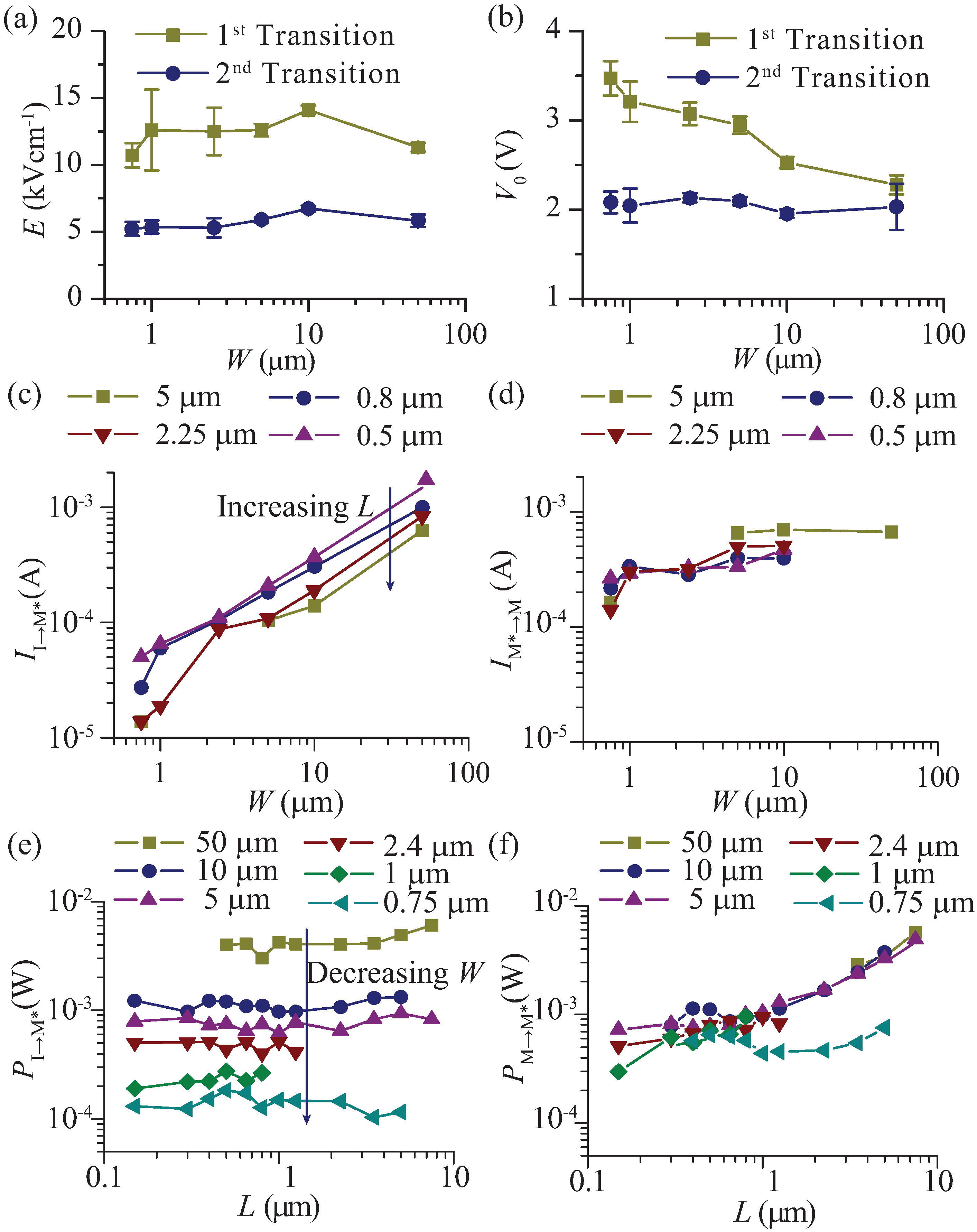
3.1. Critical Electric Fields
To investigate the origin of the each transition, we examined the electric field, current and power dissipation of devices with varying widths and lengths. From the measured
and
of microwires with different lengths, we determined the “average” electric fields in the gap for the first (
) and second (
) phase transitions from the slopes of the transition voltages
vs. length
L (at each width,
W).
Figure 3a shows that
and
were roughly constant and were approximately
kV/cm and
kV/cm, respectively. The field transition thresholds were independent of the wire geometry and were intrinsic properties of the VO
. Although
was roughly constant with
W,
varied significantly with
W (for the same
L) due to the VO
-Pd interface resistance. The effect of the interface is well modelled by the circuit in
Figure 2 and described in
Appendix B2. The interface resistance was a result of electron scattering and the work function mismatch. The interface resistance increased with decreasing
W and resulted in higher values of
.
From the
and
vs.
L relations, we extrapolated the offset voltages of the transition voltages,
i.e., the transition voltages as
, as shown in
Figure 4b.
decreased with increasing
W for the first transition, as expected from decreasing the interface resistance. The second transition had a lower
since the resistivity of the VO
had been reduced by about one order of magnitude after the first transition. Interestingly,
for the second transition was nearly independent of
W, suggesting that the second phase transition was spatially localized to a width less than
W. Filamentation is a signature of a thermally-induced transition in VO
[
40], which is accompanied by a structural phase transition [
29].
3.2. Threshold Current Densities
The different mechanisms behind the two phase transitions are further manifested in the device geometry dependence of the currents,
and
, and dissipated power,
and
, at the phase transitions.
Figure 4c,d shows that, unlike the transition electric fields,
and
exhibited scaling trends with
W.
increased almost linearly with
W, and we extrapolated a threshold current density for the first transition of
kA/cm
. This current density is related to the VO
carrier density,
n, through the drift current relation,
where
q is the elemental charge and
is the VO
electron mobility [
41], which is about
cm
V·s). The critical carrier density for the first transition was about
cm
. In contrast,
was nearly constant with
W, which again implies that the second transition was spatially localized. The different dependences of
and
on
W and
L further emphasize the geometrical control over the two-step transition. The separation between the two transitions decreases with increasing
W, and eventually, a single transition is observed when
.
Figure 4.
(a) The “average” electric field and (b) the transition voltage offset for both transitions vs. W. The transition currents for the (c) first and (d) second transitions as a function of W for several values of L. The dissipated power density for the (e) first and (f) second transitions as a function L for several values of W.
Figure 4e shows that
was essentially independent of
L and only varied by
over the two orders of magnitude of change in
L. This is further evidence that the first transition was not thermally induced, since longer microwires would require higher powers to reach
for a thermal transition. Indeed, the second transition,
, shown in
Figure 4f, scaled linearly with
L, a confirmation that the second transition was thermally induced. However,
had almost no dependence on
W when
μm, indicating that the localized filament was a few microns wide. The width of the filament is likely affected by the thermal conductivity of the substrate and the homogeneity of the VO
film. The distinct dependences of transition currents and dissipated electrical power on the microwire geometry,
L and
W, can be used to specify devices that isolate one phase transition from the other.
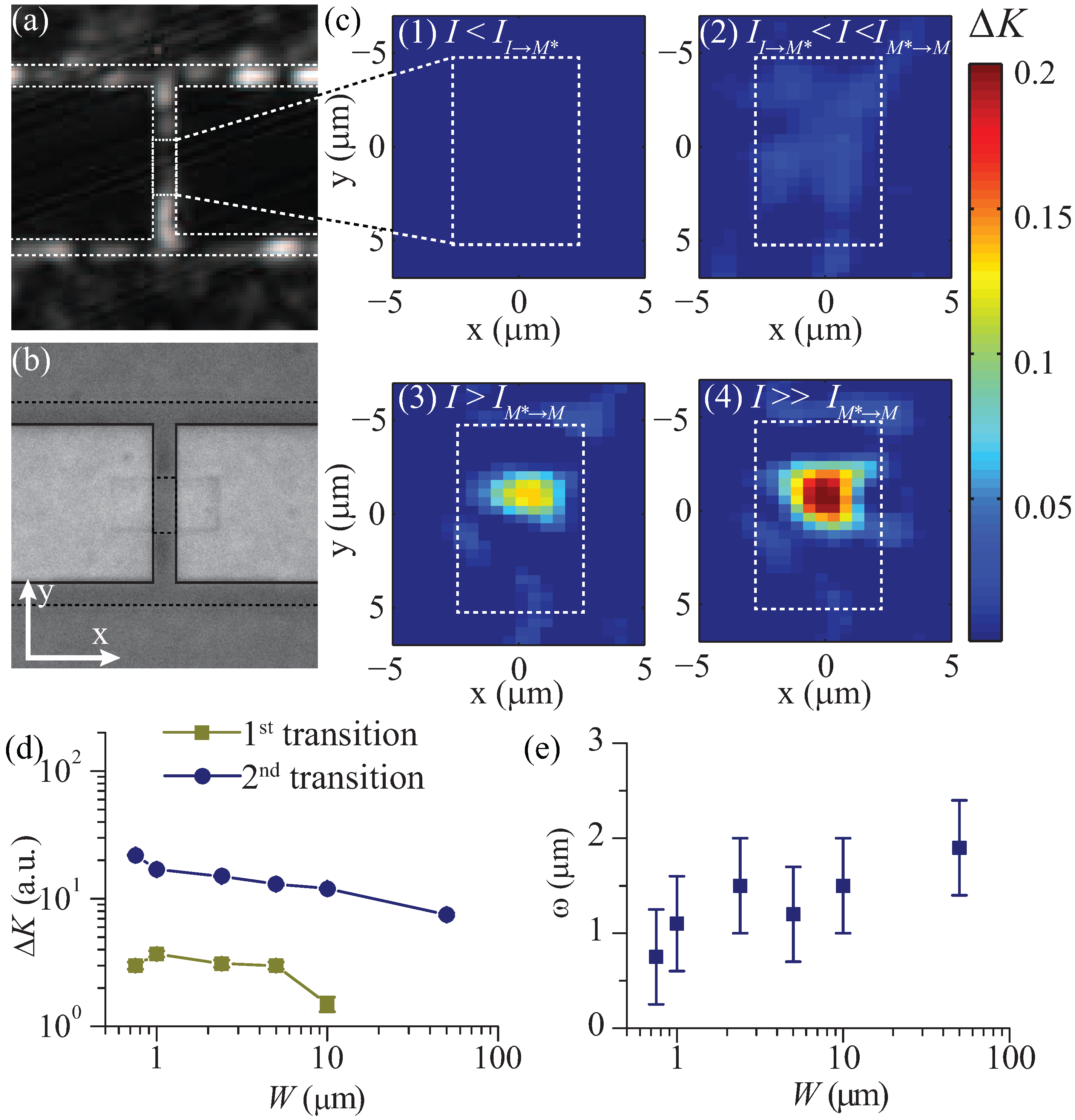
4. Optical Absorption
Finally, to directly visualize a delocalized electronic transition and filamentation in the thermal transition, we measured the spatial profile of the optical transmission,
K, of the VO
microwires using an erbium-doped fibre broadband light source with a centre wavelength of 1530 nm. Since this wavelength has an energy similar to the bandgap of VO
, it is sensitive to changes in the VO
near the bandgap. Previous visible light imaging experiments have reported no detectable change in the optical transmission during the first phase transition [
38].
Figure 5a,b, respectively, shows the infrared (IR) and visible images of the device with
μm and
μm.
Figure 5c shows the decrease in the transmission extracted from the IR images normalized to the transmission when no current is applied. The change in the transmission,
, is defined as:
The parenthesized numbers in
Figure 5c correspond to the currents labelled in
Figure 3a, and the boundaries of the VO
microwire are marked with white dashed lines.
Figure 5c-1 shows no detectable change in the transmission when
.
Figure 5c-2 shows that after the first transition, the VO
was in the M
phase, and
increased to
% over the entire microwire. After the second transition, as shown in
Figure 5c-3, the spatial profile of
collapsed to a filament and
increased to
%. At this point, the filament is composed of VO
in its M phase. Beyond
, as shown in
Figure 5c-4, the filament width and the spatial extent of the M phase grew and
increased to
%. The change in the optical transmission,
, for the two transitions as a function of
W for microwires with
μm is summarized in
Figure 5d.
for the first transition was at least 10× smaller than the second transition.
Figure 5e shows the imaged full-width at half-maximum (FWHM) of the filament,
ω, after the second transition for microwires with
μm. In agreement with the electric field, current and power dissipation measurements (
Figure 4b,d,f), the second phase transition was spatially confined to a filament that was 1 to 2 μm wide when
μm.
Figure 5.
The (
a) infrared and (
b) visible optical images of the VO
device with
μm and
μm. (
c) The decrease in the infrared optical transmission as the current is increased. Each sub-figure corresponds to a current labelled in
Figure 3a. (
d) The decrease in the infrared optical transmission after each transition and (
e) the width of the filament as a function of
W when
μm.
5. Discussion
The measurements presented here have shown that injected carriers can initiate two-step phase transition in VO microwires. The threshold current to initiate the first step of the phase transition is strongly dependent on the VO microwire length and width, while the second step is somewhat geometry independent down to widths of about 1 to 2 , because the phase transition is initially confined to a filament of this width. The two-step phase transition can appear as a single step in wide wires, when the threshold current required to reach the critical carrier density leads to heating beyond . The difference in the threshold currents between the two steps of the phase transition can be increased by decreasing the microwire width.
These results are important for device applications. For example, for switching or modulation devices requiring the largest change in the resistivity and optical absorption, the two steps of the phase transition should be used together, though the operation speed would be limited by the slow structural transition. In addition, the VO
region should be designed to be narrower than the filament (
μm in our films) for optimal efficiency. The initiation of both steps of the phase transition can be readily accomplished by sweeping the applied voltage rather than the current, since a controlled current can suppress the thermal effects that lead to the second step in the phase transition. As an example, the wavelength-sized hybrid Si-VO
electro-absorption waveguide optical switches implemented in [
11] used these principles. The length of the VO
region was kept to
μm to maximize the efficiency, and the device was driven by an applied voltage.
By controlling the current injection, it is possible to initiate the first electronic transition only without the second thermal step, which should lead to faster devices, lower power thresholds and drastic reductions in the hysteresis. Reducing the hysteresis would reduce the amplitude of the modulation current necessary to operate the device and to lower the dynamic switching power. Current-controlled, rather than voltage-controlled VO
switching also leads to longer device lifetimes [
37]. Moreover, since the electronic phase transition is geometry independent (the optical absorption across the entire microwire is modified), it is possible to use a wider microwire atop a waveguide to achieve the same extinction ratio as a device that uses both steps of the phase transition. However, narrower microwires have the advantage of having a larger threshold current difference between two steps of the phase transition.
