Mode Heterogeneous Multimode Power Splitter Based on Cascaded Mode-Dependent Splitters and Converters


1
State Key Laboratory of Integrated Optoelectronics, Institute of Semiconductors, Chinese Academy of Sciences, Beijing 100083, China
2
School of Electronic, Electrical and Communication Engineering, University of Chinese Academy of Sciences, Beijing 100049, China
3
College of Materials Science and Opto-Electronic Technology, University of Chinese Academy of Sciences, Beijing 100049, China
*
Author to whom correspondence should be addressed.
Photonics 2024, 11(5), 457; https://doi.org/10.3390/photonics11050457
Submission received: 23 April 2024
/
Revised: 10 May 2024
/
Accepted: 12 May 2024
/
Published: 14 May 2024
(This article belongs to the Special Issue Optical Communication, Sensing and Network)
Abstract
:To the best of our knowledge, a novel concept of mode heterogeneity for the design of multimode devices is presented in this paper and applied to the design of scalable multimode power splitters. Based on a cascade of mode-dependent splitters and converters, we achieve beam splitting and mode conversion for four modes from to in the bandwidth from 1525 nm to 1560 nm. The measurements of the device at 1550 nm show excellent performance, with the insertion loss ranging from 0.16 dB to 0.63 dB, crosstalk all below −16.71 dB, and power uniformity between 0.026 dB and 0.168 dB.
1. Introduction
Silicon-based optical interconnect technology [1,2,3] has experienced rapid development in response to the escalating demand for communication capacity, driven by its advantages of high integration, broad bandwidth, and compatibility with the complementary metal oxide semiconductor (CMOS). To alleviate this increasing capacity pressure, extensive research has been conducted on multiplexing techniques [4], aiming to expand the communication capacity by introducing new communication dimensions into the system. One promising approach is mode-division multiplexing (MDM) systems [5,6,7], which load signals onto mutually orthogonal modes, enabling capacity expansion within a single wavelength channel. The multimode power splitter, as the essential device for building mode-insensitive optical networks and systems, has received widespread attention and research in recent years.
The demonstrated multimode power splitters can be categorized into two types. The first type operates on all input modes within the same structure such as tapered directional couplers [8] and optimized adiabatic couplers [9] that utilize the same coupling strategy for multiple modes to achieve power splitting. The self-imaging principle of multimode interference couplers [10,11] is used to realize the splitting function for low-order modes. There are also reports on inverse designs [12,13] and geometric optics-based structures [14,15]. Most of these designs are only effective in low-order modes, exhibiting limited performance and causing a spike in device size when scaled up to higher-order modes.
Conversely, the second type of multimode power splitter employs the cascaded architectures for the sequential operation of various modes. These include the architectures that convert each mode to a higher-order mode and then couple it to the corresponding mode through Y-branching [16]. A more recent type of beam splitter architecture utilizes a particle swarm optimization (PSO) algorithm to optimize the tapered couplers, achieving a splitter with 3 dB splitting of modes under broadband [17]. This class of multimode power splitters possesses scalability but poor equalization of multiple modes at both outputs.
Modes serve as signal carriers in MDM systems due to the orthogonality of the same polarization modes, ensuring that distinct signals do not interfere with each other. Previous designs of multimode devices followed a one-to-one correspondence between the carrier mode of the input signal and the carrier mode of the output signal. An easily conceivable way to do this is to demultiplex the modes sequentially into the two sets of fundamental modes and then couple the fundamental modes back to their original modes in the output waveguides on two sides, respectively [17]. This introduces an additional multiplexing/demultiplexing stage in the MDM system, which would greatly increase the complexity of the system. This correspondence imposed limitations on device design, as it is unnecessary to strictly maintain the invariance of carrier modes throughout the entire signal transmission link. Instead, the primary requirement is to ensure the orthogonality of carrier modes to prevent interference between signals. We propose here the novel concept of mode heterogeneity. That is, in an MDM system, the multimode device does not need to maintain the correspondence between signals and modes but only the orthogonality of the modes in the whole link, and the composition of the modes of the signal group is allowed to be differently constituted.
In this paper, we propose a straightforward and scalable multimode 3 dB power splitter with cascaded mode-dependent splitters and converters based on the concept of mode heterogeneity. The multimode splitter supporting four modes () is demonstrated here, which can evenly separate four sets of signals within a single channel into two spatial channels in an MDM system. The device exhibits excellent performance from 1525 nm to 1560 nm, with the insertion loss below 1.14 dB for all four modes, crosstalk less than −14 dB, and power uniformity less than 0.46 dB for the first three modes and below 1.05 dB for the mode.
2. Design and Simulation
2.1. Principle
Figure 1a shows a schematic of the mode heterogeneous multimode power splitter (MH-MPS) in both 3D and cross-sectional views. The proposed device can be divided into four stages. Each section is a mode-dependent splitter and converter (MDSC) that allows the splitting and conversion of specific input modes to specific output modes. The MDSCs serving different input and output modes are sequentially connected by the taper. When a set of signals (A, B, C, and D) corresponding to the carrier modes (, , , and ) is input, the D signal is split in the first part and the signal carrier mode is converted to while other low-order modes will directly pass through. Additionally, the output is passed through to the other MDSC sections and can consequently be transmitted to the final port in the outermost two sets of waveguides. Figure 1a illustrates that the input signals (A, B, C, and D) are split into spatial channels on both sides, and the signal carrier modes are distributed heterogeneously without correspondence.
Each stage of the MDSCs, as illustrated in Figure 1a, is symmetrical and consists of seven parallel straight waveguides, sequentially numbered as waveguides 1 to 4. The gap between the waveguides is all 180 nm. Figure 1b shows the variation in the effective refractive index versus the waveguide width for the four modes. The widths of waveguides 4 and 1 on both sides of the MDSC should be chosen to match the corresponding input target mode and the output target mode, and the widths of waveguides 2 and 3 between them correspond to the fundamental mode. In this paper, we take the matched waveguide widths corresponding to the four modes to be 0.36 μm, 0.76 μm, 1.16 μm, and 1.56 μm. Such widths satisfy that the effective refractive index of the highest-order modes that each waveguide supports are matched. In this way, the target input and output modes are coupled within the MDSC and the coupling effect of the low-order modes is weak [18]. To suppress the crosstalk generated by the coupling between the tapers used to connect the MDSCs, it is necessary to maintain a sufficient distance between the waveguides 1 and 4 connected to the tapers, and that will make the distance between the tapers sufficiently large. Additionally, to maintain the coupling of the target modes, waveguides 2 and 3 should be introduced between waveguides 1 and 4. The eigenmodes within the MDSC, which can be calculated with an EME solver (Ansys Lumerical), are a series of supermodes with different distributions.
Taking the second stage as an example, the input modes are all the output modes of the first stage, which are in the two waveguides 1 and , , and in waveguide 4. Theoretically, these modes, when coupled into the MDSC, can be expressed as the sum of its eigenmodes. Figure 2 illustrates the distribution of the excited supermodes within the second MDSC when the modes are fed at different waveguide inputs. It is discussed here in two cases.
In the case where the input mode is the target mode , a series of supermodes are excited as shown in Figure 2a. Subsequently, because the propagation constants of the supermodes are different, the phase difference accumulated by each supermode will differ after a certain propagation distance. Ideally, the phase differences satisfy the condition, as shown in Figure 2a, so that the phase change of supermodes 1 and 2 is and that of supermodes 3 and 4 is , where n is a positive integer. The supermodes are linearly superimposed, resulting in two s being output at the end of waveguide 1.
The case of non-target mode inputs is illustrated in Figure 2b,c. When and are input from waveguide 4 and is input from waveguide 1, only one eigenmode can be excited, and the mode field distribution is almost the same as that of the input modes. The distribution of supermodes is confined within waveguides 1 and 4, as shown in Figure 2b,c. For target modes, the device has beam splitting and mode switching capabilities while maintaining the straight-through capability for non-target modes. This characteristic ensures the sequential conversion and beam splitting of the four modes input from waveguide 4 into waveguide 1 on both sides. Simultaneously, the target output mode converted by the MDSC will not be coupled in the next stage, resulting in four heterogeneous modes at the outputs on both ports.
2.2. Optimization
However, the phase shift of the individual supermodes may not exactly satisfy the ideal relationship with , resulting in the superposition field of the supermodes still being partially distributed in waveguides 2, 3, or 4 after a certain transmission distance within the seven-waveguide structure. So, here we introduce a secondary multi-waveguide structure (SMWS) to improve the transmission efficiency. As shown in Figure 2a, an SMWS is connected to the end of the seven-waveguide structure so that a small portion of the optical energy distributed in waveguide 2 can be further coupled to waveguide 1 on both sides by the SMWS to achieve a more efficient conversion.
Considering that there can be many designs of SMWSs with different impacts on efficiency, we will only explore five optimized structures here for structural simplicity. Four of these SMWSs are constructed and their lengths are defined as the matching length (ML), as illustrated in the optimized schematic in Figure 3a. For a given ML, the optimum efficiency is obtained by scanning the entire length of the structure. On this basis, the variation curve of the transmission efficiency can be obtained by changing the ML, as shown in Figure 3b–d. Based on the results, stage 1 was selected to be optimized as structure 1, and stages 2 and 3 were optimized as structure 4. However, the phase difference of the supermodes within the fourth stage is so large from the ideal case that it is difficult to achieve efficient transmission efficiency with the above four structures. Here, we introduce two segments of the SMWS as shown in Figure 3e. By scanning the two MLs, the transmission efficiency of the fourth stage is obtained as shown in Figure 3f.
With both and at 0.36 m, the overall design parameters of each stage are listed in Table 1. Multiple MDSCs are connected sequentially with tapers of a length Lt of 6 m. Because the sums of the widths and in all four stages are equal, the distance D between waveguide 1 and waveguide 4 on both sides of the power splitter remains constant at 1.26 m. This design avoids introducing crosstalk generated by the bending of the waveguides on both sides. To validate the above analysis, we calculated the optical propagation profile, as illustrated in Figure 4. Across the entire C-band, the insertion loss (IL) of the four modes () is less than 0.81 dB, 0.76 dB, 0.79 dB, and 0.77 dB in order, and their crosstalk is less than −31.8 dB, −22.2 dB, −21.7 dB, and −26.7 dB in order. At 1550 nm, the insertion loss ranges from 0.15 dB to 0.3 dB for all modes, with the mode crosstalk varying between −22.17 dB and −33.5 dB. Obviously, the insertion loss of the four modes shows a gradual increase when the wavelength is far from the center wavelength. This is because the effective refractive indices of the supermodes within the multi-waveguide structure are not the same at different wavelengths, causing the coupling efficiency at a fixed length to vary with wavelength.
At the same time, we simulated the fabrication errors. The results in Figure 5a show that the insertion loss of all four modes increases when the device size is reduced by 10 nm. Increasing the size by 10 nm also decreases the transmission efficiency, especially for the fundamental mode, as demonstrated in Figure 5b. Both of the above have a smaller increase in crosstalk. In general, the device is relatively sensitive to fabrication errors. The insertion loss and mode crosstalk at temperatures of 300 K and 350 K are shown in Figure 5c,d. It can be seen that the center wavelength of the insertion loss generally shifts toward the shortwave when the temperature is increased by 50 K. The comparison does not appear to show a large difference, proving that the temperature has a small effect on device performance. The functionality of the mode-heterodyne beam splitting has been effectively implemented.
3. Fabrication and Characterization
The designed MH-MPS was fabricated on an SOI platform at Advanced Micro Foundry, Singapore, with a top silicon layer of 220 nm and a buried oxide layer of 3 µm. Figure 6 shows the fabricated MH-MPS and the multimode bend used for normalization. In the lower part of the figure, light enters the mode multiplexer, passes through the MH-MPS and multimode S-bending, and exits the mode demultiplexer. When the amplified spontaneous emission is coupled to one of the inputs, the optical power of the eight output ports is measured sequentially with an optical spectrum analyzer. Then, the same operation is performed by switching to the other input. The transmission spectra of the device in the multi-group input mode are finally obtained. However, the measured results include the loss of the mode multiplexer/demultiplexer and the multimode bending; it is necessary to subtract the insertion loss of these two in the normalization. First, two sets of reference transmission spectra are measured, one including the S-bend and one including only the straight waveguide, followed by the transmission spectra including the MH-MPS. Considering the inconsistency between the target modes for the input and output within the device, the normalized spectrum requires subtracting the insertion losses of the mode multiplexer for the input mode and the S-bend and the mode demultiplexer for the output mode from the measured spectrum. The crosstalk (CT) and power uniformity (PU) of the MH-MPS are defined by the following equations:
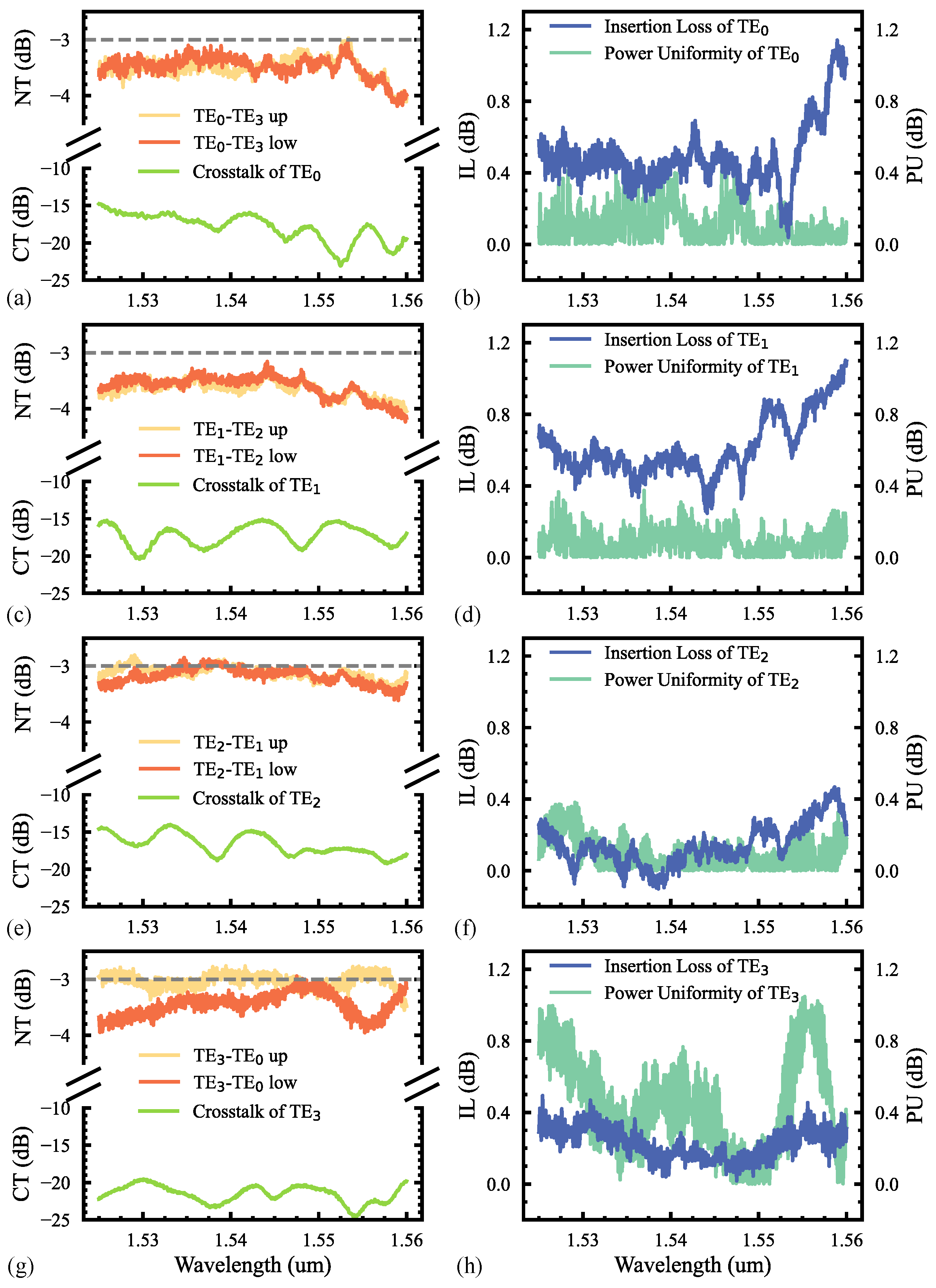
where n or m represents the order of the mode. () represents the optical power measured at the upper (lower) port when is the input mode and is the output mode. The insertion loss and the corresponding crosstalk and power uniformity in the wavelength range from 1525 nm to 1560 nm for each input mode that has been normalized are shown in Figure 7. The measured data are detailed in Table 2. There is some degradation in the measured data compared to the simulated data because the fabricated waveguide deviates from theory and the gaps are not uniform. Moreover, the device’s measurable bandwidth is constrained due to the limitations of the light source. The measured data show that the device meets the design requirements well at 1550 nm. In addition, lower losses and a wider operating bandwidth can be achieved by using coupling structures, such as tapered waveguides or subwavelength gratings. The design can be easily extended to operate more modes by simply varying the widths of the waveguides in the MDSC so that the widths of the middle waveguide 4 and waveguide 1 on both sides satisfy the matching conditions for the input or output target modes, followed by the optimization of the secondary multi-waveguide structure.
Additionally, some typical structures of multimode power splitters and our proposed MH-MPS are summarized in Table 3 while the performance and parameters of each structure are also given. As can be seen in Table 3, the device structures with better performance (the first four groups) can only be applied to low-order modes and are hardly scalable for higher-order modes. Meanwhile, although the application of subwavelength gratings or the inverse design approach brings more compact device structures, the corresponding minimum feature size is also required to be quite small. Correspondingly, the last three groups of device structures (including this work) have design principles that can be extended to meet the inputs of higher-order modes. While the structure proposed in Ref. [17] has a superior bandwidth, the main design principle is based on the multiplexing/demultiplexing of modes and optimization of the coupled waveguide using a particle swarm algorithm. This can make the whole design process extremely time consuming and cumbersome. In comparison, our proposed MH-MPS has scalability and excellent performance in a more compact device size. It is worth mentioning that, due to the high symmetry of the device structure, the power uniformity of the first three modes, as shown in Table 2, is lower than 0.46 dB. Only when the mode is input does the PU increases more dramatically, as demonstrated in Figure 7h.
4. Conclusions
In summary, we innovatively propose the design concept of mode heterogeneity, which eliminates the design limitations of conventional multimode devices that strictly satisfy mode correspondences. On this basis, we have designed and demonstrated a multimode power splitter with an operating bandwidth from 1525 nm to 1560 nm based on mode-dependent splitters and converters. The beam splitting function of four modes from to has been realized, and the insertion loss of all the modes varies from 0.16 dB to 0.63 dB at 1550 nm, the crosstalk is less than −16.71 dB, and the power uniformity is below 0.168 dB. The design principle of the device can be easily extended to higher-order modes. We believe it has great potential for application in large-scale integrated optical communication and MDM systems. Meanwhile, the concept of mode heterogeneity also provides a new way to design various devices in MDM systems.
Author Contributions
Conceptualization, X.X.; methodology, X.X. and H.C.; software, X.X.; validation, X.X.; formal analysis, X.X.; investigation, X.X.; resources, X.X.; data curation, X.X.; writing—original draft preparation, X.X.; writing—review and editing, X.X., H.C., and X.F.; visualization, X.X.; supervision, L.Y.; project administration, X.F. and L.Y.; funding acquisition, X.F. and L.Y. All authors have read and agreed to the published version of this manuscript.
Funding
This research was funded by The Strategic Priority Research Program of Chinese Academy of Sciences under Grant XDB43000000.
Institutional Review Board Statement
Not applicable.
Informed Consent Statement
Not applicable.
Data Availability Statement
Relevant data are available from the authors upon reasonable request.
Conflicts of Interest
The authors declare no conflicts of interest.
References
- Atabaki, A.H.; Moazeni, S.; Pavanello, F.; Gevorgyan, H.; Notaros, J.; Alloatti, L.; Wade, M.T.; Sun, C.; Kruger, S.A.; Meng, H.; et al. Integrating Photonics with Silicon Nanoelectronics for the next Generation of Systems on a Chip. Nature 2018, 556, 349–354. [Google Scholar] [CrossRef] [PubMed]
- Rahim, A.; Spuesens, T.; Baets, R.; Bogaerts, W. Open-Access Silicon Photonics: Current Status and Emerging Initiatives. Proc. IEEE 2018, 106, 2313–2330. [Google Scholar] [CrossRef]
- Chen, X.; Milosevic, M.M.; Stanković, S.; Reynolds, S.; Bucio, T.D.; Li, K.; Thomson, D.J.; Gardes, F.; Reed, G.T. The Emergence of Silicon Photonics as a Flexible Technology Platform. Proc. IEEE 2018, 106, 2101–2116. [Google Scholar] [CrossRef]
- Dai, D.; Bowers, J.E. Silicon-Based on-Chip Multiplexing Technologies and Devices for Peta-Bit Optical Interconnects. Nanophotonics 2014, 3, 283–311. [Google Scholar] [CrossRef]
- Li, C.; Liu, D.; Dai, D. Multimode Silicon Photonics. Nanophotonics 2019, 8, 227–247. [Google Scholar] [CrossRef]
- Luo, L.W.; Ophir, N.; Chen, C.P.; Gabrielli, L.H.; Poitras, C.B.; Bergmen, K.; Lipson, M. WDM-Compatible Mode-Division Multiplexing on a Silicon Chip. Nat. Commun. 2014, 5, 3069. [Google Scholar] [CrossRef] [PubMed]
- Wang, J.; He, S.; Dai, D. On-Chip Silicon 8-Channel Hybrid (de)Multiplexer Enabling Simultaneous Mode- and Polarization-Division-Multiplexing. Laser Photonics Rev. 2014, 8, L18–L22. [Google Scholar] [CrossRef]
- Luo, Y.; Yu, Y.; Ye, M.; Sun, C.; Zhang, X. Integrated Dual-Mode 3 dB Power Coupler Based on Tapered Directional Coupler. Sci. Rep. 2016, 6, 23516. [Google Scholar] [CrossRef] [PubMed]
- Han, L.; Kuo, B.P.P.; Alic, N.; Radic, S. Ultra-Broadband Multimode 3dB Optical Power Splitter Using an Adiabatic Coupler and a Y-Branch. Opt. Express 2018, 26, 14800–14809. [Google Scholar] [CrossRef] [PubMed]
- Liu, R.; Lu, L.; Zhang, P.; Chang, W.; Liu, D.; Zhang, M. Integrated Dual-Mode 3-dB Power Splitter Based on Multimode Interference Coupler. IEEE Photonics Technol. Lett. 2020, 32, 883–886. [Google Scholar] [CrossRef]
- Shiran, H.; Zhang, G.; Liboiron-Ladouceur, O. Dual-Mode Broadband Compact 2 × 2 Optical Power Splitter Using Sub-Wavelength Metamaterial Structures. Opt. Express 2021, 29, 23864–23876. [Google Scholar] [CrossRef] [PubMed]
- Chang, W.; Ren, X.; Ao, Y.; Lu, L.; Cheng, M.; Deng, L.; Liu, D.; Zhang, M. Inverse Design and Demonstration of an Ultracompact Broadband Dual-Mode 3 dB Power Splitter. Opt. Express 2018, 26, 24135–24144. [Google Scholar] [CrossRef] [PubMed]
- Xie, H.; Liu, Y.; Wang, Y.; Wang, Y.; Yao, Y.; Song, Q.; Du, J.; He, Z.; Xu, K. An Ultra-Compact 3-dB Power Splitter for Three Modes Based on Pixelated Meta-Structure. IEEE Photonics Technol. Lett. 2020, 32, 341–344. [Google Scholar] [CrossRef]
- Xu, H.; Dai, D.; Shi, Y. Ultra-Broadband on-Chip Multimode Power Splitter with an Arbitrary Splitting Ratio. OSA Contin. 2020, 3, 1212–1221. [Google Scholar] [CrossRef]
- Sun, C.; Ding, Y.; Li, Z.; Qi, W.; Yu, Y.; Zhang, X. Key Multimode Silicon Photonic Devices Inspired by Geometrical Optics. ACS Photonics 2020, 7, 2037–2045. [Google Scholar] [CrossRef]
- Xu, H.; Shi, Y. Ultra-Broadband Dual-Mode 3 dB Power Splitter Based on a Y-Junction Assisted with Mode Converters. Opt. Lett. 2016, 41, 5047–5050. [Google Scholar] [CrossRef]
- Chen, W.; Lin, J.; Li, H.; Wang, P.; Dai, S.; Liu, Y.; Yao, R.; Li, J.; Fu, Q.; Dai, T.; et al. Broadband Multimode 3 dB Optical Power Splitter Using Tapered Couplers. Opt. Express 2022, 30, 46236–46247. [Google Scholar] [CrossRef] [PubMed]
- Cooper, M.L.; Mookherjea, S. Numerically-Assisted Coupled-Mode Theory for Silicon Waveguide Couplers and Arrayed Waveguides. Opt. Express 2009, 17, 1583–1599. [Google Scholar] [CrossRef] [PubMed]
Figure 1.
(a) Three-dimensional schematic of the mode heterogeneous multimode power splitter and cross-sectional view of each stage. (b) Width dispersion curves for ,,, and .
Figure 1.
(a) Three-dimensional schematic of the mode heterogeneous multimode power splitter and cross-sectional view of each stage. (b) Width dispersion curves for ,,, and .

Figure 2.
The Ey distribution of the supermodes within the MDSC at stage 2, when target mode is input from waveguide 4 (a) and non-target modes are input from waveguide 4 (b) and waveguide 1 (c).
Figure 2.
The Ey distribution of the supermodes within the MDSC at stage 2, when target mode is input from waveguide 4 (a) and non-target modes are input from waveguide 4 (b) and waveguide 1 (c).
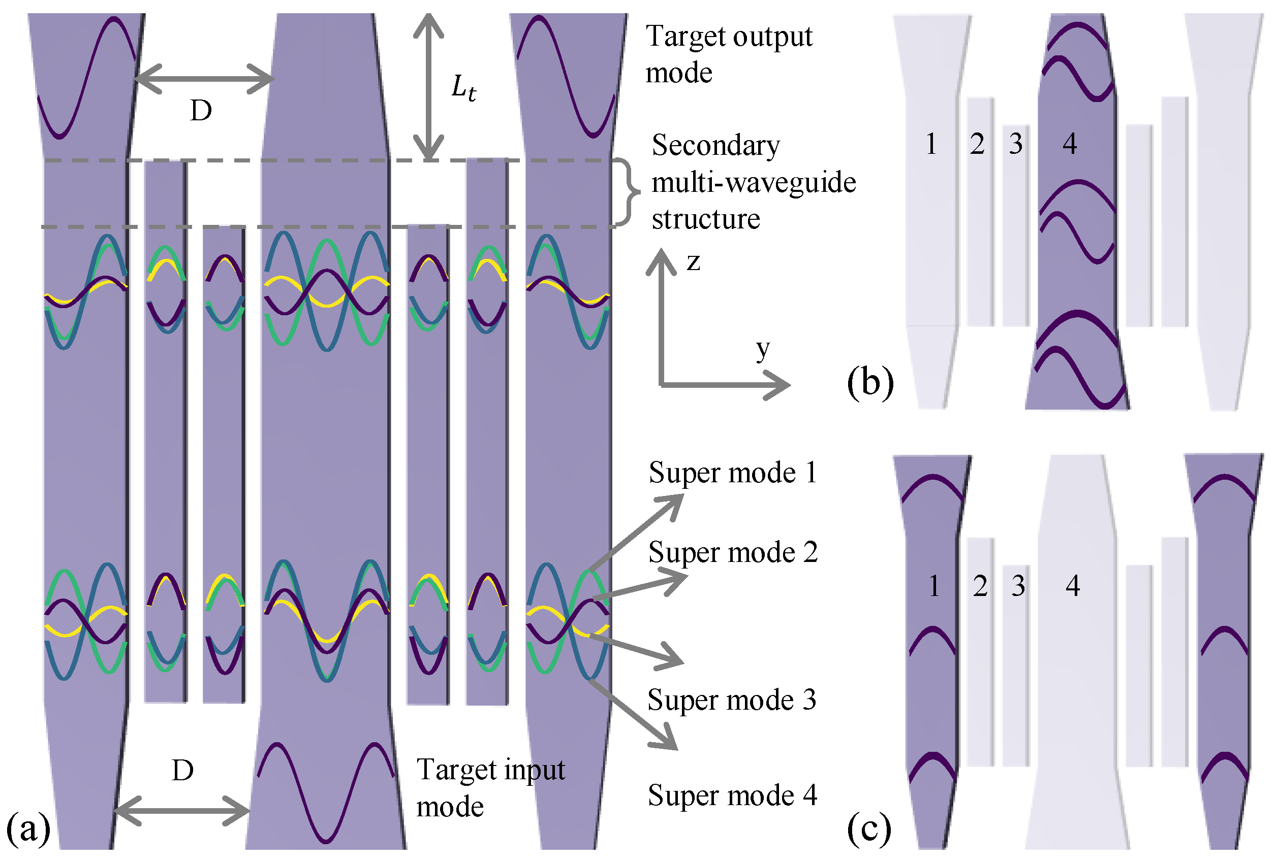
Figure 3.
The schematic structure for MDSC optimization in the first three (a) and the fourth (e) stages. (b–d,f) The transmission efficiency with the matching length for different optimized structures at 1550 nm.
Figure 3.
The schematic structure for MDSC optimization in the first three (a) and the fourth (e) stages. (b–d,f) The transmission efficiency with the matching length for different optimized structures at 1550 nm.
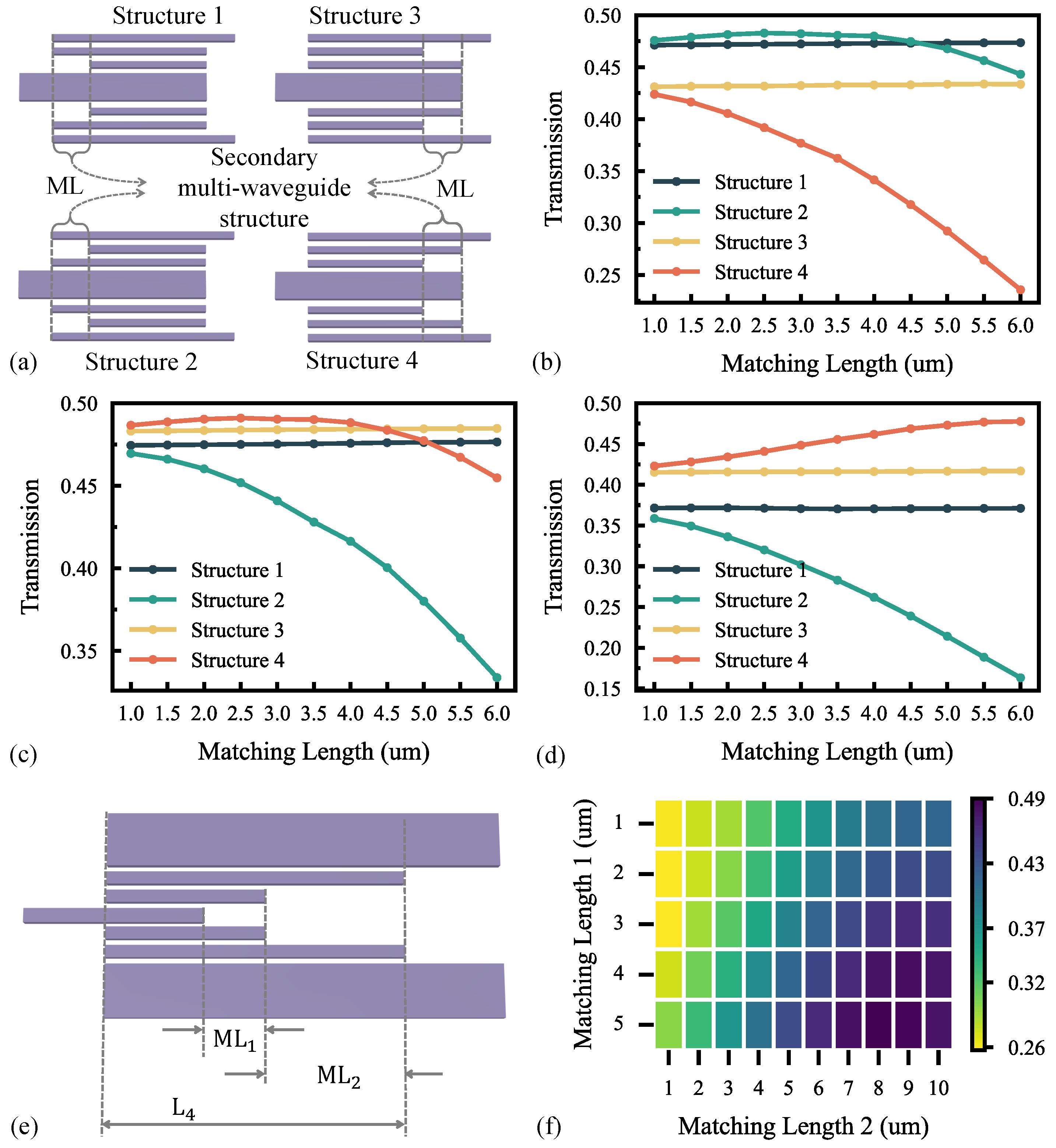
Figure 4.
The simulated insertion loss and crosstalk with the wavelength and light propagation at 1550 nm in the MH-MPS when the inputs are the (a), (b), (c), and (d) modes.
Figure 4.
The simulated insertion loss and crosstalk with the wavelength and light propagation at 1550 nm in the MH-MPS when the inputs are the (a), (b), (c), and (d) modes.
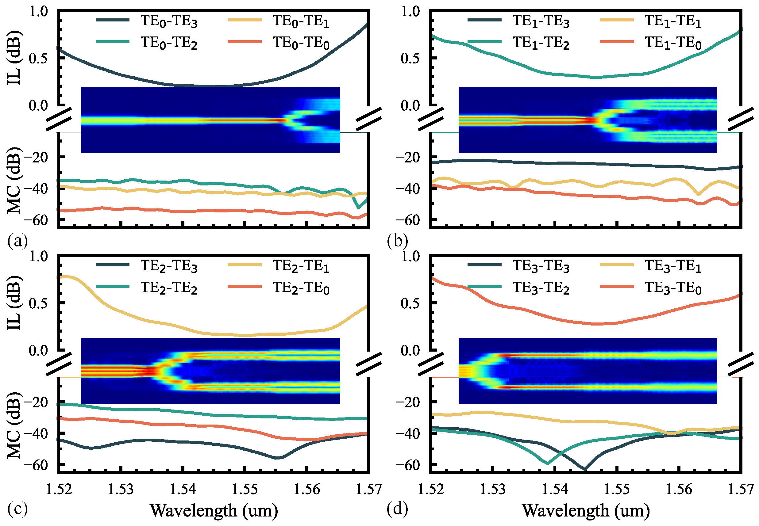
Figure 5.
Simulated insertion loss and crosstalk on fabrication error of −10 nm (a) and 10 nm (b) and at temperatures of 300 K (c) and 350 K (d).
Figure 5.
Simulated insertion loss and crosstalk on fabrication error of −10 nm (a) and 10 nm (b) and at temperatures of 300 K (c) and 350 K (d).
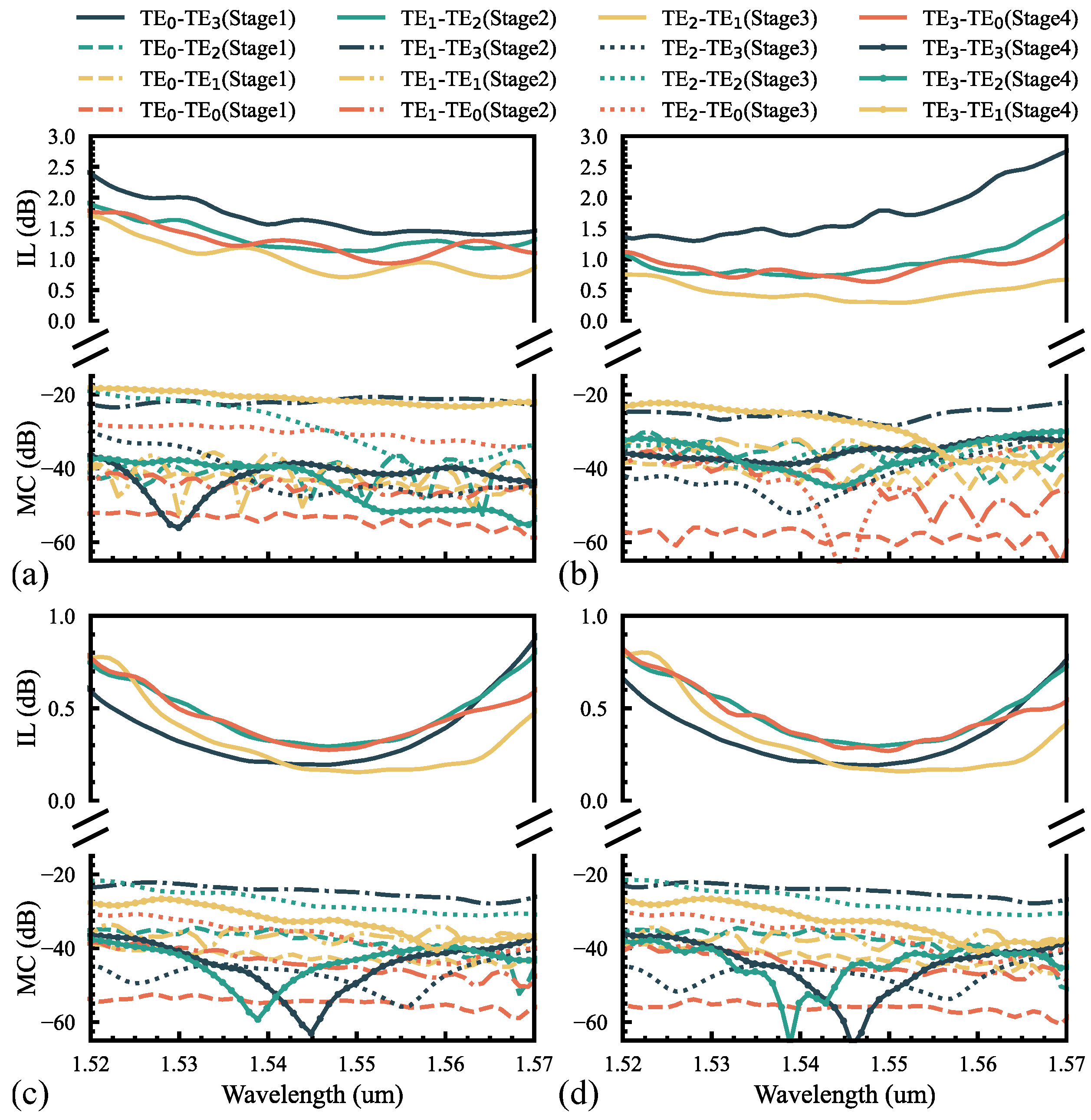
Figure 6.
Microscope image of the fabricated device and multimode bending used for normalization.
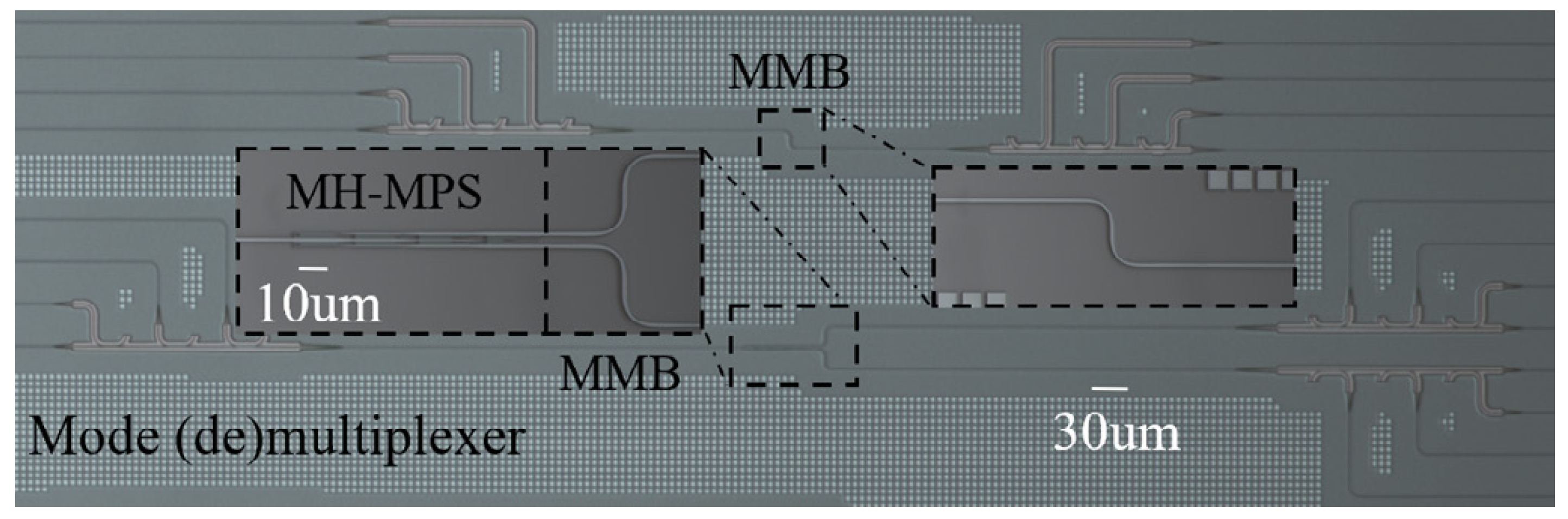
Figure 7.
The normalized transmission (NT) of the upper and lower ports, crosstalk (CT), insertion loss (IL), and power uniformity (PU) with the wavelength when the input modes are (a,b), (c,d), (e,f), and (g,h).
Figure 7.
The normalized transmission (NT) of the upper and lower ports, crosstalk (CT), insertion loss (IL), and power uniformity (PU) with the wavelength when the input modes are (a,b), (c,d), (e,f), and (g,h).

Table 1.
Design parameters of the MDSC at each stage, with two ML segments at stage 4.
| Stage | (μm) | (μm) | L (μm) | ML (μm) |
|---|---|---|---|---|
| 1 | 0.36 | 1.56 | 15.57 | 2 |
| 2 | 0.76 | 1.16 | 16.57 | 2 |
| 3 | 1.16 | 0.76 | 17.88 | 6 |
| 4 | 1.56 | 0.36 | 19.33 | 4; 9 |
Table 2.
Insertion loss, crosstalk, and power uniformity for modes.
| Input Mode | 1.525–1.56 μm | 1.55 μm | ||||
|---|---|---|---|---|---|---|
| IL (dB) | CT (dB) | PU (dB) | IL (dB) | CT (dB) | PU (dB) | |
| <1.14 | <−14.8 | <0.46 | 0.47 | −18.79 | 0.026 | |
| <1.1 | <−15.08 | <0.38 | 0.63 | −16.7 | 0.032 | |
| <0.47 | <−14 | <0.38 | 0.26 | −17.64 | 0.074 | |
| <0.49 | <−19.53 | <1.05 | 0.16 | −19.53 | 0.168 | |
Table 3.
Performance comparison of proposed MH-MPS with other reported multimode power splitters.
| Structure | Modes | Length (μm) | BW (nm) | IL (dB) | CT (dB) | PU (dB) |
|---|---|---|---|---|---|---|
| MMI [10] | 96.9 | 1530–1590 | <0.76 | <−20.50 | <0.9 | |
| SWG MMI [11] | 48.84 | 1500–1600 | <0.65 | <−17.00 | - | |
| Inverse design [12] | 2.88 | 1520–1580 | <1.50 | <−20.00 | - | |
| Inverse design [13] | 4.5 | 1530–1570 | <1.50 | <−15.00 | <0.35 | |
| Y-junction assisted with mode converters [16] | 120 | 1530–1610 | < 2.65 | <−13.30 | - | |
| Splitter using tapered couplers (PSO) [17] | 120 | 1520–1600 | <1.50 | <−14.12 | <0.88 | |
| This work | 87 | 1525–1560 | <1.14 | <−14.00 | <1.05 |
Disclaimer/Publisher’s Note: The statements, opinions and data contained in all publications are solely those of the individual author(s) and contributor(s) and not of MDPI and/or the editor(s). MDPI and/or the editor(s) disclaim responsibility for any injury to people or property resulting from any ideas, methods, instructions or products referred to in the content. |
© 2024 by the authors. Licensee MDPI, Basel, Switzerland. This article is an open access article distributed under the terms and conditions of the Creative Commons Attribution (CC BY) license (https://creativecommons.org/licenses/by/4.0/).
Share and Cite
MDPI and ACS Style
Xu, X.; Chen, H.; Fu, X.; Yang, L. Mode Heterogeneous Multimode Power Splitter Based on Cascaded Mode-Dependent Splitters and Converters. Photonics 2024, 11, 457. https://doi.org/10.3390/photonics11050457
AMA Style
Xu X, Chen H, Fu X, Yang L. Mode Heterogeneous Multimode Power Splitter Based on Cascaded Mode-Dependent Splitters and Converters. Photonics. 2024; 11(5):457. https://doi.org/10.3390/photonics11050457
Chicago/Turabian StyleXu, Xin, Hongliang Chen, Xin Fu, and Lin Yang. 2024. "Mode Heterogeneous Multimode Power Splitter Based on Cascaded Mode-Dependent Splitters and Converters" Photonics 11, no. 5: 457. https://doi.org/10.3390/photonics11050457
Note that from the first issue of 2016, this journal uses article numbers instead of page numbers. See further details here.