1. Introduction
Sic materials find wide-ranging applications in advanced optical systems within the aerospace, space exploration, astronomical observation, and high-intensity laser fields [
1]. However, as a ceramic material, Sic has certain drawbacks. Firstly, its surface lacks density, leading to a post-polishing roughness that fails to meet high-precision requirements [
2]. Secondly, Sic has the characteristics of high hardness, so it is difficult to directly process Sic to obtain high-quality optical mirrors. In order to deal with these problems, the Sic substrate is usually processed to a certain precision, the PV value of the surface shape accuracy of the substrate surface should be controlled at 1λ (λ = 632.8 nm), the surface roughness of the substrate Ra < 5 nm, and then a dense silicon modified layer is plated on the surface [
2,
3,
4]. This approach leverages the dual advantages of the Sic substrate and the modified silicon layer, ultimately enhancing the overall performance [
5]. Finally, the further processing of the modified silicon layer allows for the production of high-precision reflective mirrors [
6,
7,
8,
9].
The high hardness, significant brittleness, and low fracture toughness of materials like Sic present challenges in achieving high-quality optical surfaces due to the presence of cracks and microcracks. Therefore, ensuring the plastic removal of hard and brittle materials during the polishing process is crucial. Previous studies, both domestic and international, have conducted nanoindentation and nanoscratching experiments on typical hard and brittle materials like silicon, glass, and ceramics, demonstrating the existence of plastic removal depths. Mengran Ge et al. [
10] conducted machining experiments on single-crystal silicon (100) surfaces using nanoindentation and Berkovich diamond tips along the [010] crystal orientation. During the scratching process, the tangential friction force transitioned from stable to oscillatory as the normal force varied between 0 and 50 mN, and the material removal mode changed from plastic to brittle. The critical normal force for the plastic-to-brittle transition was determined to be 26 mN, resulting in a scratch depth of 353 nm. Yang Xiao et al. [
11] utilized blunt spherical tips and the elastic–plastic contact formula for brittle materials to explain the contact between the micro-cutting edges and brittle materials. Combining the critical load equation for indentation, they established a computational model for predicting the critical cutting depth, determining this for KDP crystal material to be 230 nm. Bifano et al. [
12] employed a micro-indentation method to establish the critical cutting depth for hard and brittle materials. When materials were removed plastically, and the surface cracks in hard and brittle materials were less than 10%, the critical depth of indentation (dc) was estimated. Ling Yin et al. [
13] used nanoindentation to study the plastic-to-brittle deformation of 6H-SiC (0001) substrate surfaces. The results showed that during indentation, there was a scale effect in the deformation of the 6H-SiC (0001) substrate, with plastic deformation occurring at nanoindentation loads as high as 400 mN. Nan Shen et al. [
14] conducted scratching experiments on glass materials using atomic force microscopy (AFM) to simulate the mechanical interaction of polishing particles during optical polishing. They used nanoscratching experiments at low loads to simulate the material removal with individual polishing particles and determined the critical load for the plastic deformation of the glass.
However, there is scarce research on the plastic removal depth of silicon-modified Sic materials. Therefore, this paper explores the plastic removal depth of a silicon-modified layer. Firstly, a model for the material removal process during the polishing of hard and brittle materials is established. Then, nanoindentation experiments are conducted to obtain mechanical properties such as the hardness and elastic modulus, along with the load–indentation depth curve. Finally, through nanoscratching experiments, a further analysis of the brittle and plastic removal of the material is performed, finding the critical point of the plastic-to-brittle transition load, thereby determining the plastic removal depth of the silicon-modified layer.
3. Nanoindentation Experiments
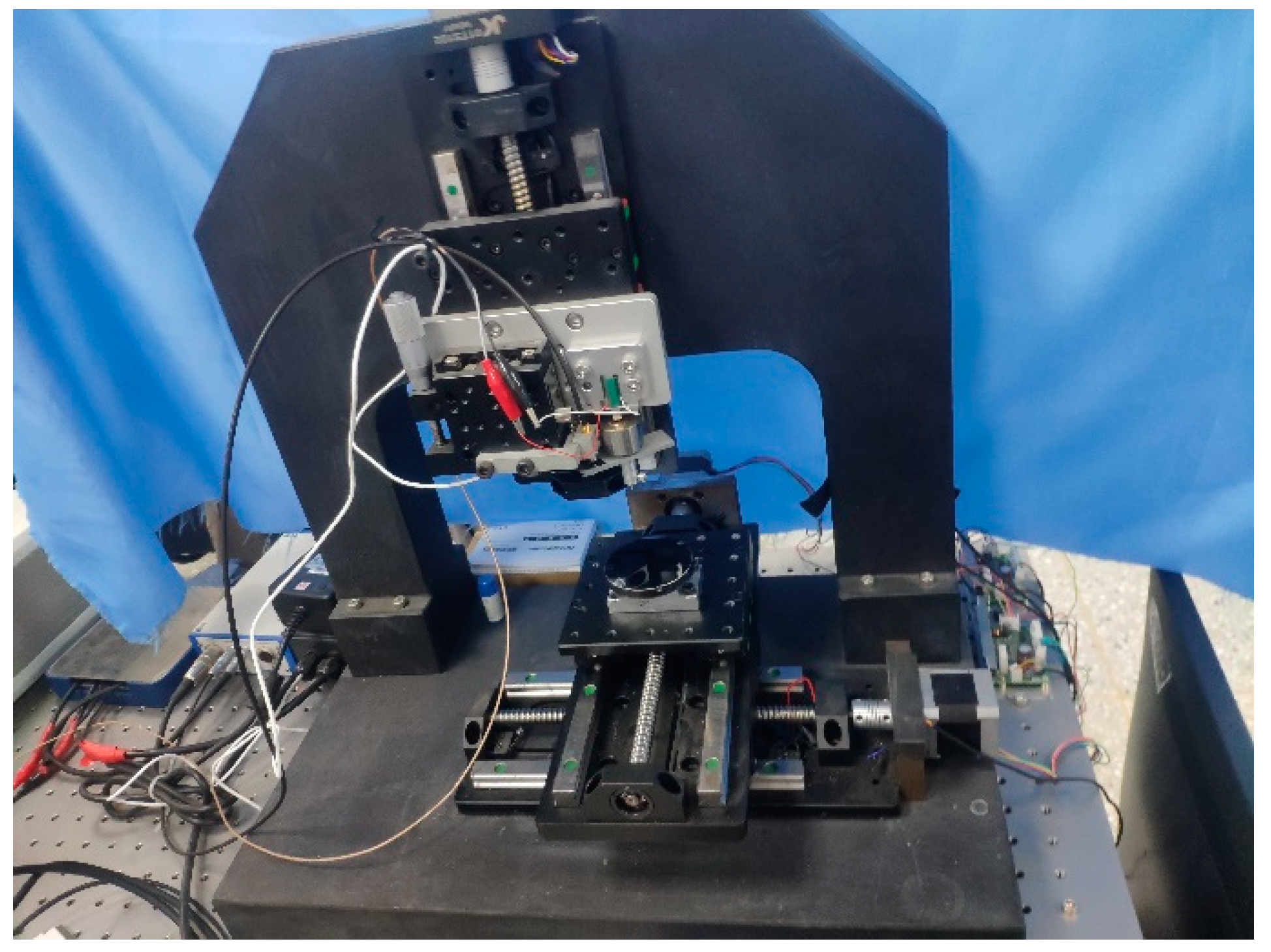
The purpose of nanoindentation experiments in this paper is to explore the hardness and elastic modulus of the modified silicon layer, so as to provide an accurate input to Equation (1). As shown in
Figure 3, during the experiment, the nanoindentation experiments were conducted using a nanoindenter with a Berkovich diamond tip with a radius of curvature of 20 nm. The instrument offers a load resolution of less than 10 μN, and noise levels below 25 μN. The maximum load is 500 mN, and it has a displacement resolution of less than 1 nm. During the experiments, the nanoindentation tests were performed on different areas of the sample surface with applied loads of 50 mN, 100 mN, 200 mN, 300 mN, and 500 mN. To ensure data reliability and repeatability, each set of nanoindentation tests was repeated three times.
3.1. Preparation of Test Samples
Nanoindentation experiments have very strict requirements on the surface of materials, and the high quality surface of materials is a crucial factor to ensure the accuracy and repeatability of nanoindentation experiments. Good surface roughness can ensure that the instrument and probe can accurately contact and sense small deformations, which helps to achieve uniform loading, avoid the influence of test point deviation on the measurement of hardness and elastic modulus, and ensure the accuracy of the experiment.
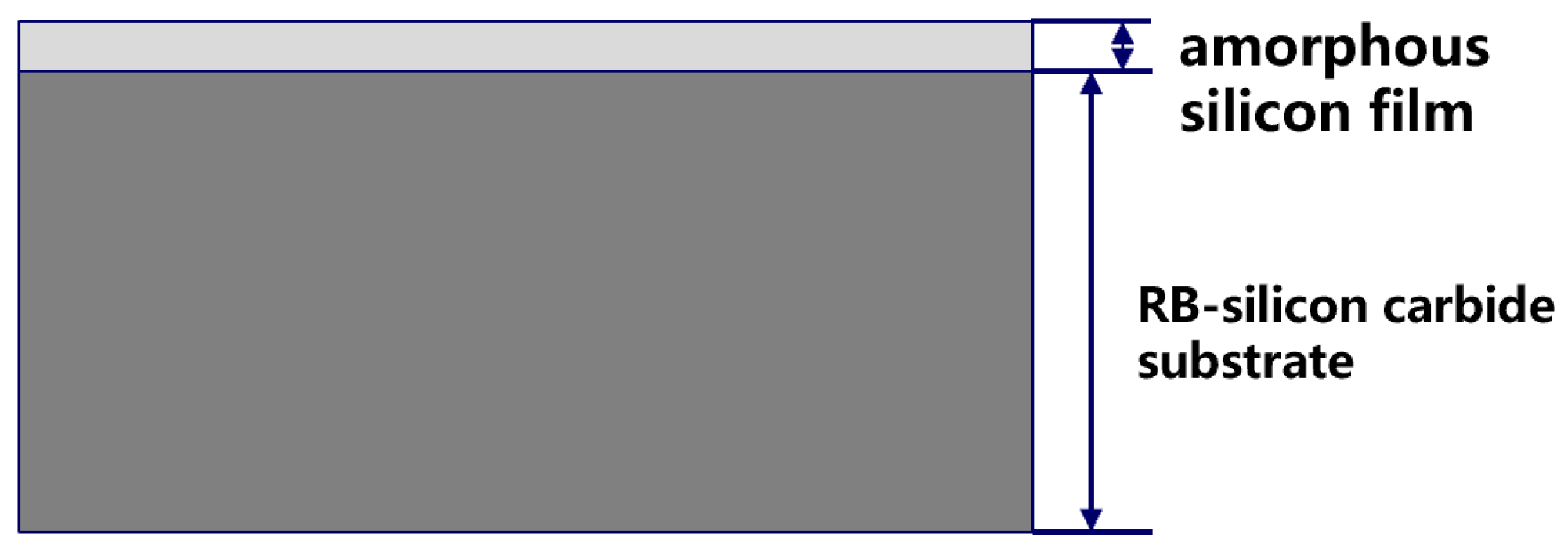
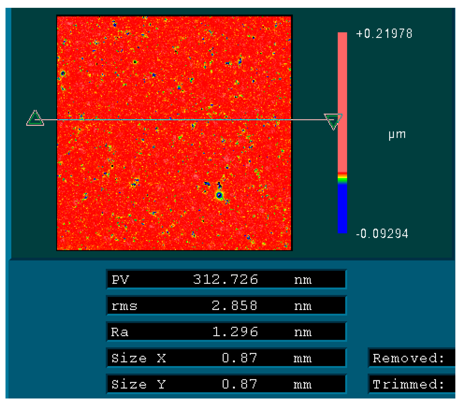
Therefore, the experimental sample used in this paper is the silicon modified Sic described above. The diameter is 60 mm and the thickness of the modified silicon film is 11.7 μm. After a series of milling, grinding, polishing, and other processing procedures, the modified silicon film finally reaches an optical surface roughness Ra of less than 1.3 nm, as shown in
Figure 4.
3.2. Measurement of Hardness and Elastic Modulus
The hardness and elastic modulus of the modified silicon layer were measured using the nanoindentation instrument, and the test results were calculated by the curve of loading and pressing depth.
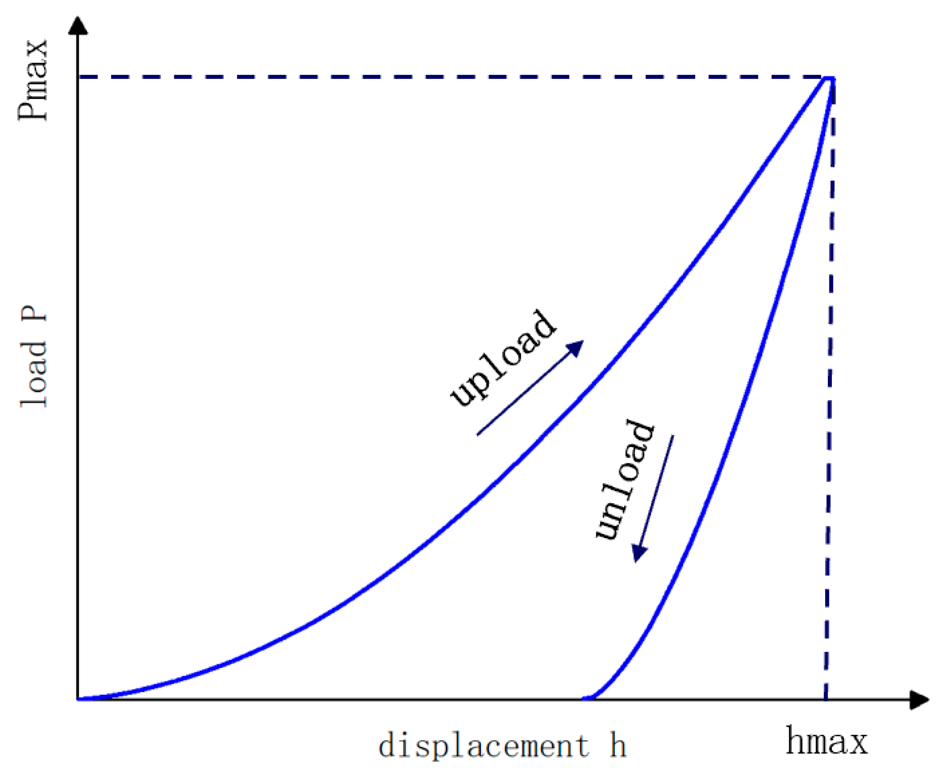
Figure 5 shows the typical load–displacement curve in the nanoindentation test. P is the pressing load; hmax is the maximum depth of indentation. Pmax is the maximum indentation load.
As shown in
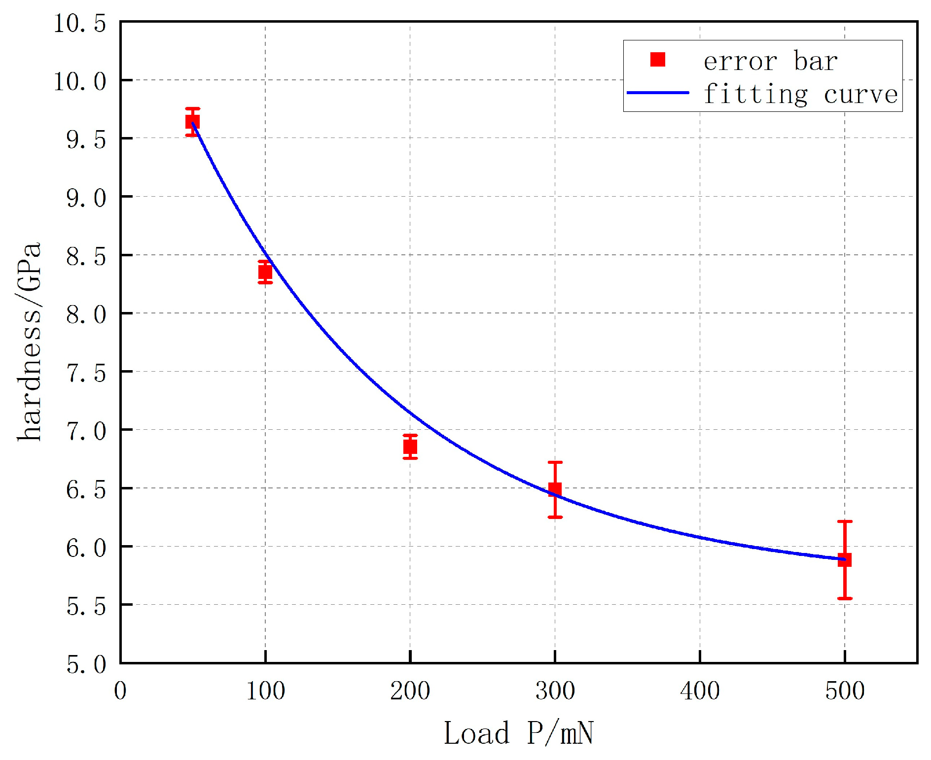
Table 1, the hardness values corresponding to the average results from three experiments for each load of 50 mN, 100 mN, 200 mN, 300 mN, and 500 mN are 9.64 GPa, 8.35 GPa, 6.85 GPa, 6.49 GPa, and 5.88 Gpa. As shown in
Figure 6, with the increase in load, the pressing depth becomes deeper, and the hardness of the material gradually decreases. It can be seen that there is a size effect of silicon-modified Sic [
15]. Through data fitting, it is found that the hardness decreases exponentially with the increase of applied load. The relationship between the hardness and load is described as follows:
where H is the hardness of the material, and P is the load.
In the five sets of experiments, different loads of 50 mN, 100 mN, 200 mN, 300 mN, and 500 mN were applied, and each set was tested three times, with the averages yielding the corresponding elastic modulus values of 126.63 GPa, 123.64 GPa, 126.11 GPa, 143.26 GPa, and 156.81 GPa. With the increase in applied load, the pressing depth gradually deepens. To test the elastic modulus of materials using the nanoindentation method, it is necessary to control the scratch depth to 10% of the film thickness [
16], so that the measured elastic modulus value is more accurate. In this paper, the thickness of the modified silicon film is 11.7 μm, so the average elastic modulus under 50 mN, 100 mN, and 200 mN is selected as the elastic modulus of the modified silicon layer, and the elastic modulus of the modified silicon layer is 125.46 Gpa.
3.3. The Relationship between Indentation Depth and Load
The relationship between the indentation depth and load during the hardness test, as shown in
Figure 7, reveals that there is no fluctuation in the load curve within the indentation range of 0–500 mN. When the maximum indentation load reaches 500 mN, the curve demonstrates excellent continuity. With increasing load, the indentation depth of brittle materials exhibits a power-law growth, and the relationship between the indentation depth and load is as follows:
where d is the indentation depth.
Upon finding the critical load for the plastic-to-brittle transition point and then inserting this load value into Equation (3), one can obtain the plastic removal depth.
4. Nanoscratch Experiments
In the process of mirror fabrication, the removal mechanism of brittle material and the microstructure of the material have a great influence on its local deformation and subsequent removal. In the process of polishing the mirror, the abrasive used is cerium oxide, as shown in
Figure 8 (This image is provided by Universal Optics, its manufacturing address is New York, NY, USA), and its shape is similar to the square cone. In order to better investigate the abrasive behavior in the process of machining, we use the nanoscratch instrument to conduct scratch experiments. Using a standard Vickers indenter with the same shape as the abrasive, the nanoscratch experiment results in the removal and deformation of the material, similar to the effect of abrasive particles when rubbed against a surface. By observing the deformation, cracking, and removal of the material during the scratch process, the behavior of the material under local forces can be understood, which provides a simulation for understanding the behavior of abrasive particles.
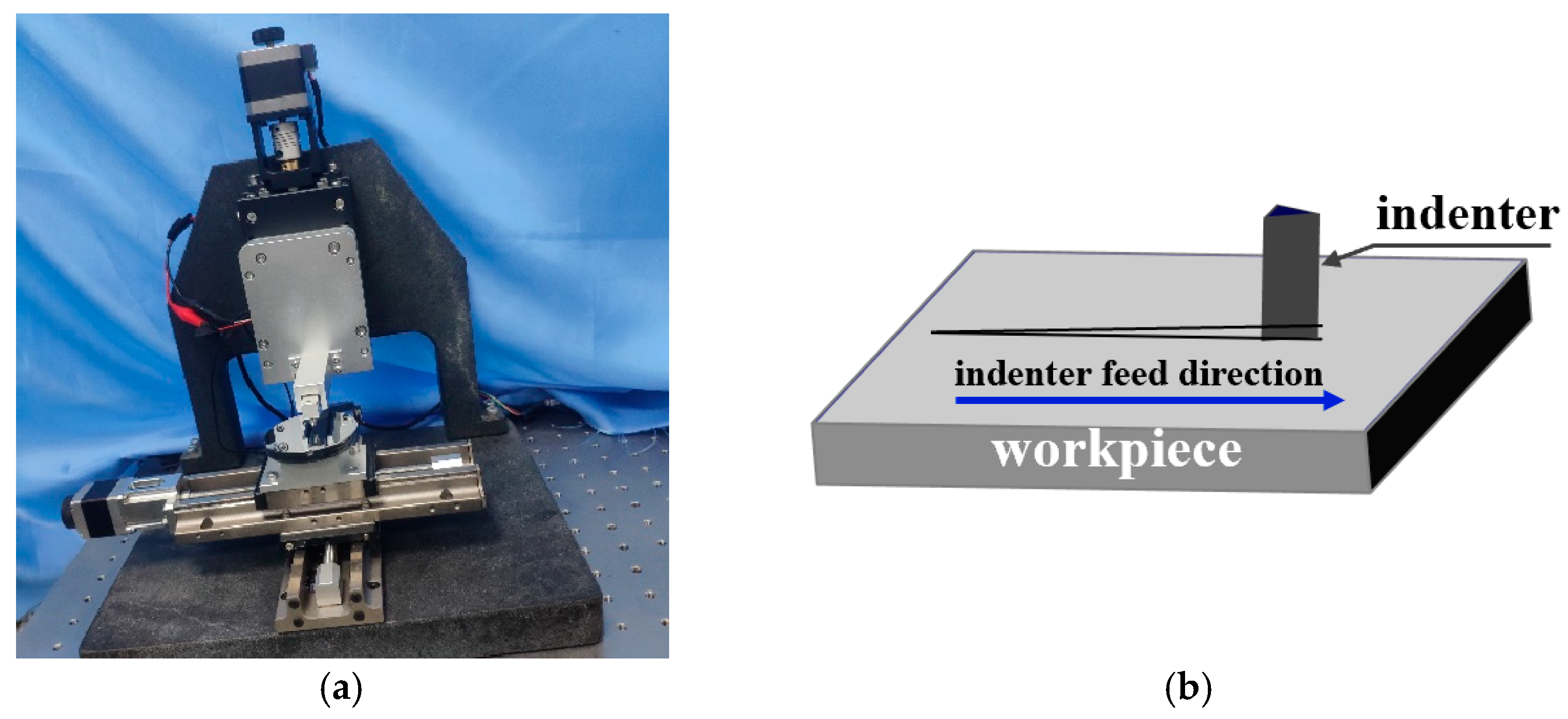
As shown in
Figure 9a, the experimental equipment for the nanoscratch tests included a nanoindenter with a standard Vickers indenter. The load range was 1–1000 mN with a load resolution of 30 μN, and the noise level was less than 0.1 mN. The goal of the nanoscratch experiment was to find the critical point of the material’s brittle-to-plastic transition and determine the critical load for this transition. This critical load was then used in Equation (3) to calculate the critical depth for plastic zone removal. During the experiments, the nanoscratch tests were performed on different regions of the sample surface at loading speeds of 2 mN/s, 4 mN/s, 6 mN/s, 10 mN/s, 16 mN/s, and 20 mN/s (corresponding to maximum loads of 100 mN, 200 mN, 300 mN, 500 mN, 800 mN, and 1000 mN). The scratch speed was 10 µm/s, and the scratch length was 500 µm. Indenter tip feed direction is shown in
Figure 9b. The normal force gradually increased. To ensure the reliability and repeatability of the experimental data, each indentation was performed three times.
4.1. Critical Load for the Plastic-to-Brittle Transition Point
Figure 10,
Figure 11 and
Figure 12 display the surface morphology of the silicon-modified Sic after nanoscratching under different loads. These images were observed at a magnification of 943× using an optical microscope.
Figure 10a–c are scratch morphology images corresponding to the load ranges of 0–100 mN, 0–200 mN, and 0–300 mN, respectively. From the images, it can be observed that in the initial stages of scratching with a lower load, the scratch depth is shallow. As the load increases, the scratch depth gradually increases, and the surface remains smooth without cracks or debris. At this point, the removal mechanism on the surface of the silicon-modified Sic is plastic removal.
Figure 11a,b are scratch morphology images corresponding to load ranges of 0–500 mN and 0–800 mN, respectively. From these images, it can be observed that as the scratching process progresses and the load gradually increases, the scratch depth further increases. The material’s surface clearly exhibits signs of plastic pile-up without the presence of debris. At this point, the removal mechanism on the material’s surface begins to transition from plastic removal to brittle removal. The surface of the silicon-modified Sic is now in a state of coexisting plastic and brittle removal.
Figure 12a,b represent the load vs. time curves and scratch morphology images corresponding to a load range of 0–1000 mN during the scratching process. In the initial stages of scratching, the curve is relatively flat and without fluctuations. As the load increases, material accumulates on both sides of the scratch, indicating a plastic removal mechanism. At 886 mN, the curve begins to exhibit fluctuations, signifying a critical transition point from plastic to brittle removal, known as the material’s plastic-to-brittle transition point. Subsequently, the curve shows increasing oscillations, and as the penetration depth exceeds the critical depth, the material’s surface experiences debris generation and damage, transitioning to complete brittle removal.
4.2. Calculation of the Plastic Removal Depth
Through the nanoscratch experiments, the critical load for the plastic-to-brittle transition on the surface of the silicon-modified Sic was determined to be 886 mN. Upon inserting this value into Equation (2), the material’s hardness during the plastic-to-brittle transition is calculated to be 5.26 GPa. Since there is no equipment available to measure the fracture toughness of the modified silicon layer, a value of 2.0 MPa·√m is used as the fracture toughness of the silicon-modified layer, which can vary depending on the specific experimental and testing conditions as well as factors such as temperature, crystal orientation, sample geometry, and more [
17]. Using this value, Equation (1) yields a plastic removal depth of 2.71 µm for the silicon-modified layer. By substituting the critical load of 886 mN into Equation (3), the plastic removal depth for the silicon-modified layer is calculated to be 2.95 µm.
4.3. Observing the Scratch Depth Using an Atomic Force Microscope
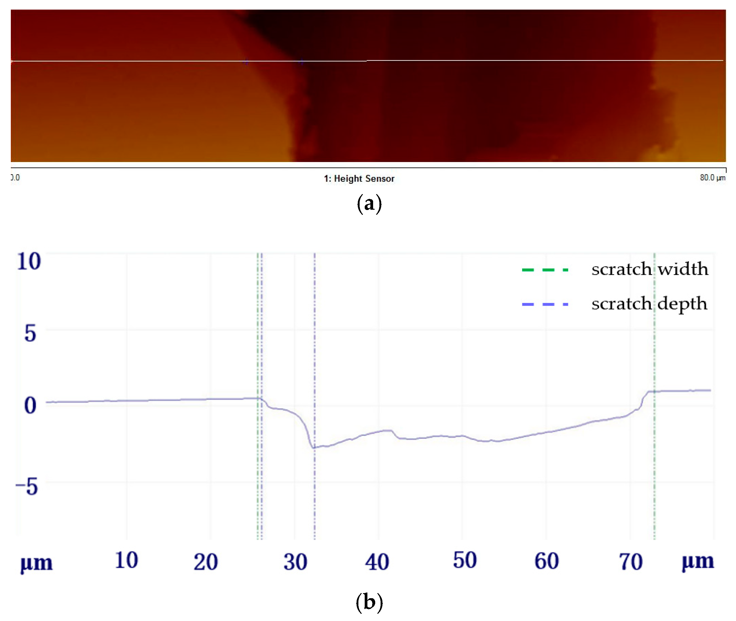
Using an atomic force microscope to observe the scratch depth near 886 mN, from
Figure 13 and
Table 2, it can be seen that the lowest point of the scratch depth is 3.12 μm at this load.
5. Discussion
Table 3 shows the plastic removal depth of the surface of monocrystalline silicon and the critical pressure of the plastic-to-brittle transition point on the surface of Sic, using a nanoindentation test. At present, there is a lack of research on the plastic removal depth and critical pressure of silicon-modified Sic. In this paper, we plated a modified silicon film on the surface of Sic using electron beam evaporation, and studied the plastic removal depth and the critical pressure of the plastic-to-brittle conversion of the combined surface. It is a new breakthrough for the processing of silicon-modified Sic surfaces and has very important guiding significance. According to the theoretical calculation and experimental test results, the method proposed in this paper to calculate the pressing depth by the critical pressure of the plastic-to-brittle transition point of the material to obtain the plastic removal depth and the critical pressure of the brittle plastic transition point is effective.
In order to obtain a high-quality optical surface, we tested this material, but the research in this paper also has shortcomings. First of all, our understanding of the principle of nanoindentation and nanoscratch is not deep enough. Our main purpose is to obtain the plastic removal depth and critical pressure. Secondly, we only tested the silicon-modified Sic material using electron beam evaporation coating, which lacks universality.
In summary, we determined the plastic removal depth and critical pressure of a silicon-modified Sic surface. In the future, we will carry out polishing experiments on the silicon-modified layer to further verify the results of this paper.
6. Conclusions
Through nanoindentation testing, it was determined that the hardness of the silicon-modified Sic surface decreases as the applied load increases, with a hardness of 5.26 GPa at the critical point of the plastic-to-brittle transition. The average elastic modulus was found to be 139.25 GPa, and the indentation depth increased exponentially with increasing load. The theoretical depth, calculated using the critical depth formula, was 2.71 μm. Through an analysis of the load–time curve, the critical load for the plastic-to-brittle transition point was identified as 886 mN. Using the relationship between the indentation depth and load, the plastic removal depth was calculated to be 2.95 μm. Finally, the measurements taken with an atomic force microscope near the critical point of the plastic-to-brittle transition revealed a scratch depth of 3.12 μm. The relative error between the measured value and calculated value is less than 5%. This study provides important guidance for optimizing the parameters of high-quality surface processing.
