High Sensitivity Hydrogen Sensor via the Coupling of Tamm Plasmon Polaritons and Defect Mode


1
Infrared Optoelectronics Laboratory, School of Intelligent Engineering, Henan Institute of Technology, Xinxiang 453003, China
2
Henan Key Laboratory of Infrared Materials & Spectrum Measures and Applications, School of Physics, Henan Normal University, Xinxiang 453007, China
*
Author to whom correspondence should be addressed.
Chemosensors 2024, 12(4), 67; https://doi.org/10.3390/chemosensors12040067
Submission received: 9 March 2024
/
Revised: 11 April 2024
/
Accepted: 17 April 2024
/
Published: 18 April 2024
(This article belongs to the Section Nanostructures for Chemical Sensing)
Abstract
:Optical hydrogen sensors offer high sensitivity, high accuracy, and non-invasive sensing capabilities, making them promising devices in various fields, including the construction of hydrogen fuel cells, storage and transportation, and aerospace. However, to achieve better sensitivity and faster reaction times, such sensors are often constructed as nano-arrays or nano-gratings, leading to increased manufacturing costs and complexity. In this study, we propose and demonstrate a highly sensitive hydrogen sensor based on a multilayer structure. The proposed structure consists of a Pd metal film and a photonic crystal with a defect layer, in which the photonic crystal is designed by an alternating arrangement of Ta2O5 and SiO2, and the material comprising the defect layer is SiO2. With a sensitivity of up to 16,020 at 670 nm, the proposed sensor relies on the coupling of Tamm plasmon polaritons and defect modes. The electric field distribution inside the structure is also provided in order to reveal its physical mechanism. Furthermore, we investigate the effects of the thickness of the defect layer and the angle of incident light on the sensor’s performance. The study results show that the sensor has good fault tolerance in either scenario. The findings of this study open up new possibilities for hydrogen sensor applications.
1. Introduction
Hydrogen, a clean and sustainable energy source, offers numerous advantages, such as high energy efficiency and environmental friendliness. It can be obtained through water decomposition [1,2,3,4]. Furthermore, hydrogen serves as a significant chemical feedstock, particularly for processes such as crude oil hydrogenation and ammonia synthesis [5]. However, hydrogen is both colorless and odorless in the atmosphere, making it imperceptible to human senses. Its flammability and the explosive risk linked to hydrogen concentrations within the range of 4% to 76% in the atmosphere [6] pose potential hazards, including leakage, combustion, and explosion during the various stages of hydrogen production, storage, transportation, refilling, and usage. Although current hydrogen sensors on the market rely on electrical sensing, such as catalytic sensors, thermal conduction sensors, electrochemical sensors, and resistive sensors [7], these electrical sensors are susceptible to electromagnetic interference and may trigger sparks, leading to explosions. In contrast, optical hydrogen sensors are inherently immune to electromagnetic interference and offer the advantage of distributed and multiplexed monitoring, making them more suitable for practical applications. While fiber optic sensors are established optical hydrogen-sensing technologies, their adoption is hampered by complex processing requirements and a lack of mature signal demodulation and detection systems [8].
Localized surface plasmon resonance (LSPR) of metal nanostructures has gained substantial attention as a potential sensing mechanism to be used in hydrogen detection. LSPR’s high sensitivity to the surrounding refractive index enables LSPR-based hydrogen sensors to exhibit exceptional sensitivity and rapid response [9]. Metal nanostructured hydrogen sensors based on LSPR can be divided into the following two categories: nano-array hydrogen sensors [10,11,12,13] and nanodisc hydrogen sensors [14,15,16,17,18]. Poyli et al.’s multiscale theoretical modeling of the plasmonic sensing of hydrogen uptake in palladium provides a robust theoretical foundation for further research in this domain [19]. Yang et al. demonstrated the preparation of Au–Pd hetero-oligomer nanoparticle arrays using reconstructable mask lithography (RML), highlighting the potential of oligomers composed of strong plasmon materials (Au) and specific hydrogen-sensitive materials (Pd) for enhancing hydrogen sensing [13]. Strohfeldt et al. fabricated Pd–Au nanodiscs with different stacking configurations via colloidal hole–mask lithography, revealing that direct-contact Pd–Au nanodiscs exhibited effective hydrogen sensing, with the sensing effect varying based on the stacking method used [18].
Tamm plasmon polaritons (TPPs) are surface plasmons confined between distributed Bragg reflectors (DBRs) or one-dimensional photonic crystals (PhCs) and metal layers [20,21]. In comparison with LSPR, TPP inherits the advantages of LSPR while also offering benefits like direct excitation, low propagation loss, and simpler large-area preparation. The design and fabrication of a TPP hydrogen sensor by Yu Sheng et al. demonstrate the potential of TPP-based sensing in the visible wavelength range, opening up new possibilities for hydrogen detection [22]. Although research on PhCs is relatively advanced, there is limited exploration of TPP hydrogen sensing. Consequently, this form of sensing represents a promising avenue for further research.
One-dimensional photonic crystals, renowned for their exceptional photonic band gap (PBG) characteristics, have captured the interest of photonic researchers [23,24,25,26,27]. The high design flexibility, ease of preparation, and superior optical performance of PhCs position them as promising options for advanced gas sensors. Photonic crystals are created by periodically arranging dielectric materials, allowing effective control over light propagation. As a result, PhCs find applications in sensors, filters, polarizers, switches, and communications [28,29,30]. When applying photonic crystals, the artificial creation of defects within the structure is common, resulting in photonic localization. These defects can involve materials with specific refractive indices or simply cavities that interrupt continuous photon propagation within the nearby periodic structure [31,32]. The formation of energy bands at specific wavelengths within the PBG region when photonic crystals have defects explains the filtering phenomenon. However, research on coupling TPP and defect modes for hydrogen sensing remains limited.
In this study, we aim to enhance the hydrogen-sensing capacity of a sensor by introducing defect layers into the structure generating the TPP in order to produce a TPP hydrogen sensor with higher sensitivity. We explore the possibility of utilizing the coupling of TPPs and defect modes to achieve this goal. To accomplish this, we employ the transfer matrix method (TMM) to calculate the reflectance spectra of this structure. Our results indicate that optimizing the coupling between the TPPs and the defect modes can significantly improve the sensitivity of the TPP hydrogen sensor. We believe that the combination of Pd metal layers and photonic crystals with defect layers provides an innovative solution for TPP hydrogen sensors.
2. Theoretical Model
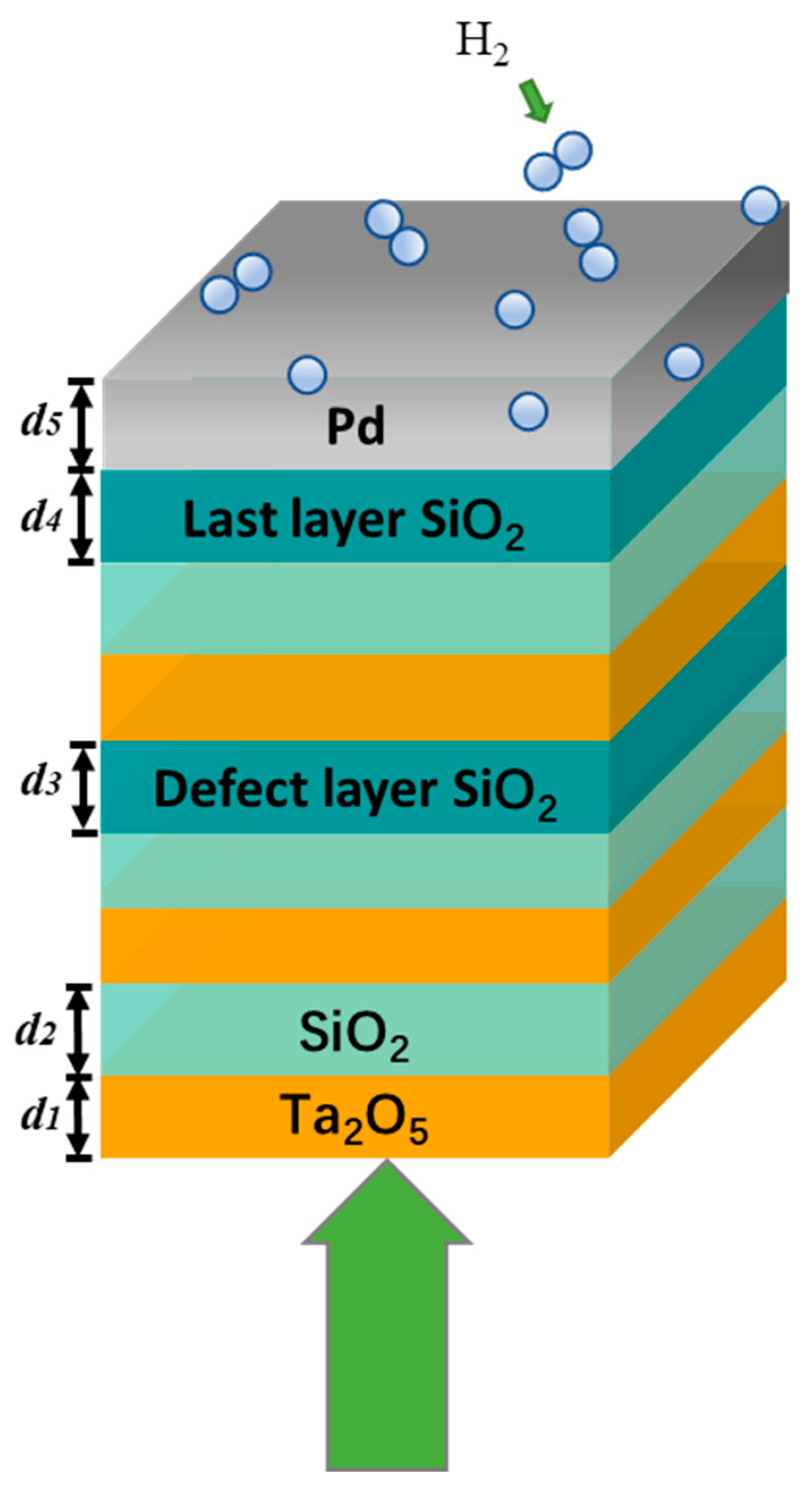
Figure 1 illustrates the schematic structure of the defect layer introduced to the photonic crystal. The system is composed of four parts: a DBR multilayer, a defect layer, a spacer layer, and a metal layer. The DBR multilayer consists of three pairs of high and low refractive index materials Ta2O5 (n1 = 2.11 at 0.792 μm) and SiO2 (n1 = 1.46 at 0.792 μm). The refractive index of Ta2O5 (n1) and SiO2 (n2) was obtained from the models and calculations of Gao and Rodríguez [33,34]. The thicknesses of the Ta2O5 and SiO2 alternating layers in each unit are d1 = 0.0937 μm and d2 = 0.137 μm, respectively, satisfying the Bragg condition (n1·d1 = n2·d2 = λ/4), where λ is the wavelength corresponding to the material refractive index [35]. The defect layer is a SiO2 layer with a thickness of d3 = 0.18 μm located below the fourth layer of the photonic crystal. It works by destroying the periodicity of the photonic crystal and forming a photonic local field, which leads to a coupling of defect modes and TPPs and enhances the local field [36,37]. The material forming the spacer layer is SiO2 (d4 = 0.054 μm), which strengthens the stability and durability of the structure by introducing a layer of SiO2 between the photonic crystal and the metal layer [38]. The key part of the sensor is the Pd metal layer at the bottom (Pd, d5 = 0.07 μm). Its role as a dedicated and highly sensitive hydrogen-sensitive material is crucial for detecting changes in hydrogen concentration. The refractive index of Pd was determined with reference to the results of the model designed and calculations formulated by Rakić et al. [39].
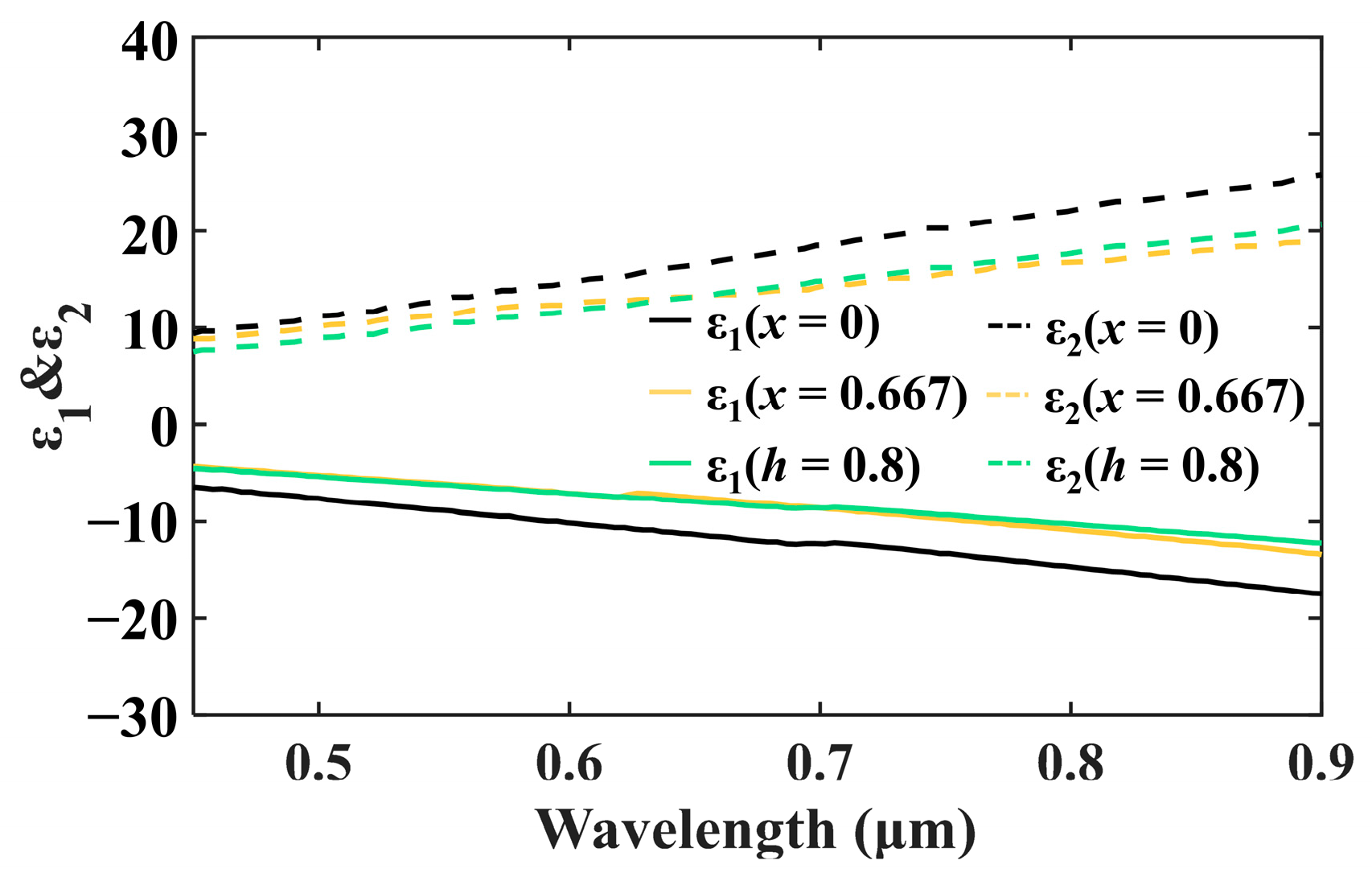
This study delves into the intricate interplay between the defect modes and the TPP, exploring their combined influence on the reflectance of a given structure, alongside variations in sensitivity before and after exposure to hydrogen. Pd-based nanomaterials emerge as promising candidates due to their myriad advantages, including low activation barriers for adsorption, high hydrogen solubility, favorable reaction kinetics, and notable selectivity for hydrogen. Notably, palladium exhibits exceptional hydrogen absorption capabilities, capable of absorbing up to 900 times its volume of hydrogen at ambient temperature, with a reversible hydrogenation process. The overarching aim of this study is to meticulously track the shifts in the optical properties of palladium prior to and following hydrogen absorption, crucial for effective hydrogen detection. Previous investigations have yielded empirical equations elucidating the influence of hydrogen absorption on dielectric functions, particularly at hydrogen concentrations of 0 vol% and 4 vol% [9]:
where denotes the permittivity when the atmosphere is hydrogen with a concentration of c%, while signifies the initial permittivity of pristine Pd in the absence of hydrogen. Additionally, the coefficient h(c%) is associated with the hydrogen concentration (c%) in a non-linear manner. Specifically, h(0%) equals 1, and h(4%) equals 0.8, corresponding to the hydrogen concentrations of 0 vol% and 4 vol%, respectively.
Furthermore, Poyli et al. proposed a theoretical model for plasma sensing after hydrogen absorption by Pd, investigating the use of the Brueggemann effective medium definition to explain the biphasic nature of the Pd–H system [19]. It is proposed that when Pd is exposed to hydrogen, it can absorb hydrogen from the surface and decompose the hydrogen molecules into hydrogen atoms, which subsequently enter the lattice of Pd metal and palladium hydride (Pd–H), which can affect the dielectric functions of Pd-based hydrogen sensors [40]. Palladium hydride (PdHx), theoretically, is a mixture of two phases, α and β. In the α phase, the concentration of H atoms is low, and the dielectric properties are comparable to pure Pd (PdHx = 0). In the β phase, the H concentration is high, and the dielectric properties are comparable to PdHx = 1 [41]. But in fact, when x < 0.01, PdHα will be in solid solution form due to the random distribution of hydrogen occupying it; when x < 0.6, the octahedral lattice hydride PdHβ will be formed; and secondly, for bulk Pd, the transformation of PdHα to form PdHβ occurs only under the condition that the concentration of H2 is 1%, whereas H saturation in the β-phase occurs at x ≈ 0.667. The ab initio dielectric functions of the α and β phases can be weighted and averaged according to the Bruggeman effective medium approximation to construct the corresponding effective dielectric function εeff(x) [42,43]. Specifically, the following formula can be used:
where εα and εβ are the dielectric functions of α and β phases, as well as fβ being the phase of the saturated β phase. By employing this approach, the optical behavior of the entire α and β phase composite system can be elucidated, thereby enabling the determination of the optical characteristics pertaining to the PdHx system.
According to Figure 2, we have analyzed two different methods for describing the dielectric functions of Pd after hydrogen absorption. The black curve represents the dielectric function of pure palladium as measured by the ellipsometry method (the solid part is represented by a solid line and the imaginary part by a dashed line). Based on the measured dielectric function of pure palladium, we calculated the dielectric functions at a hydrogen concentration of 4 vol% in ambient nitrogen using Equation (1) and obtained the green curve in Figure 2 (the solid part is represented by a solid line and the dashed part by a dotted line). At the same time, we also calculated the Pd dielectric functions after hydrogen absorption saturation according to Equation (2) (where x is set to 0.667). The calculated results are shown as the yellow curve values in Figure 2 (the real part is represented by the solid line and the imaginary part by the dashed line). It is noteworthy that that the yellow and green curves calculated by these two methods almost coincide, thus verifying their feasibility in characterizing metallic palladium plasma sensing. Equation (2) can be used to describe the change in the dielectric functions of Pd after hydrogenation in a re-nitrogen environment with the passage of 4 vol% hydrogen.
The reflectance spectra, sensitivity, and electric field diagram calculated in this design were all obtained using the TMM [44,45]. Widely recognized for its robustness and accuracy, the TMM is a computational technique that allows for the meticulous analysis of optical properties in complex systems. By leveraging the TMM, we ensure a comprehensive and precise understanding of the interplay between various components within the structure under investigation, thereby enhancing the depth and rigor of our analysis.
3. Results and Discussion
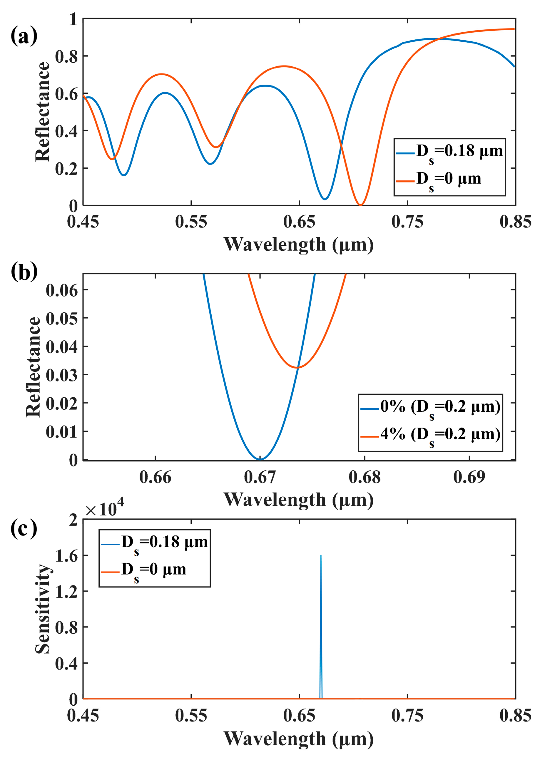
Figure 3 illustrates a comparison between the reflectance spectra of the proposed structure before and after the introduction of the defect layer, where the defect layer consists of SiO2 with a thickness of 0.18 μm (Figure 3a). The trends of change in the two reflectance spectra are similar, and it is evident that both spectra exhibit pronounced near-zero resonance dips. This observation suggests that the introduction of the defect layer did not disrupt the excitation of the TPP within this configuration. Upon the incorporation of the defect layer, a near-zero resonance dip emerges at 670 nm within the reflectance spectra, and this resonance dip experiences a blue shift compared to the spectra obtained without the defect layer.
To assess the structure’s hydrogen-sensing performance, we compared the reflectance spectra of the TPP structure with the defect layer before and after the introduction of hydrogen (Figure 3b). We magnified the vertical axis of the reflectance spectra within the range of 0 to 0.07 to observe the changes in reflectance spectra resulting from the introduction of hydrogen. As depicted in Figure 3b, following exposure to 4 vol% H2, the resonance dip undergoes a red shift of 4 nm, and the reflectance at the resonant wavelength escalates from 3.25 × 10⁻⁶ to 5.21 × 10⁻². In order to characterize the detection performance of the designed structure more intuitively, we calculate the responsivity before and after the passage of hydrogen and define it as the sensitivity of this sensor, i.e., Equation (3), where R1 and R0 represent the reflectance after exposure to hydrogen and the initial state [22], respectively. The computed sensitivity results are presented in Figure 3c. With the integration of a 0.18 μm defect layer into the photonic crystal, the structure’s sensitivity escalates from 31 to 16,020, representing an augmentation of nearly 516 times. Consequently, the inclusion of the defect layer proved instrumental in optimizing the resonance dip and consequently enhancing sensitivity.
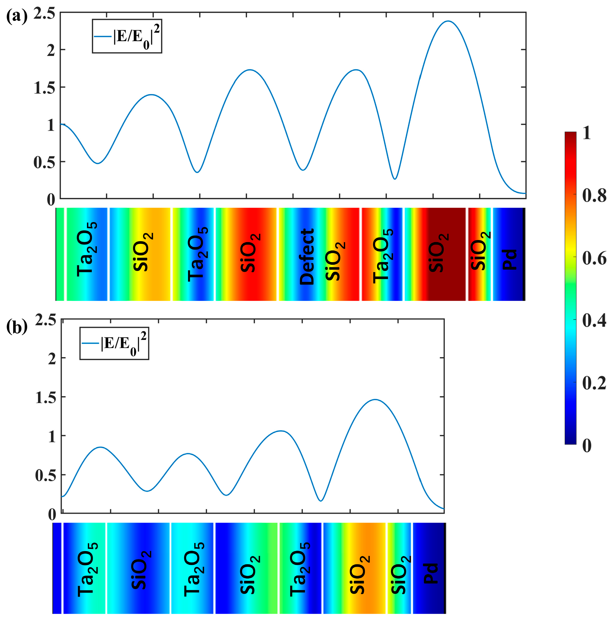
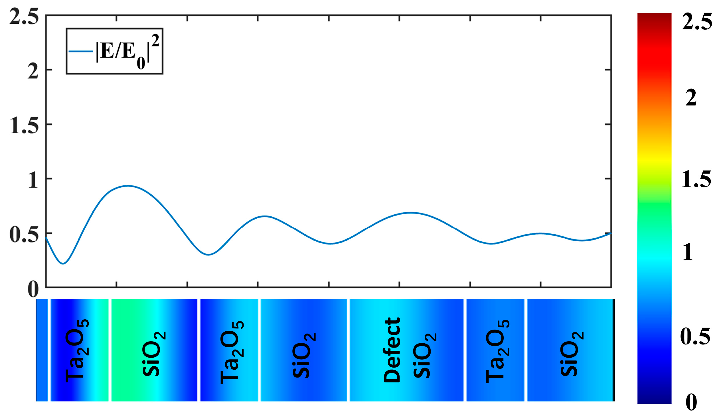
In order to better understand the coupling between the defect modes and TPPs generated after the introduction of defect layer, we calculated the electric field diagram at the resonance dip of 670 nm when the defect layer was not introduced and when the thickness of the defect layer was 0.18 μm, as shown in Figure 4. Line electric field and color electric field diagrams before and after the introduction of the defect layer were plotted to compare the strength of the electric field in each layer more clearly. The TPP is an interface state, and the energy of the electric field is highly concentrated near the interface. For both structures, the TPP is excited at the location of the spacer layer, generating a strong electric field.
In general, the electric field of the structure without the defect layer only has two bands with higher field strengths (Figure 4a). The strongest energy band is located at the interface between the DBR pair and the metal layer, where the TPP is generated, resulting in a strong localized field [46]. The other energy band with higher field strength is located at the interface between the two materials of the last pair of Bragg reflectors. In contrast, the electric field of the structure with the defect layer shows three bands with higher field strengths, with one of the higher field strengths observed at the position of the defect layer (Figure 4b). This is because the defect layer forms energy bands while destroying the photonic crystal, thus creating a local field that hinders the propagation of photons and reduces the reflectance. By analyzing the electric field distribution of the structure, it was found that the introduced defect layer forms a defect mode and couples with the TPP, enhancing the local field of the structure [47], which eventually greatly improves the hydrogen-sensing sensitivity of the structure.
In this study, we also explored the excitation of defect modes and the coupling between TPPs and defect modes. To this end, we removed the Pd metal layer and the spacer layer and focused solely on the photonic crystal with the defect layer. Figure 5 displays the normalized electric field distribution inside the structure at a wavelength of 670 nm, with a defect layer thickness of 0.18 μm. Notably, the electric field intensity still exhibits an increase in the region of the defect layer, even without the presence of the TPP. This implies that the defect mode can be excited in the absence of the TPP. The comparison between Figure 4a and Figure 5 reveals that the magnetic field intensity near the defect layer in Figure 4a is considerably higher than that of Figure 5. This finding indicates that when the TPPs and defect modes are excited concurrently, they can couple with each other, resulting in the enhancement of TPPs and defect modes separately.
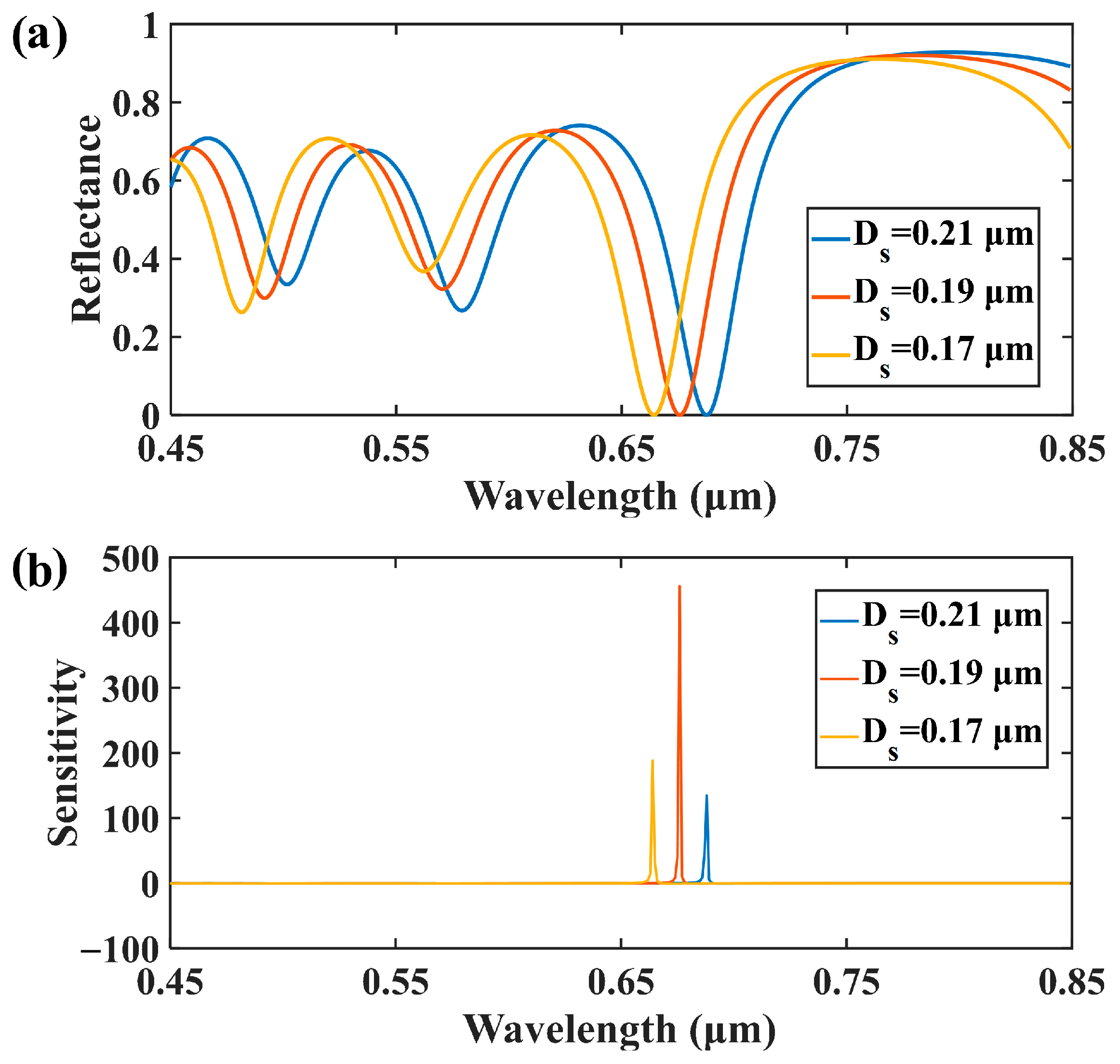
Since the thickness of the defect layer has a significant effect on this structure, the main focus of this study was to analyze the influence of the thickness of the defect layer on the TPP structure. Specifically, we calculated the reflectance spectra of the defect layers with thicknesses of 0.21, 0.19, and 0.17 μm (Figure 6a). It can be observed from the figure that the reflectance spectra all achieve good near-zero resonance dips in the visible band when the thickness of the defect layer is between 0.17 and 0.21 μm. In addition, as the thickness of the defect layer increases, the trough of the reflectance spectra is red shifted. This is because the change in defect layer thickness affects the intrinsic loss of the defect layer, which leads to a shift in the critical coupling wavelength [48]. Finally, the sensitivity of the defect layer was calculated using Equation (3) for the corresponding thickness (Figure 6b). It can be observed that the structure still has sufficient sensitivity performance in the defect layer thickness range of 0.17–0.21 μm, which provides a good margin of error for the preparation of the structure. Since the thickness of the defect layer is not linearly related to the variation in the hydrogen-sensing sensitivity of the structure, the structure requires a high degree of accuracy in the thickness of the defect layer. The design of this structure maintains good sensitivity in the defect layer thickness range of 0.17–0.21 µm, which also minimizes manufacturing difficulties.
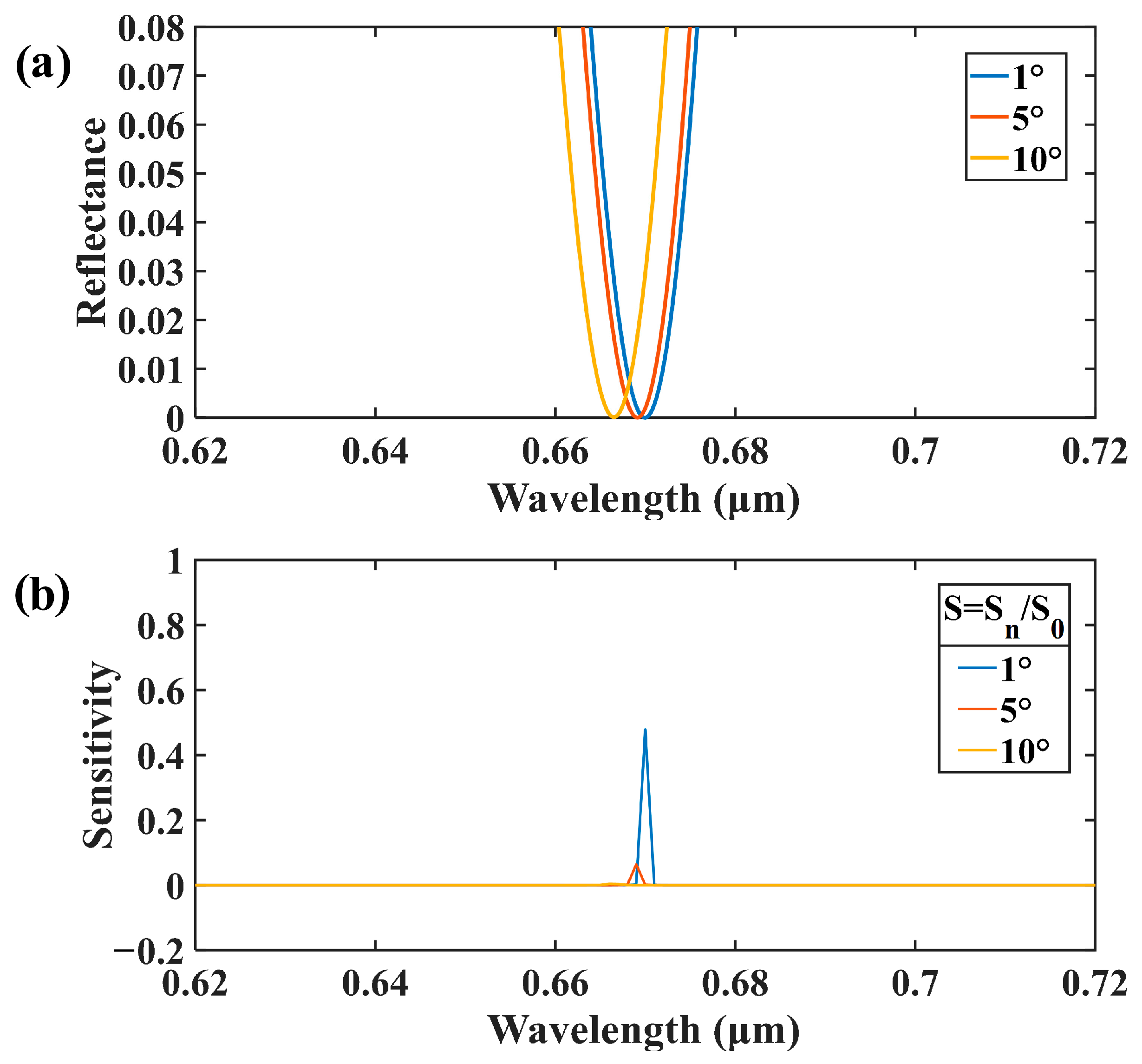
In practical applications, the sensing performance of sensors is also affected by the angle of incidence of light. Next, we will explore the relationship between the angle of incidence of light and the sensitivity of the TPP hydrogen sensor, as shown in Figure 7. In order to highlight the variations in the near-zero resonance dips of the reflectance spectra at different angles, we narrowed the calculated wavelength range. As shown in Figure 7a, the reflectance spectra of the structure were calculated in the wavelength range of 0.62 to 0.72 μm with the introduction of a defect layer of 0.18 μm thickness. It can be clearly seen that the resonance dips of the TPP hydrogen sensor exhibit good zero reflectance in all angular ranges from 1° to 10° and that they are slightly blue shifted with angle change.
To facilitate comparison with the sensitivity when the incident light is perpendicular to the structure, the sensitivity was normalized for incident angles of 1°, 5°, and 10°. That is, S = Sn/S0, where Sn represents the sensitivity when the incident angle changes by n° and S0 indicates the sensitivity at vertical incidence. The normalized sensitivity at different incident angles is shown in Figure 7b, where it can be observed that when the incident light deviates from 1°, the sensitivity is half that of perpendicular incidence, which is about 7600. At this point, the structure still has relatively high hydrogen-sensing sensitivity. The sensitivity of the TPP hydrogen sensor is 75.4 when the incident angle deviates by 10°, which is significantly lower compared with the sensitivity at vertical incidence. However, it is still twice as sensitive as the sensitivity at vertical incidence of the TPP structure without the defect layer. In addition, the structure still exhibits good sensitivity at an incidence angle of 5°. Combining the above results, it can be seen that the structure with the defect layer introduced still has good sensitivity in the range of incidence angle change from 1 to 10°. This suggests that it has a certain degree of robustness against changes in the angle of incidence and has good sensing performance in the small angle range.
4. Conclusions
In conclusion, we have extensively examined the performance of a hydrogen sensor utilizing a composite structure comprising a Pd metal film and a one-dimensional photonic crystal that integrates a defect layer. This configuration has enabled the realization of a hydrogen sensor with significantly heightened sensitivity, accomplished through the effective coupling of Tamm plasmon polaritons (TPPs) and defect modes. Remarkably, the achieved sensitivity of this structure for hydrogen sensing at the wavelength of 670 nm reaches an impressive 16,020. Our investigation demonstrates the excitation of TPPs between the Pd metal film and the photonic crystal, wherein the coupling of TPPs with the defect mode plays a pivotal role in amplifying local field strength, thereby resulting in a substantial increase in sensitivity. In this study, we also present detailed reflectance spectra and sensitivity profiles for a structure with diverse defect layer thicknesses. Notably, it was established that the structure maintains its high sensitivity within the defect layer thickness range of 0.17 to 0.21 μm. Furthermore, we also investigated the impact of changes in incident light angle on the hydrogen-sensing performance of this structure. The findings reveal that the structure retains its high sensitivity even with fluctuations in the incident light angle within the 0–10° range. This study demonstrates the potential of integrating a Pd metal film with a photonic crystal that has a defect layer to enhance the local field and improve the hydrogen-sensing sensitivity. Moreover, it exhibits a certain degree of fault tolerance in terms of the thickness of the defect layer and the angle of incident light. This structure presents promising applications in the field of hydrogen sensing.
Author Contributions
Conceptualization, F.Z.; methodology, F.Z.; software, W.Y.; validation, F.Z., W.Y. and J.Z.; data F.Z. and W.Y.; writing—original draft preparation, F.Z.; resources, F.Z.; funding acquisition, F.Z. and J.Z. All authors have read and agreed to the published version of the manuscript.
Funding
This study was supported by the National Natural Science Foundation of China (Grant 11274096), the Henan Province Science and Technology Research Project (Grant 192102110198, 232102210187), and the Key Scientific Research Projects of Colleges and Universities in Henan Province (23B210005).
Institutional Review Board Statement
Not applicable.
Informed Consent Statement
Not applicable.
Data Availability Statement
The data presented in this paper can be obtained from the authors upon request.
Conflicts of Interest
The authors declare no conflicts of interest.
References
- Dawood, F.; Anda, M.; Shafiullah, G.M. Hydrogen production for energy: An overview. Int. J. Hydrogen Energy 2020, 45, 847–3869. [Google Scholar] [CrossRef]
- Dincer, I. Green methods for hydrogen production. Int. J. Hydrogen Energy 2012, 37, 1954–1971. [Google Scholar] [CrossRef]
- Sakintuna, B.; Lamari-Darkrim, F.; Hirscher, M. Metal hydride materials for solid hydrogen storage: A review. Int. J. Hydrogen Energy 2007, 32, 1121–1140. [Google Scholar] [CrossRef]
- Turner, J.A. Sustainable hydrogen production. Science 2004, 305, 972–974. [Google Scholar] [CrossRef] [PubMed]
- Ball, M.; Wietschel, M. The future of hydrogen-opportunities and challenges. Int. J. Hydrogen Energy 2009, 34, 615–627. [Google Scholar] [CrossRef]
- Hübert, T.; Boon-Brett, L.; Black, G.; Banach, U. Hydrogen sensors—A review. Sens. Actuators B 2011, 157, 329–335. [Google Scholar] [CrossRef]
- Ai, B.; Sun, Y.J.; Zhao, Y.P. Plasmonic hydrogen sensors. Nano-Micro Small 2022, 18, 2107882. [Google Scholar] [CrossRef] [PubMed]
- Zhang, Y.N.; Peng, H.J.; Qian, X.L.; Zhang, Y.Y.; An, G.W.; Zhao, Y. Recent advancements in optical fiber hydrogen sensors. Sens. Actuators B 2017, 244, 393–416. [Google Scholar] [CrossRef]
- Chen, K.F.; Yuan, D.P.; Zhao, Y.Y. Review of optical hydrogen sensors based on metal hydrides: Recent developments and challenges. Opt. Laser Technol. 2021, 137, 106808. [Google Scholar] [CrossRef]
- Tittl, A.; Mai, P.; Taubert, R.; Dregely, D.; Liu, N.; Giessen, H. Palladium-based plasmonic perfect absorber in the visible wavelength range and its application to hydrogen sensing. Nano Lett. 2011, 11, 4366–4369. [Google Scholar] [CrossRef]
- Xu, F.; Zhang, Z.; Ma, J.; Ma, C.; Guan, B.O.; Chen, K. Large-area ordered Palladium nanostructures by colloidal lithography for hydrogen sensing. Molecules 2022, 27, 6100. [Google Scholar] [CrossRef]
- Luong, H.M.; Pham, M.T.; Guin, T.; Richa, P.M.; Manh, H.P.; George, K.L.; Tho, D.N. Sub-second and ppm-level optical sensing of hydrogen using templated control of nano-hydride geometry and composition. Nat. Commun. 2021, 12, 2414. [Google Scholar] [CrossRef] [PubMed]
- Yang, A.; Huntington, M.D.; Cardinal, M.F.; Masango, S.S.; Van Duyne, R.P.; Odom, T.W. Hetero-oligomer nanoparticle arrays for plasmon-enhanced hydrogen sensing. ACS Nano 2014, 8, 7639–7647. [Google Scholar] [CrossRef] [PubMed]
- Timur, S.; Peter, J.; Christoph, L.; Mikael, K. Directional scattering and hydrogen sensing by bimetallic Pd-Au nanoantennas. Nano Lett. 2012, 12, 2464–2469. [Google Scholar] [CrossRef]
- Wadell, C.; Antosiewicz, T.J.; Langhammer, C. Optical absorption engineering in stacked plasmonic AuSiO2-Pd nanoantennas. Nano Lett. 2012, 12, 4784–4790. [Google Scholar] [CrossRef]
- Silkin, V.M.; Díez Muiño, R.; Chernov, I.P.; Chulkov, E.V.; Echenique, P.M. Tuning the plasmon energy of palladium hydrogen systems by varying the hydrogen concentration. J. Phys. Condens. Matter 2012, 24, 104021. [Google Scholar] [CrossRef] [PubMed]
- Baldi, A.; Narayan, T.C.; Koh, A.L.; Dionne, J.A. In situ detection of hydrogen-induced phase transitions in individual palladium nanocrystals. Nat. Mater. 2014, 13, 1143–1148. [Google Scholar] [CrossRef] [PubMed]
- Strohfeldt, N.; Zhao, J.; Tittl, A.; Giessen, H. Sensitivity engineering in direct contact palladium-gold nano-sandwich hydrogen sensors. Opt. Mater. Express 2015, 5, 2525–2535. [Google Scholar] [CrossRef]
- Poyli, M.A.; Silkin, V.M.; Chernov, I.P.; Echenique, P.M.; Muiño, R.D.; Aizpurua, J. Multiscale theoretical modeling of plasmonic sensing of hydrogen uptake in palladium nanodisks. J. Phys. Chem. Lett. 2012, 3, 2556–2561. [Google Scholar] [CrossRef]
- Sasin, M.E.; Seisyan, R.P.; Kalitteevski, M.A.; Brand, S.; Abram, R.A.; Chamberlain, J.M.; Egorov, A.Y.; Vasil’ev, A.P.; Mikhrin, V.S.; Kavokin, A.V. Tamm plasmon polaritons: Slow and spatially compact light. Appl. Phys. Lett. 2008, 92, 251112. [Google Scholar] [CrossRef]
- Sasin, M.E.; Seisyan, R.P.; Kalitteevski, M.A.; Brand, S.; Abram, R.A.; Chamberlain, J.M.; Egorov, A.Y.; Vasil’ev, A.P.; Mikhrin, V.S.; Kavokin, A.V. RETRACTED: Tamm plasmon-polaritons: First experimental observation. Micro Nanostruct. 2010, 47, 44–49. [Google Scholar] [CrossRef]
- Xu, H.; Wu, P.; Zhu, C.; Elbaz, A.; Zhong, Z.G. Photonic crystal for gas sensing. J. Mater. Chem. C 2013, 1, 6087–6098. [Google Scholar] [CrossRef]
- Zaky, Z.A.; Aly, A.H. Theoretical study of a tunable low-temperature photonic crystal sensor using dielectric superconductor nanocomposite layers. J. Supercond. Nov. Magn. 2020, 33, 2983–2990. [Google Scholar] [CrossRef]
- Zaky, Z.A.; Aly, A.H. Gyroidal graphene/porous silicon array for exciting optical Tamm state as optical sensor. Sci. Rep. 2021, 11, 19389. [Google Scholar] [CrossRef] [PubMed]
- Ye, M.Y.Y.; Xie, Z.; Tang, J.; Ouyang, J.X. Highly sensitive and tunable terahertz biosensor based on optical Tamm states in graphene-based Bragg reflector. Results Phys. 2019, 15, 102779. [Google Scholar] [CrossRef]
- Zaky, Z.A.; Sharma, A.; Alamri, S.; Aly, A.H. Theoretical evaluation of the refractive index sensing capability using the coupling of Tamm-Fano resonance in one-dimensional photonic crystals. Appl. Nanosci. 2021, 11, 2261–2270. [Google Scholar] [CrossRef]
- Wu, F.; Liu, T.; Xiao, S. Polarization-sensitive photonic bandgaps in hybrid one-dimensional photonic crystals composed of all-dielectric elliptical metamaterials and isotropic dielectrics. Appl. Opt. 2023, 62, 706–713. [Google Scholar] [CrossRef] [PubMed]
- Mbakop, F.K.; Djongyang, N.; Ejuh, G.W.; Raïdandi, D.; Woafo, P. Transmission of light through an optical filter of a one-dimensional photonic crystal: Application to the solar thermophotovoltaic system. Phys. B 2017, 516, 92–99. [Google Scholar] [CrossRef]
- Panda, A.; Devi, P.P. Photonic crystal biosensor for refractive index based cancerous cell detection. Opt. Fiber Technol. 2020, 54, 102123. [Google Scholar] [CrossRef]
- Qiao, F.; Zhang, C.; Wan, J.; Zi, J. Photonic quantum-well structures: Multiple channeled filtering phenomena. Appl. Phys. Lett. 2020, 77, 3698. [Google Scholar] [CrossRef]
- Nimtz, G.; Haibel, A.; Vetter, R.M. Pulse reflection by photonic barriers. Phys. Rev. E 2002, 66, 037602. [Google Scholar] [CrossRef] [PubMed]
- Chen, Y.S.; Yang, Z.Y.; Ye, M.J.; Wu, W.H.; Chen, L.H.; Shen, H.J.; Ishii, S.; Nagao, T.; Chen, K.P. Tamm plasmon polaritons hydrogen sensors. Adv. Phys. Res. 2023, 2, 2200094. [Google Scholar] [CrossRef]
- Gao, L.; Lemarchand, F.; Lequime, M. Refractive index determination of SiO2 layer in the UV/Vis/NIR range: Spectrophotomtric reverse engineering on single and bi-layer designs. J. Eur. Opt. Soc-Rapid 2013, 8, 13010. [Google Scholar] [CrossRef]
- Rodríguez-de Marcos, L.V.; Larruquert, J.I.; Méndez, J.A.; Aznárez, J.A. Self-consistent optical constants of SiO2 and Ta2O5 films. Opt. Mater. Express 2016, 6, 3622–3637. [Google Scholar] [CrossRef]
- Deng, C.Z.; Ho, Y.L.; Lee, Y.C.; Wang, Z.Y.; Tai, Y.H.; Zyskowski, M.; Daiguji, H.; Delaunay, J.J. Two-pair multilayer Bloch surface wave platform in the near- and mid-infrared regions. Appl. Phys. Lett. 2019, 115, 091102. [Google Scholar] [CrossRef]
- Timofeev, I.V.; Maksimov, D.N.; Sadreev, A.F. Optical defect mode with tunable Q factor in a one-dimensional anisotropic photonic crystal. Phys. Rev. B 2018, 97, 024306. [Google Scholar] [CrossRef]
- Wu, J.Z.; Li, H.J.; Fu, C.J.; Wu, X.H. High quality factor nonreciprocal thermal radiation in a Weyl semimetal film via the strong coupling between Tamm plasmon and defect mode. Int. J. Therm. Sci. 2023, 184, 107902. [Google Scholar] [CrossRef]
- Zaky, Z.A.; Hanafy, H.; Panda, A.; Pukhrambam, P.D.; Aly, A.H. Design and analysis of gassensor using tailorable Fano resonance by coupling between Tamm and defected mode resonance. Plasmonics 2022, 17, 2103–2111. [Google Scholar] [CrossRef]
- Rakić, A.D.; Djurišic, A.B.; Elazar, J.M.; Majewski, M.L. Optical properties of metallic films for vertical-cavity optoelectronic devices. Appl. Opt. 1998, 37, 5271–5283. [Google Scholar] [CrossRef]
- von Rottkay, K.; Rubin, M. Refractive index changes of Pd-coated magnesium lanthanide switchable mirrors upon hydrogen insertion. J. Appl. Phys. 1999, 85, 408–413. [Google Scholar] [CrossRef]
- Aspnes, D.E. Plasmonics and effective-medium theories. Thin Solid Film. 2011, 519, 2571–2574. [Google Scholar] [CrossRef]
- Ahn, J.S.; Kim, K.H.; Noh, T.W.; Riu, D.H.; Boo, K.H.; Kim, H.E. Effective-medium theories for spheroidal particles randomly oriented on a plane: Application to the optical properties of a SiC whisker-Al2O3 composite. Phys. Rev. B 1995, 52, 15244–15252. [Google Scholar] [CrossRef]
- Garnett, J.C.M. Colours in metal glasses and in metallic films. Philos. Trans. R. Soc. A 1904, 203, 385–420. [Google Scholar] [CrossRef]
- Wu, X.H.; Fu, C.J.; Zhang, Z.M. Influence of hBN orientation on the near-field radiative heat transfer between graphene/hBN heterostructures. J. Photonics Energy 2018, 9, 032702. [Google Scholar] [CrossRef]
- Wu, J.; Wang, Z.M.; Wu, B.Y.; Shi, Z.X.; Wu, X.H. The giant enhancement of nonreciprocal radiation in Thue-morse aperiodic structures. Opt. Laser Technol. 2022, 152, 108138. [Google Scholar] [CrossRef]
- Kaliteevski, M.; Iorsh, I.; Brand, S.; Abram, R.A.; Chamberlain, J.M.; Kavokin, A.V.; Shelykh, I.A. Tamm plasmon-polaritons: Possible electromagnetic states at the interface of a metal and a dielectric Bragg mirror. Phys. Rev. B 2007, 76, 165415. [Google Scholar] [CrossRef]
- Brückner, R.; Sudzius, M.; Hintschich, S.I.; Frob, H.; Lyssenko, V.G.; Leo, K. Hybrid optical Tamm states in a planar dielectric microcavity. Phys. Rev. B 2011, 3, 033405. [Google Scholar] [CrossRef]
- Wu, X.H.; Chen, Z.X.; Wu, F. Strong nonreciprocal radiation in a InAs film by critical coupling with a dielectric grating. ES Energy Environ. 2021, 13, 8–12. [Google Scholar] [CrossRef]
Figure 1.
Schematic diagram of the multilayer structure of the photonic crystal for the excitation of TPP. The defect layer is introduced (The green arrow indicates the direction of light incidence).
Figure 1.
Schematic diagram of the multilayer structure of the photonic crystal for the excitation of TPP. The defect layer is introduced (The green arrow indicates the direction of light incidence).

Figure 2.
The effective dielectric function of palladium hydride is calculated using an empirical formula and Bruggeman effective approximation. The true spectral shift at a hydrogen volume fraction of 0 vol% and 4 vol% in nitrogen is characterized (real part is solid line and image part is dash line).

Figure 3.
(a) Comparison of reflectance spectra between the TPP structure with a defect layer of 0.18 μm thickness and the TPP structure without any defect layers; (b) reflectance spectra changes of the TPP structure with the defect layer before (blue line) and after (red line) being exposed to 4 vol% H2 in N2; and (c) sensitivity of the reflectance spectra of the TPP structure with defect layers of 0.18 μm and 0 μm thickness.

Figure 4.
Simulation of the normalized electric field with and without a defect layer at a wavelength of 0.67 µm. (a) Electric field diagram when the thickness of the defect layer is 0.18 μm and (b) electric field diagram when the thickness of the defect layer is 0 μm.
Figure 4.
Simulation of the normalized electric field with and without a defect layer at a wavelength of 0.67 µm. (a) Electric field diagram when the thickness of the defect layer is 0.18 μm and (b) electric field diagram when the thickness of the defect layer is 0 μm.

Figure 5.
Simulation of the normalized electric field at a wavelength of 0.67 µm. The structure does not contain the Pd metal layer and the spacer layer but includes the defect layer.
Figure 5.
Simulation of the normalized electric field at a wavelength of 0.67 µm. The structure does not contain the Pd metal layer and the spacer layer but includes the defect layer.

Figure 6.
Simulation of the defect layer thicknesses of 0.17, 0.19, and 0.21 µm with (a) the change in the reflectance spectrum of the structure and (b) the change in the sensitivity of the sensor corresponding to the different thicknesses.
Figure 6.
Simulation of the defect layer thicknesses of 0.17, 0.19, and 0.21 µm with (a) the change in the reflectance spectrum of the structure and (b) the change in the sensitivity of the sensor corresponding to the different thicknesses.

Figure 7.
(a) Reflectance spectra of TPP structures irradiated at different angles of incident light and (b) normalized sensitivity of TPP structures at different angles of incident light.
Figure 7.
(a) Reflectance spectra of TPP structures irradiated at different angles of incident light and (b) normalized sensitivity of TPP structures at different angles of incident light.

Disclaimer/Publisher’s Note: The statements, opinions and data contained in all publications are solely those of the individual author(s) and contributor(s) and not of MDPI and/or the editor(s). MDPI and/or the editor(s) disclaim responsibility for any injury to people or property resulting from any ideas, methods, instructions or products referred to in the content. |
© 2024 by the authors. Licensee MDPI, Basel, Switzerland. This article is an open access article distributed under the terms and conditions of the Creative Commons Attribution (CC BY) license (https://creativecommons.org/licenses/by/4.0/).
Share and Cite
MDPI and ACS Style
Zhang, F.; Yin, W.; Zhang, J. High Sensitivity Hydrogen Sensor via the Coupling of Tamm Plasmon Polaritons and Defect Mode. Chemosensors 2024, 12, 67. https://doi.org/10.3390/chemosensors12040067
AMA Style
Zhang F, Yin W, Zhang J. High Sensitivity Hydrogen Sensor via the Coupling of Tamm Plasmon Polaritons and Defect Mode. Chemosensors. 2024; 12(4):67. https://doi.org/10.3390/chemosensors12040067
Chicago/Turabian StyleZhang, Feng, Weifeng Yin, and Jianxia Zhang. 2024. "High Sensitivity Hydrogen Sensor via the Coupling of Tamm Plasmon Polaritons and Defect Mode" Chemosensors 12, no. 4: 67. https://doi.org/10.3390/chemosensors12040067
Note that from the first issue of 2016, this journal uses article numbers instead of page numbers. See further details here.