
Effects of Thermal Oxidation on Sensing Properties of Porous Silicon


Ruder Bošković Institute, Bijenička 54, 10000 Zagreb, Croatia
*
Author to whom correspondence should be addressed.
Chemosensors 2022, 10(9), 349; https://doi.org/10.3390/chemosensors10090349
Submission received: 11 July 2022
/
Revised: 17 August 2022
/
Accepted: 23 August 2022
/
Published: 25 August 2022
(This article belongs to the Special Issue Nanomaterials Based on Bio/Chemical Sensors)
Abstract
:We report the effects of thermal oxidation on the sensing properties of porous silicon. Porous silicon substrates were prepared by electrochemical etching and thermally oxidized at different temperatures. A comparative EDS analysis shows that porous surfaces oxidized at higher temperatures have higher oxygen-to-silicon ratios. Our results indicate that the chemoresistive response due to the presence of isopropanol vapors at room temperature also increases with an increasing oxidation temperature. The presence of oxygen atoms in the PS layer could both protect the sensor from further atmospheric oxidation and increase its sensitivity.
1. Introduction
Gas sensors in use today include semiconductor sensors that require a high operating temperature [1,2]. The use of microelectromechanical systems technology (MEMS) [3,4] has reduced the power required to operate such sensors, allowing them to be used in affordable handheld detectors that can also be incorporated into cell phones [5]. However, sensors that operate at room temperature would improve power consumption, making them easier to incorporate into remote environmental monitoring devices, drones, and a wide range of consumer products. Efforts to build such devices are ongoing [6,7,8].
Porous silicon (PS) has become a material of interest in recent decades. Several potential applications of PS have been explored over the years, including photovoltaic [9], biomedical [10], and sensing [11,12]. The large specific surface area and compatibility with the processes used in the modern semiconductor industry make PS an interesting sensing material. PS sensors have been investigated in the past, including those based on oxidized PS (e.g., [13,14,15,16,17,18,19]). Efforts are currently underway to improve the gas-sensing properties of PS through a wide range of fabrication, functionalization, and post-treatment methods. These include the post-treatment of porous surfaces using HCl (e.g., [20]), O (e.g., [19]), and a coating with various metal oxides (e.g., [21]).
However, there are still a number of difficulties that hinder the commercial and widespread use of PS in gas sensors. Some of the most important ones, according to [22], are the insufficient reproducibility, selectivity, and stability of the parameters of PS. Since oxidation of PS occurs naturally in air, it leads to a change in its properties [23,24] and is deemed undesirable. Attempts are currently being made to passivate and stabilize the surface of PS [25,26]. In addition to the efforts of the broad scientific attempt to create a commercially viable PS sensor, our previous work [19] reported on the sensitivity of oxidized PS to various organic vapors and ammonia gas. A logical step is to deepen our understanding of the effect of oxidation on the sensing properties of PS.
Therefore, we do not attempt here to develop a turnkey solution for the development of a sensitive and selective commercial PS sensor. The goal is to answer more fundamental, specific, and important questions: how does oxidation affect the morphology, molecular structure, and, ultimately, the sensing properties of PS?
To achieve the best possible focus, we minimize the parameter space by standardizing the synthesis and measurement procedure. It has been previously shown [19,27] that the electrical properties of PS change in the presence of a number of organic vapors, including isopropanol (IPA). Although the monitoring of IPA vapors is an active area of research in its own right (e.g., [28,29]), it is chosen as the standard analyte in this work. As will be described in the next Section 2, we vary only the degree of oxidation and the IPA vapor concentration in a range of samples.
2. Materials and Methods
In this experiment, we prepared PS samples by electrochemical anodization of p-type (B-doped) Si wafers with <100> crystal lattice orientation and resistivity in the range from 0.001 cm to 0.01 cm. We used an electrolyte of 3:5 HF-to-ethanol (V/V) and an etching time of 5 min at a current density of 14 mA/cm. To prevent the prepared nanostructures from collapsing due to the surface tension of the electrolyte and to minimize exposure to the atmosphere after preparation, the samples were rinsed with ethanol and placed in a transport vessel filled with n-pentane before the ethanol evaporated from the surface. Samples were finally stored in a glove box with Ar atmosphere (<0.1 ppm HO, <0.1 ppm O). The surface morphology and a comparative analysis of their composition by energy dispersive spectroscopy (EDS) were performed using the scanning electron microscope (JSM-7000, Jeol, Tokyo, Japan).
The samples were then thermally oxidized in a tube furnace at four different temperatures. Oxidation was accomplished by evacuating the tube, heating it to the set temperature (423 K–723 K, in 100 K increments), and introducing 12 SCCM (standard cubic centimeters per minute) of O for one hour. After oxidation, the samples were again stored in the glove box under an inert atmosphere.
Two electrical contacts for the measurement probes were made by thermal evaporation of tin onto the porous surface of each sample. To prevent electrical contact with the underlying Si bulk, samples were positioned at an angle to the vapor deposition vessel. The circular contacts were 3 mm in diameter, 8 mm apart (center to center), and approximately 1.5 μm thick. Their morphology was examined with a profiler (Zygo New View 7100).
Fourier transform infrared spectroscopy (FTIR) was performed on oxidized porous films to gain insight into the molecular structure. For this purpose, a Variable Angle Specular Reflection accessory was attached to a Spectrum GX FTIR spectrometer (Perkin-Elmer, Waltham, MA, USA). Morphological properties were analyzed using T64000- (Horiba-Jobin Yvon, Kyoto, Japan) and Cora 5000- (Anton Paar, Graz, Austria) series Raman spectrometers.
To measure the electrical conductivity and determine the mechanism of electrical transport in the prepared PS films, the impedance spectroscopy method was used. A PS sample thermally oxidized at 250 °C was measured with the Dielectric Spectrometer (Alpha-AN, Novocontrol, Montabaur, Germany) in the frequency range from 0.01 Hz to 1 MHz in two temperature runs (i) cooling from 250 °C to −90 °C and (ii) heating from −90 °C to 250 °C with a temperature step of 30 °C. The temperature was controlled with an accuracy of ±0.2 °C. Measurements were performed in a dry nitrogen atmosphere, and the sheet conductivity was measured between two Sn contacts with attached platinum wires.
The chemoresistive response was measured in a custom-built homemade chamber. It was electromagnetically protected by a Faraday cage and placed on a shock-absorbing rack equipped with a thermostat and a hygrostat. A two-pole probe station was installed inside the chamber and was also protected from the vibrations of the chamber. The contact probes were connected via shielded cables to a SourceMeter 2400 (Keithley, Cleveland, OH, USA) configured to provide a constant current and measure resistance. After positioning the sample on the probe station, the chamber was hermetically sealed and left to stabilize. All measurements were taken at 50% relative humidity and 298 K. Relative humidity in the chamber was achieved by passing nitrogen gas through a water-filled bubbler and monitoring it with a hygrostat. A schematic representation of the measurement setup is shown in Figure 1.
We tested the chemoresistive response over a wide range of concentrations by successive injections of analyte into the chamber. To make the results more comparable, IPA was chosen as the standard analyte for all chemoresistive response measurements. It was injected in liquid form with a calibrated syringe through a septum into the chamber onto a platform positioned ∼2 cm below the sample under investigation and evaporated. As in our previous work [19], the resulting IPA concentration (in ppm) was calculated using the equation given by [30]
where C, , , and represent the vapor concentration in parts-per-million (ppm), volume (in μL), density (in g cm), and molecular mass of the solvent (in gmol), respectively. Furthermore, T, and represent the temperature and volume of air in the chamber.
To follow the response of the sample, its electrical resistance was recorded before () and after the (R) injection of the analyte. We define the response as the relative change in the resistance . Between the measurements, the chamber was opened to the atmosphere to allow IPA vapors to diffuse into the ambient air.
Octadecyltrichlorosilane (ODTS) is a long amphiphilic molecule (CH) that forms molecular monolayers on various oxidized substrates [31,32,33]. To better understand the mechanisms responsible for the binding of these molecules to the porous layer, a series of oxidized PS samples was silanized with octadecyltrichlorosilane (ODTS). The samples were placed on a slide in a Petri dish to avoid contact with the liquid ODTS. To perform the experiment, 1 mL of liquid ODTS (Alfa Aesar) was dropped into a Petri dish next to the samples. The dish was then sealed and placed on a hot plate heated to 353 K for ∼12 h. The entire experiment was performed in a fume bonnet. Contact angle measurements were made with water before and after exposure of the samples to ODTS using a OCA25 Goniometer (Dataphysics, Filderstadt, Germany).
3. Results
Scanning electron micrographs show that PS samples have pores with a diameter of ∼16 nm–∼23 nm and a depth of ∼0.8 μm–∼1.6 μm (see Figure 2), depending on the resistivity of the Si wafer. EDS analyses have shown that the ratio of oxygen to silicon is higher for samples oxidized at higher temperatures, as expected. In other words, the higher the oxidation temperature, the more oxygen is present in the surface of the samples [34,35]. This is shown in Figure 3.
As shown by FTIR spectroscopy, the oxygen atoms are back-bonded into the silicon. In Figure 4, there is a visible difference between the average spectrum of the oxidized samples and that of the unoxidized samples. The peaks indicative of back-bonded oxygen [25] are present at 470 cm, corresponding to the Si-O-Si out-of-plane rocking [36]; at 870 cm, corresponding to the OSiH deformation and the symmetric Si-O-Si stretching [37]; and at 1050 cm, corresponding to the Si-O-Si stretching [38]. Moreover, there is a visible shoulder of the 1050 cm peak extending up to 1200 cm, which could correspond to Si-O-Si and OSiH chain deformations [37,38,39,40]. The aforementioned peaks are not present in unoxidized samples, as expected [41], but a hint of the Si-H band is visible at 2087 cm, with possible extension to higher wavenumbers corresponding to Si-H and Si-H stretching [40]. A broad peak around ∼2200 cm corresponds to interference on the sample and completely covers the peaks at 2160, 2200, and 2256 cm, which is characteristic of O-Si-H, O-Si-H, and O-Si-H stretching [37,39,42].
The Raman spectra of samples oxidized at different temperatures are shown in Figure 5. From fitting the phonon confinement model to the Si 521 cm optical phonon peak [43,44], we estimate the characteristic size of the crystallites in the porous layer to be 3.65 ± 0.04 nm. We also find that the 521 cm peak does not change its position at different oxidation temperatures. This strongly suggests that the morphology of the porous layer, i.e., the aggregation or collapse of the crystallites surrounding the pores, does not change as a function of the thermal oxidation temperature. This result is important for further analysis because it eliminates the possible influence of the layer morphology on the sensitivity of the sensors.
The conductivity spectra at various temperatures for a PS sample thermally oxidized at 523 K are shown in Figure 6a. The spectra above 303 K consist of the frequency-independent part of the DC conductivity (), which corresponds to the long-range motion of the charge carriers, and the frequency-dependent part of the AC conductivity (dispersion), which relates to their short-range motion. At temperatures below 303 K, the spectrum is dominated by the dispersive behavior, with the conductivity varying by more than seven orders of magnitude at the lowest temperature (183 K). As shown in Figure 6b, the DC electrical conductivity obeys the Arrhenius temperature dependence according to the equation . From the slope of log() versus 1000/T, the characteristic activation energy, E, of 0.66 eV was determined. The obtained value is comparable to reported values ranging from 0.3 to 0.7 eV for thermally activated transport of electrons in porous silicon [45].
A reversible chemoresistive response to isopropanol vapor was also found to increase with the oxidation temperature. This behavior is illustrated in Figure 7, which shows the response to a stepwise increase in the IPA concentration and the dynamic range of the samples. The sensor responses shown in Figure 7 cover a large dynamic range and exhibit exponential behavior, as expected for systems with saturation. Therefore, it is not easy to define a sensitivity that would be comparable between sensors fabricated at different oxidation temperatures. However, we made an estimate by fitting the lines to points below 1.5 × 10 ppm and defining sensitivity as the slope of these lines. The sensitivities are summarized in Table 1 and clearly show the trend of increasing sensitivity with oxidation temperature, as is already visible in Figure 7.
The measured response of the oxidized PS samples disappeared after the samples were exposed to ODTS vapors. In addition, the contact angle measurements showed that the samples changed from hydrophilic to hydrophobic after silanization. More specifically, the contact angle increased from ∼19° to ∼74°. This is shown in Figure 8.
4. Discussion
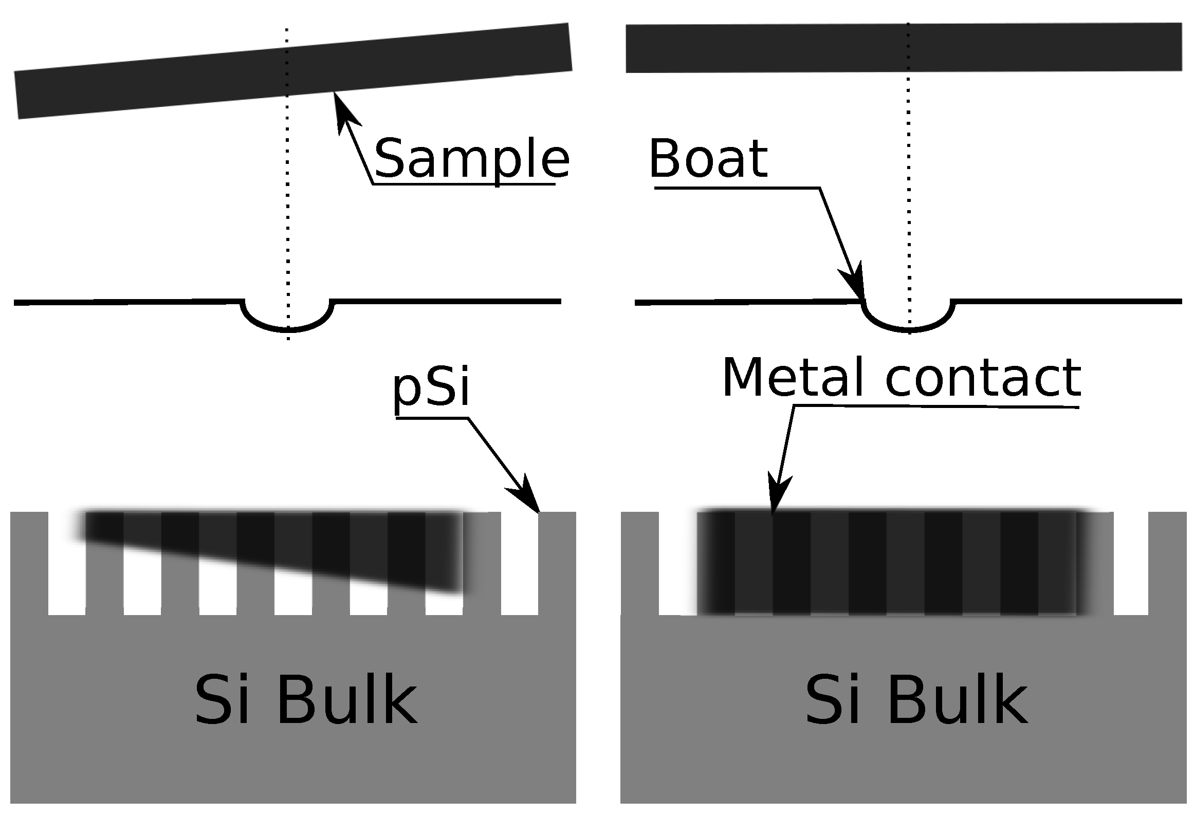
Given the somewhat complex structure of studied PS samples, one may wonder where the measured electrical resistivity and its changes come from. The samples described in this work consist of a thin (∼1.5 μm), porous layer on a thick piece (∼500 μm) of crystal Si. Both electrical contacts lay on top of the oxidized porous layer. We, therefore, propose the equivalent circuit shown in Figure 9. As mentioned above, the upper part of the proposed circuit shows the porous layer (pSi in the figure) separated from the underlying crystalline Si layer (cSi) by a dashed line. The electrical contacts are shown as arrows pointing upwards. Between them, we propose an equivalent of a variable resistance, denoted as R, which represents the resistance of the porous layer in the horizontal direction. The resistance of the pore’s sidewalls is denoted by R, while the resistance of the bulk crystalline Si is denoted by R. The nature of electrical contact between the porous and crystalline Si is controversial, but [46] have concluded that it behaves like a Schottky diode, with the pSi playing the role of the metal part. Therefore, we have incorporated two Schottky diodes at the boundary between the pSi and cSi. These diodes effectively block any DC path between the contacts. If this were not the case, the current would flow through the cSi, and the measured resistance would be on the order of ohms. This was tested by vapor depositing the contacts directly onto the cSi, which, as expected, resulted in non-responsive samples. Another case in which R would dominate was noted when thermal evaporation was performed by placing the porous samples above the evaporation boat with the normal pointing directly into it. This method of evaporation resulted in samples that were non-responsive to the analyte, with the resistance consistently in the order of hundreds of ohms (∼500 ). This can be explained by a metal layer that forms on the walls of the pores (or fills them), all the way from the surface of the pSi to the cSi, which creates direct contact with the cSi. This is shown in Figure 10 on the right.
On the other hand, if the samples were placed at an angle to the normal of the evaporation boat, responsive sensors with a resistance in the range of 10–10 were obtained. This value is confirmed both by the DC measurements during the sensor experiments and by impedance spectroscopy. This can be explained by “pore shadowing”, in which the pore walls cast a “shadow” on the cSi so that only their upper edges are covered with the vaporized metal. This is shown in Figure 10 on the left. In this case, the current must flow either through R and, consequently, be blocked by Schottky contacts between the pSi and cSi, or through R.
For the reasons already given in this section, it can be deduced that the measured variable resistance in the equivalent circuit (Figure 9) corresponds to the horizontal transport through the porous layer (R) between the contacts. The next step in explaining its variability with respect to exposure to the analyte is to investigate the nature of the porous layer, its morphology, and the possible ways that the binding of organic vapors might influence its resistance.
Contact angle measurements confirmed the expected presence of an ODTS layer on the silanized samples. Since the samples treated in this way also lost their resistive response, it can be concluded that the ODTS layer prevents IPA molecules from reaching and interacting with the porous layer. In other words, for this type of sensor to work, a direct interaction between the analyte and the porous layer is obviously required. This can be achieved when the analyte molecules are adsorbed onto the layer, either by physisorption or chemisorption. In the case of IPA (and other organic vapors, see [19]), the resistive response is reversible, whereas the sensors do not recover when exposed to ammonia gas [19]. It can be concluded that physisorption is the dominant process in the former case, while chemical bonding occurs in the latter. In this respect, oxidized PS sensors bear a resemblance to metal oxide semiconductor sensors in that they also require a direct interaction between the analyte and the active layer (e.g., [47,48]).
Various models describing the electrical properties of porous silicon have been described in the literature [45]. However, the most commonly used descriptions are thermally activated hopping and extended-state transport [15,17,45,49,50]. In addition, the electrical conductivity of PS was found to be strongly dependent on the sample porosity (p), showing a decrease in with an increase in p of 40–80% [17,50]. Furthermore, it was suggested that at ∼57% porosity, electron transfer through crystalline PS [17] occurs via an extended state mechanism, while, at higher porosities, hopping conduction begins to contribute. It should be noted here that our thermally oxidized PS has a value of , which is well below the reported values for crystalline conductivity [17,50]. Since the porosity was found to be ∼52% [19], such a low conductivity value is most likely the result of the formed oxide layer isolating the Si crystallites. As a result, the continuous transport of electrons between the crystallites is hindered, and the mechanism changes to electron hopping from one crystallite to another.
The results presented indicate that the degree of oxidation of the porous silicon layer affects its ability to recognize IPA molecules. It is evident from Figure 7 that the response of the samples increases with a higher oxygen-to-silicon ratio (x in SiO). According to [13,46] it was assumed that the adsorbed molecules lower the energy barriers between the crystallites in PS and, thus, increase the conductivity. A similar model was presented by [51] for metal oxide semiconductor sensors and involves a large but finite number of active binding sites for IPA molecules. After binding to the active site, the molecule lowers the barrier by interacting with the oxygen ions in the surface, thus increasing the conductivity.
As more molecules bind to the active sites, the number of free active sites decreases, eventually leading to saturation. This saturation is visible in Figure 7 as the asymptotic behavior of the reaction at higher IPA concentrations, where there is little or no change in the conductivity with the increasing concentration. Similar behavior has been reported in other systems that saturate [51]. The data were fitted with an exponential function, which gave a relatively good fit (R) and clearly shows the saturation effects.
While thermally oxidized samples show a negative response (i.e., R/R < 0) to IPA exposure, samples that were not thermally oxidized or were oxidized at lower temperatures show a positive or almost no response. Oxidized porous silicon sensors show similarities to metal oxide semiconductor sensors, as mentioned earlier. Thus, one way to explain this behavior is to compare the sign of the conductivity change between the two types of sensors. In the literature describing metal oxide semiconductor sensors (e.g., [48]), reactions between the sensor material and the analyte result in an increase in conductivity for n-type semiconductors and a decrease in conductivity for p-type semiconductors. In this work, sensors were fabricated from boron-doped (p-type) silicon wafers. As shown by [52], the dopants remain in the porous silicon layer after etching. Therefore, a porous silicon sensor fabricated from p-doped wafers is expected to exhibit a decrease in conductivity [47]. This is supported by the green curve (N.O.) in Figure 7. In this sense, thermal oxidation, which introduces oxygen atoms into the porous layer, shifts the sensor character from that of a p-type to that of an n-type semiconductor sensor. To further validate this point, future research could be conducted on thermally oxidized porous silicon sensors starting from n-type wafers.
The oxygen atoms introduced into the surface by thermal oxidation of the porous layer could play a threefold role. First, they could passivate the PS, thereby making it immune to further atmospheric oxidation. Second, the presence of oxygen atoms could increase the number of binding sites for polar molecules, thereby enhancing the chemoresistive response of the PS sensors. Third, the back-bound oxide layer on the silicon crystallites could form a barrier that can be easily modulated by adsorbed molecules, further enhancing the response.
5. Conclusions
In conclusion, we find that the chemoresistive response of IPA sensors based on PS can be modulated by varying the oxygen content in the silicon-rich oxide surface of the porous layer. The oxidation of PS could passivate the surface and make the sensor stable in the atmosphere. In addition, the oxygen atoms in the PS layer could enhance the chemoresistive response by acting as active binding sites and an easily lowered barrier between crystallites. Since the experiments presented were conducted at room temperature, the oxidized PS could be used as the basis for an organic vapor sensor without the need for external heating.
Author Contributions
Conceptualization, N.B. and M.I.; formal analysis, N.B. and S.R.; funding acquisition, M.I.; investigation, N.B. and S.R.; methodology, N.B., S.R. and D.R.; project administration, M.I.; resources, D.R. and M.I.; supervision, M.I.; validation, N.B. and S.R.; visualization, N.B. and S.R.; writing—original draft, N.B. and S.R.; writing—review and editing, N.B., S.R., M.R., D.R. and M.I. All authors have read and agreed to the published version of the manuscript.
Funding
This research has been partially supported by SAFU, project KK.01.1.1.01.0001 and by the Croatian Science Foundation under the project (IP–2014–09–7046).
Institutional Review Board Statement
Not applicable.
Informed Consent Statement
Not applicable.
Data Availability Statement
Not applicable.
Acknowledgments
The authors thank Katarina Marušić for goniometric measurements that contributed to the overall quality and completeness of this study.
Conflicts of Interest
The authors declare no conflict of interest.
Abbreviations
The following abbreviations are used in this manuscript:
| EDS | Energy dispersive spectroscopy |
| FTIR | Fourier transform infrared spectroscopy |
| IPA | Isopropanol |
| PS | Porous silicon |
| MEMS | Microelectromechanical systems |
| ODTS | Octadecyltrichlorosilane |
| SCCM | Standard cubic centimeter per minute |
References
- Eranna, G.; Joshi, B.C.; Runthala, D.P.; Gupta, R.P. Oxide Materials for Development of Integrated Gas Sensors—A Comprehensive Review. Crit. Rev. Solid State Mater. Sci. 2004, 29, 111–188. [Google Scholar] [CrossRef]
- Aroutiounian, V. Metal oxide hydrogen, oxygen, and carbon monoxide sensors for hydrogen setups and cells. Int. J. Hydrogen Energy 2007, 32, 1145–1158. [Google Scholar] [CrossRef]
- Yamazoe, N.; Shimanoe, K. New perspectives of gas sensor technology, sens. Sens. Actuators B Chem. 2009, 138, 100–107. [Google Scholar] [CrossRef]
- Seung Eon, M.; Nak-Jin, C.; Hyung-Kun, L.; Jaewoo, L.; Woo Seok, Y. Semiconductor-Type MEMS Gas Sensor for Real-Time Environmental Monitoring Applications, sens. ETRI J. 2013, 35, 617–624. [Google Scholar] [CrossRef]
- Rüffer, D.; Hoehne, F.; Bühler, J. New Digital Metal-Oxide (MOx) Sensor Platform. Sensors 2018, 18, 1052. [Google Scholar] [CrossRef]
- Plecenik, T.; Moško, M.; Haidry, A.; Ďurina, P.; Truchlý, M.; Grančič, B.; Gregor, M.; Roch, T.; Satrapinskyy, L.; Mošková, A.; et al. Fast highly-sensitive room-temperature semiconductor gas sensor based on the nanoscale Pt–TiO2–Pt sandwich, sens. Sens. Actuators B Chem. 2015, 207, 351–361. [Google Scholar] [CrossRef]
- Hyodo, T.; Urata, K.; Kamada, K.; Ueda, T.; Shimizu, Y. Semiconductor-type SnO2-based NO2 sensors operated at room temperature under UV-light irradiation. Sens. Actuators B Chem. 2017, 253, 630–640. [Google Scholar] [CrossRef]
- Jeong, H.; Park, M.; Kwon, S.; Joo, H.; Kwon, H. Highly sensitive and selective room-temperature NO2 gas-sensing characteristics of SnOX-based p-type thin-film transistor. Sens. Actuators B Chem. 2019, 288, 625–633. [Google Scholar] [CrossRef]
- Bilyalov, R.R.; Stalmans, L.; Schirone, L.; Lévy-Clément, C. Use of porous silicon antireflection coating in multicrystalline silicon solar cell processing. IEEE Trans. Electron Devices 1999, 46, 2035–2040. [Google Scholar] [CrossRef]
- Martín-Palma, R.; Manso-Silván, M.; Torres-Costa, V. Biomedical applications of nanostructured porous silicon: A review. J. Nanophotonics 2010, 4, 042502. [Google Scholar] [CrossRef]
- Barillaro, G.; Diligenti, A.; Nannini, A.; Strambini, L.M.; Comini, E.; Sberveglieri, G. Low-concentration NO2 detection with an adsorption porous silicon FET. IEEE Sens. J. 2006, 6, 19–23. [Google Scholar] [CrossRef]
- Ozdemir, S.; Gole, J.L. The potential of porous silicon gas sensors. Curr. Opin. Solid State Mater. Sci. 2008, 11, 92–100. [Google Scholar] [CrossRef]
- Ben-Chorin, M.; Möller, F.; Koch, F. Nonlinear electrical transport in porous silicon. Phys. Rev. B 1994, 49, 2981–2984. [Google Scholar] [CrossRef] [PubMed]
- Ben-Chorin, M.; Kux, A.; Schechter, I. Adsorbate effects on photoluminescence and electrical conductivity of porous silicon. Appl. Phys. Lett. 1994, 64, 481–483. [Google Scholar] [CrossRef]
- Ben-Chorin, M.; Moller, F.; Koch, F.; Schirmacher, W.; Eberhard, M. Hopping transport on a fractal: AC conductivity of porous silicon. Phys. Rev. B 1995, 51, 2199–2213. [Google Scholar] [CrossRef]
- Seals, L.; Gole, J.L.; Tse, L.A.; Hesketh, P.J. Rapid, reversible, sensitive porous silicon gas sensor. J. Appl. Phys. 2002, 91, 2519–2523. [Google Scholar] [CrossRef]
- Aroutiounian, V.M.; Ghulinyan, M.Z. Electrical conductivity mechanisms in porous silicon. Phys. Status Solidi (A) 2003, 197, 462–466. [Google Scholar] [CrossRef]
- Archer, M.; Christophersen, M.; Fauchet, P. Electrical porous silicon chemical sensor for detection of organic solvents. Sens. Actuators B Chem. 2005, 106, 347–357. [Google Scholar] [CrossRef]
- Baran, N.; Gebavi, H.; Mikac, L.; Ristić, D.; Gotić, M.; Syed, K.; Ivanda, M. Sensing Properties of Oxidized Nanostructured Silicon Surface on Vaporized Molecules. Sensors 2019, 19, 119. [Google Scholar] [CrossRef]
- Lewis, S.E.; DeBoer, J.R.; Gole, J.L.; Hesketh, P.J. Sensitive, selective, and analytical improvements to a porous silicon gas sensor. Sens. Actuators B Chem. 2005, 110, 54–65. [Google Scholar] [CrossRef]
- Aroutiounian, V.; Arakelyan, V.; Galstyan, V.; Martirosyan, K.; Soukiassian, P. Hydrogen Sensor Made of Porous Silicon and Covered by TiO2 or ZnO Thin Film. IEEE Sens. J. 2009, 9, 9–12. [Google Scholar] [CrossRef]
- Korotcenkov, G.; Rusu, E. How to Improve the Performance of Porous Silicon-Based Gas and Vapor Sensors? Approaches and Achievements. Phys. Status Solidi (A) 2019, 216, 1900348. [Google Scholar] [CrossRef]
- Rigakis, N.; Hilliard, J.; Abu Hassan, L.; Hetrick, J.M.; Andsager, D.; Nayfeh, M.H. Effect of oxidation treatments on photoluminescence excitation of porous silicon. J. Appl. Phys. 1997, 81, 440–444. [Google Scholar] [CrossRef]
- Bazrafkan, I.; Dariani, R.S. Electrical behavior of free-standing porous silicon layers. Phys. B Condens. Matter 2009, 404, 1638–1642. [Google Scholar] [CrossRef]
- Salonen, J.; Lehto, V.P.; Laine, E. Thermal oxidation of free-standing porous silicon films. Appl. Phys. Lett. 1997, 70, 637–639. [Google Scholar] [CrossRef]
- Salonen, J.; Laine, E.; Niinistö, L. Thermal carbonization of porous silicon surface by acetylene. J. Appl. Phys. 2002, 91, 456. [Google Scholar] [CrossRef]
- Ibraimov, M.K.; Sagidolda, Y.; Rumyantsev, S.L.; Zhanabaev, Z.Z.; Shur, M.S. Selective Gas Sensor Using Porous Silicon. Sens. Lett. 2016, 14, 588–591. [Google Scholar] [CrossRef]
- Brugnone, F.; Perbellini, L.; Apostoli, P.; Bellomi, M.; Caretta, D. Isopropanol exposure: Environmental and biological monitoring in a printing works. Occup. Environ. Med. 1983, 40, 160–168. [Google Scholar] [CrossRef]
- Chien, P.J.; Suzuki, T.; Ye, M.; Toma, K.; Arakawa, T.; Iwasaki, Y.; Mitsubayashi, K. Ultra-Sensitive Isopropanol Biochemical Gas Sensor (Bio-Sniffer) for Monitoring of Human Volatiles. Sensors 2020, 20, 6827. [Google Scholar] [CrossRef]
- Peng, L.; Zhai, J.; Wang, D.; Zhang, Y.; Wang, P.; Zhao, Q.; Xie, T. Size- and photoelectric characteristics-dependent formaldehyde sensitivity of ZnO irradiated with UV light. Sens. Actuators B Chem. 2010, 148, 66–73. [Google Scholar] [CrossRef]
- Vallant, T.; Brunner, H.; Mayer, U.; Hoffmann, H.; Leitner, T.; Resch, R.; Friedbacher, G. Formation of Self-Assembled Octadecylsiloxane Monolayers on Mica and Silicon Surfaces Studied by Atomic Force Microscopy and Infrared Spectroscopy. J. Phys. Chem. B 1998, 102, 7190–7197. [Google Scholar] [CrossRef]
- Resch, R.; Grasserbauer, M.; Friedbacher, G.; Vallant, T.; Brunner, H.; Mayer, U.; Hoffmann, H. In situ and ex situ AFM investigation of the formation of octadecylsiloxane monolayers. Appl. Surf. Sci. 1999, 140, 168–175. [Google Scholar] [CrossRef]
- Leitner, T.; Friedbacher, G.; Vallant, T.; Brunner, H.; Mayer, U.; Hoffmann, H. Investigations of the Growth of Self-Assembled OctadecylsiloxaneMonolayers with Atomic Force Microscopy. Microchim. Acta 2000, 133, 331–336. [Google Scholar] [CrossRef]
- Yon, J.J.; Barla, K.; Herino, R.; Bomchil, G. The kinetics and mechanism of oxide layer formation from porous silicon formed on p-Si substrates. J. Appl. Phys. 1987, 62, 1042–1048. [Google Scholar] [CrossRef]
- Pap, A.E.; Kordás, K.; George, T.F.; Leppävuori, S. Thermal Oxidation of Porous Silicon: Study on Reaction Kinetics. J. Phys. Chem. B 2004, 108, 12744–12747. [Google Scholar] [CrossRef]
- Lucovsky, G.; Yang, J.; Chao, S.S.; Tyler, J.E.; Czubatyj, W. Oxygen-bonding environments in glow-discharge-deposited amorphous silicon-hydrogen alloy films. Phys. Rev. B 1983, 28, 3225–3233. [Google Scholar] [CrossRef]
- Gupta, P.; Dillon, A.C.; Bracker, A.S.; George, S.M. FTIR studies of H2O and D2O decomposition on porous silicon surfaces. Surf. Sci. 1991, 245, 360–372. [Google Scholar] [CrossRef]
- Gupta, P.; Colvin, V.L.; George, S.M. Hydrogen desorption kinetics from monohydride and dihydride species on silicon surfaces. Phys. Rev. B 1988, 37, 8234–8243. [Google Scholar] [CrossRef]
- Borghesi, A.; Guizzetti, G.; Sassella, A.; Bisi, O.; Pavesi, L. Induction-model analysis of Si-H stretching mode in porous silicon. Solid State Commun. 1994, 89, 615–618. [Google Scholar] [CrossRef]
- Ogata, Y.; Niki, H.; Sakka, T.; Iwasaki, M. Oxidation of Porous Silicon under Water Vapor Environment. J. Electrochem. Soc. 1995, 142, 1595. [Google Scholar] [CrossRef]
- Lenshin, A.S.; Kashkarov, V.M.; Seredin, P.V.; Spivak, Y.M.; Moshnikov, V.A. XANES and IR spectroscopy study of the electronic structure and chemical composition of porous silicon on n- and p-type substrates. Semiconductors 2011, 45, 1183. [Google Scholar] [CrossRef]
- Ogata, Y.; Niki, H.; Sakka, T.; Iwasaki, M. Hydrogen in Porous Silicon: Vibrational Analysis of SiH x Species. J. Electrochem. Soc. 1995, 142, 195. [Google Scholar] [CrossRef]
- Richter, H.; Wang, Z.P.; Ley, L. The one phonon Raman spectrum in microcrystalline silicon. Solid State Commun. 1981, 39, 625–629. [Google Scholar] [CrossRef]
- Campbell, I.H.; Fauchet, P.M. The effects of microcrystal size and shape on the one phonon Raman spectra of crystalline semiconductors. Solid State Commun. 1986, 58, 739–741. [Google Scholar] [CrossRef]
- Canham, L. (Ed.) Handbook of Porous Silicon; Springer International Publishing: Berlin/Heidelberg, Germany, 2014. [Google Scholar] [CrossRef]
- Schechter, I.; Ben-Chorin, M.; Kux, A. Gas Sensing Properties of Porous Silicon. Anal. Chem. 1995, 67, 3727–3732. [Google Scholar] [CrossRef]
- Nazemi, H.; Joseph, A.; Park, J.; Emadi, A. Advanced Micro- and Nano-Gas Sensor Technology: A Review. Sensors 2019, 19, 1285. [Google Scholar] [CrossRef]
- Barsan, N.; Weimar, U. Understanding the fundamental principles of metal oxide based gas sensors; the example of CO sensing with SnO2 sensors in the presence of humidity. J. Phys. Condens. Matter 2003, 15, R813–R839. [Google Scholar] [CrossRef]
- Balberg, I. Transport in porous silicon: The pea-pod model. Philos. Mag. B 2000, 80, 691–703. [Google Scholar] [CrossRef]
- Korotcenkov, G. (Ed.) Porous Silicon: From Formation to Applications: Optoelectronics, Microelectronics, and Energy Technology Applications, Volume Three; CRC Press: Boca Raton, FL, USA, 2016. [Google Scholar] [CrossRef]
- Srivastava, R.K.; Lal, P.; Dwivedi, R.; Srivastava, S.K. Sensing mechanism in tin oxide-based thick-film gas sensors. Sens. Actuators B Chem. 1994, 21, 213–218. [Google Scholar] [CrossRef]
- Bisi, O.; Ossicini, S.; Pavesi, L. Porous silicon: A quantum sponge structure for silicon based optoelectronics. Surf. Sci. Rep. 2000, 38, 1–126. [Google Scholar] [CrossRef]
Figure 1.
Schematic view of the measurement setup.

Figure 2.
SEM images of samples oxidized at different temperatures given in the upper left and an image of the cross-section of a sample (bottom right).
Figure 2.
SEM images of samples oxidized at different temperatures given in the upper left and an image of the cross-section of a sample (bottom right).
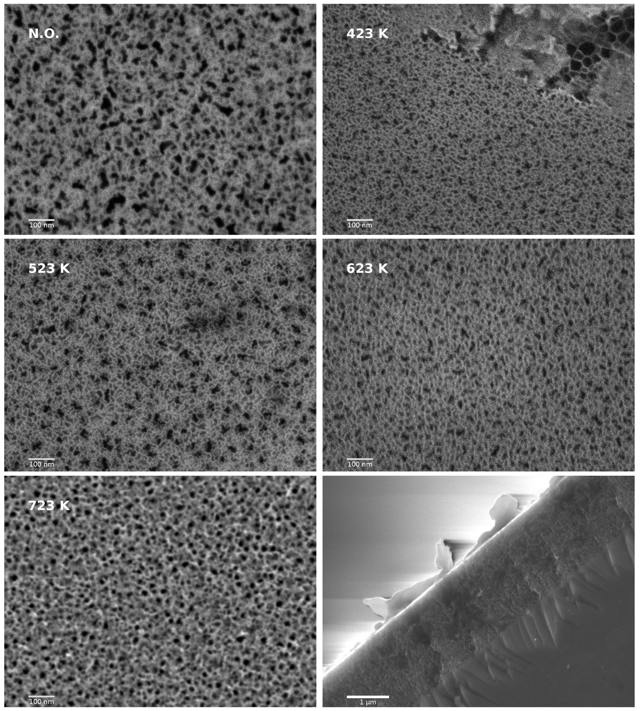
Figure 3.
Ratio of oxygen to silicon (x in SiO) in the surface of the samples, as measured using EDS vs. oxidation temperature.
Figure 3.
Ratio of oxygen to silicon (x in SiO) in the surface of the samples, as measured using EDS vs. oxidation temperature.
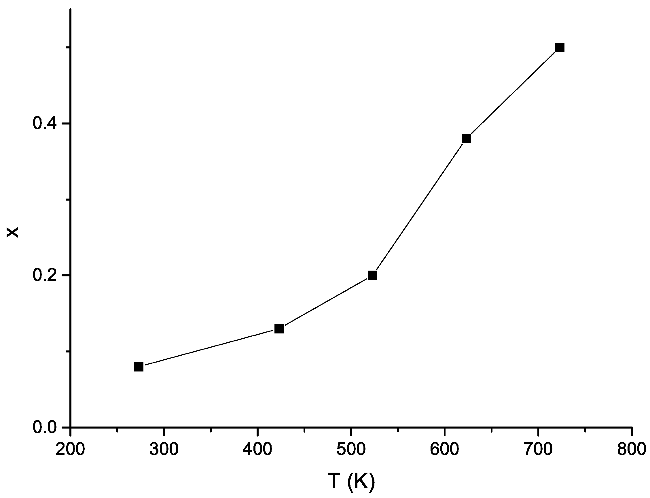
Figure 4.
Average FTIR spectrum of thermally oxidized samples (solid black line) and a spectrum of unoxidized sample (dashed blue line).
Figure 4.
Average FTIR spectrum of thermally oxidized samples (solid black line) and a spectrum of unoxidized sample (dashed blue line).
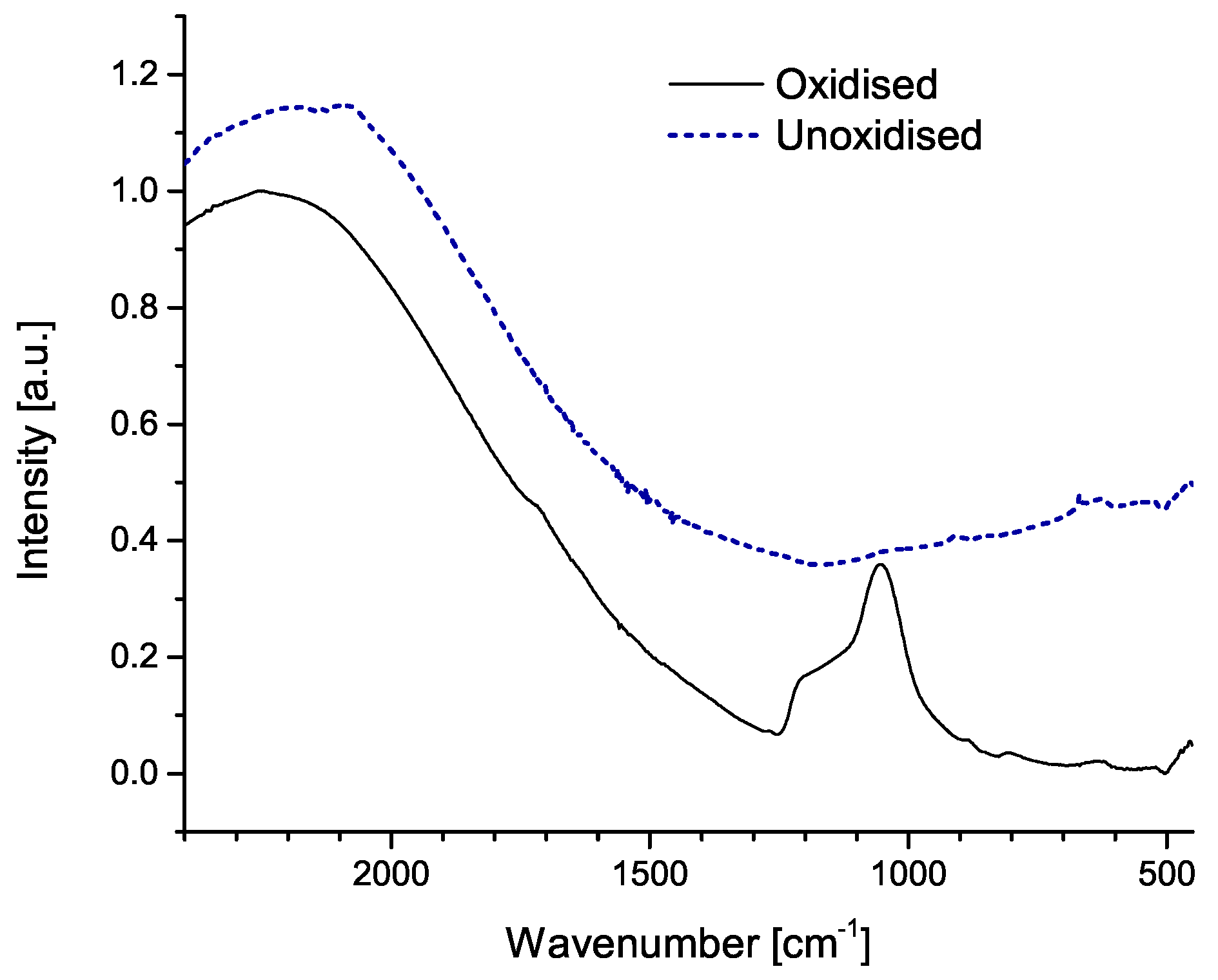
Figure 5.
Raman spectra of samples oxidized at different temperatures. Legend shows oxidation temperature in Kelvin, while N.O. stands for samples that were not thermally oxidized.
Figure 5.
Raman spectra of samples oxidized at different temperatures. Legend shows oxidation temperature in Kelvin, while N.O. stands for samples that were not thermally oxidized.
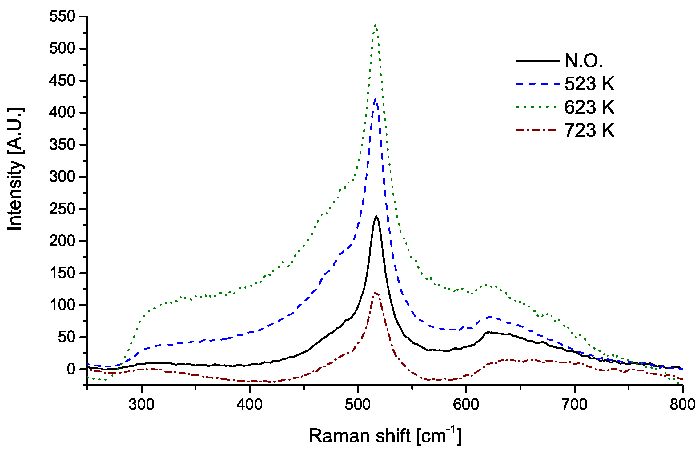
Figure 6.
(a) Conductivity spectra at different temperatures and (b) Arrhenius plot of DC conductivity for a PS sample thermally oxidized at 250 °C. No difference was observed between heating and cooling runs. The error bars in (b) are at most in the order of magnitude of the symbol size.
Figure 6.
(a) Conductivity spectra at different temperatures and (b) Arrhenius plot of DC conductivity for a PS sample thermally oxidized at 250 °C. No difference was observed between heating and cooling runs. The error bars in (b) are at most in the order of magnitude of the symbol size.
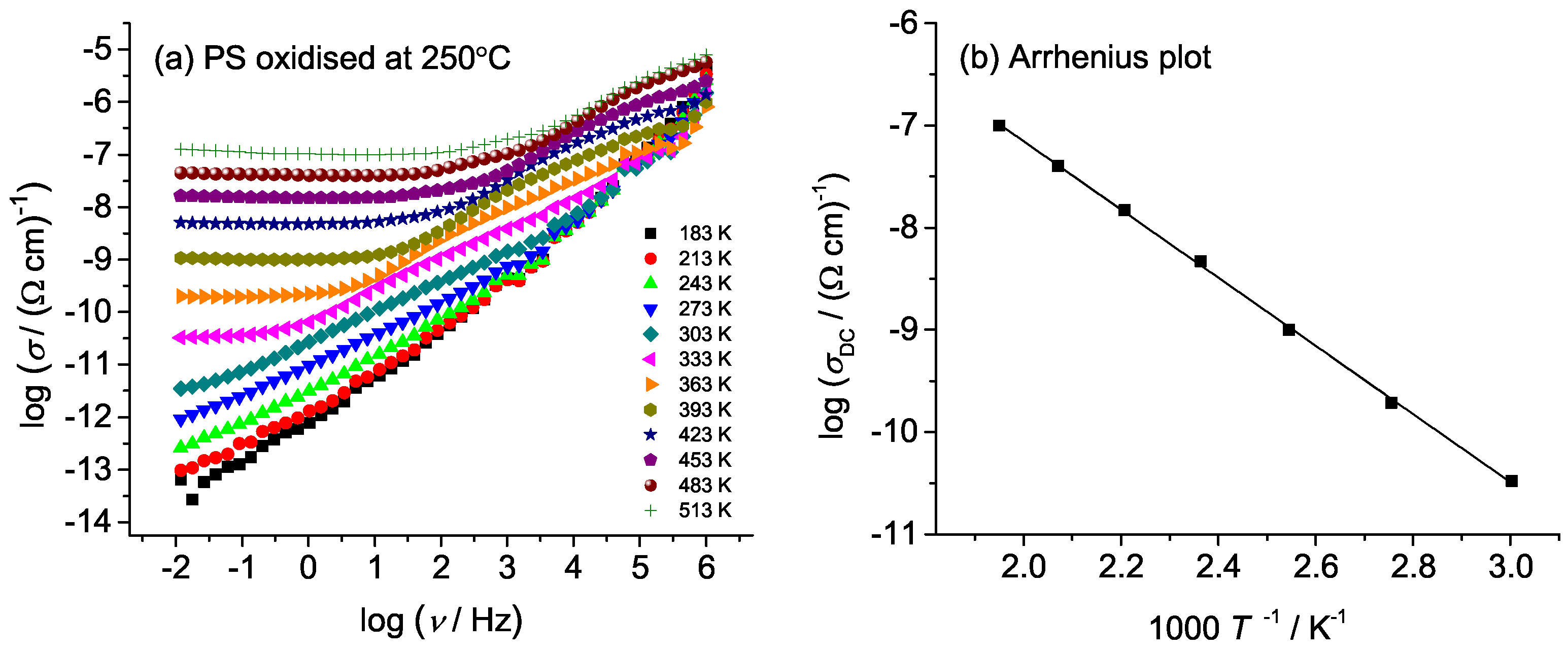
Figure 7.
Sensor response as a function of IPA concentration. Legend shows thermal oxidation temperature of the samples. Data were fitted with exponential function. The error bars are at most in the order of the symbol size.
Figure 7.
Sensor response as a function of IPA concentration. Legend shows thermal oxidation temperature of the samples. Data were fitted with exponential function. The error bars are at most in the order of the symbol size.
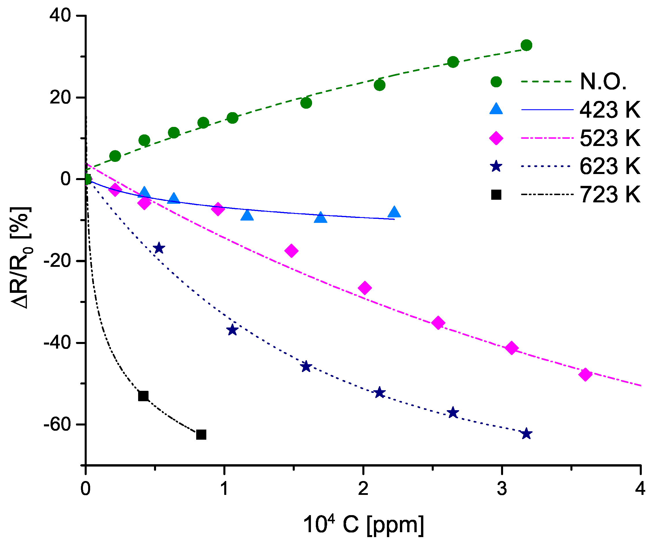
Figure 8.
Contact between water and (left) oxidized PS surface and (right) oxidized PS surface treated with ODTS.
Figure 8.
Contact between water and (left) oxidized PS surface and (right) oxidized PS surface treated with ODTS.

Figure 9.
Proposed equivalent circuit of the sensors presented in this work. The resistance between the porous Si layer (pSi) and the crystal layer (cSi) is shown as R. The resistance of the crystal layer is shown as R, while R is the proposed variable resistance between the contacts shown with arrows. The dashed line marks the boundary between the porous and crystalline layers. See Section 4 for details.

Figure 10.
(Left) The sample is placed obliquely to the normal of the evaporation boat. (Right) The sample is placed at a normal with respect to the boat. The normal is shown as a dashed line. The resulting contact geometries are shown in the lower figures. Although both figures have similar features, the annotations have been placed on only one side of each for clarity. For details, see Section 4.

Table 1.
Estimated sensitivities of sensors oxidized at different temperatures (N.O. stands for not oxidized) as calculated by approximating a linear response below 1.5 × 10 ppm.
Table 1.
Estimated sensitivities of sensors oxidized at different temperatures (N.O. stands for not oxidized) as calculated by approximating a linear response below 1.5 × 10 ppm.
| T [K] | S × 10 [%/ppm] |
|---|---|
| N.O | 1.6 |
| 423 | −0.6 |
| 523 | −1.1 |
| 623 | −2.9 |
| 723 | −7.5 |
Publisher’s Note: MDPI stays neutral with regard to jurisdictional claims in published maps and institutional affiliations. |
© 2022 by the authors. Licensee MDPI, Basel, Switzerland. This article is an open access article distributed under the terms and conditions of the Creative Commons Attribution (CC BY) license (https://creativecommons.org/licenses/by/4.0/).
Share and Cite
MDPI and ACS Style
Baran, N.; Renka, S.; Raić, M.; Ristić, D.; Ivanda, M. Effects of Thermal Oxidation on Sensing Properties of Porous Silicon. Chemosensors 2022, 10, 349. https://doi.org/10.3390/chemosensors10090349
AMA Style
Baran N, Renka S, Raić M, Ristić D, Ivanda M. Effects of Thermal Oxidation on Sensing Properties of Porous Silicon. Chemosensors. 2022; 10(9):349. https://doi.org/10.3390/chemosensors10090349
Chicago/Turabian StyleBaran, Nikola, Sanja Renka, Matea Raić, Davor Ristić, and Mile Ivanda. 2022. "Effects of Thermal Oxidation on Sensing Properties of Porous Silicon" Chemosensors 10, no. 9: 349. https://doi.org/10.3390/chemosensors10090349
Note that from the first issue of 2016, this journal uses article numbers instead of page numbers. See further details here.