Communication

Investigation of the Atomic Layer Deposition of the Titanium Dioxide (TiO2) Film as pH Sensor Using a Switched Capacitor Amplifier

by
Mozhdeh Nematzadeh
1,
Ola Nilsen
2,*,
Philipp Dominik Häfliger
1 and
Veronica Anne-Line Kathrine Killi
2
1
Department of Informatics, University of Oslo, Problemveien 7, 0315 Oslo, Norway
2
Centre for Materials Science and Nanotechnology (SMN), Department of Chemistry, University of Oslo, Problemveien 7, 0315 Oslo, Norway
*
Author to whom correspondence should be addressed.
Chemosensors 2022, 10(7), 274; https://doi.org/10.3390/chemosensors10070274
Submission received: 7 June 2022 / Revised: 1 July 2022 / Accepted: 6 July 2022 / Published: 12 July 2022
(This article belongs to the Section Materials for Chemical Sensing)

Abstract

:
The electrical and chemical properties of the titanium dioxide (TiO2) coated spirals grown by the atomic layer deposition (ALD) technique in two different temperatures of 150 °C and 300 °C are studied. The thickness of the TiO2 layers studied are 20, 40, and 80 nm. A switched capacitor amplifier is used to investigate the pH response and the capacitance of the samples. It is found that the performance of the TiO2 samples depends on either the thickness or the deposition temperature due to the differences in the physical properties of the oxide layer such as surface roughness and film density. The high temperature samples are more crystalline, whereas the low temperature samples are more amorphous. Since there is a low pass filter effect in the electrolyte–sample interface, the TiO2 coated samples show the better response to the pH change for the high temperature samples as the sensor surface area for binding the hydrogen ions is larger and the charge transfer resistance is smaller. Furthermore, more roughness on the surface can be obtained by increasing the thickness, which reduces the charge transfer resistance. In this study, the 80 nm sample deposited at 300 °C gives the best pH response of 40 mV/pH.

Graphical Abstract

1. Introduction

In biomedical applications, such as high resolution chemical sensors, ion-sensitive field effect transistors (ISFETs) are a popular choice. They were first developed by P. Bergveld in 1970 [1] and provide a fast response, are compatible with integrated circuit (IC) production processes, and have a compact structure. ISFETs are common metal–oxide–semiconductor (MOS) transistors where the gate of the transistor is floating and is controlled by a reference electrode in an electrolyte solution through the capacitive coupling between the passivation layer and the gate oxide. So far, different types of materials have been used as the passivation layer in the ISFET such as titanium dioxide (TiO2) [2], silicon nitride (Si3N4) [3], aluminum oxide (Al2O3) [4], Si nanowire/SiO2/Al2O3 [5], tantalum pentoxide (Ta2O5) [6], tin oxide (SnO2) [7], and hafnium dioxide (HfO2) [8]. TiO2 is known as a good candidate for the pH sensitive layer due to the high dielectric constant, high stability, and high sensitivity. TiO2 has been used in a variety of applications such as extended-gate ISFETs (EGFET) [9], photocatalytic probing of DNA [10], capture of circulating tumor cells on aptamer modified TiO2 [11], and gas sensor [12].
The pH sensitivity can be explained as the ion exchange in a surface layer containing hydroxide groups [13]. Higher conductivity results in better sensing performance of a pH sensor since the system responds faster to the pH change. The physical properties of the samples depend on the deposition temperature and the thickness. The high temperature samples (300 °C) are more crystalline and have a greater surface area, whereas the low temperature samples (150 °C) are amorphous and have diminished surface roughness. Moreover, the surface roughness and the surface area increase with increasing the thickness. The electrolyte–sample–amplifier interface forms a band-pass filter where the filter response can be improved by manipulating the low cutoff frequency and high cutoff frequency to have a higher gain in the pass band. There are several methods that are often used to prepare the TiO2 film such as the atomic layer deposition (ALD), sputtering [14], metal–organic chemical vapor deposition (MOCVD) [15], and the sol–gel technique [16]. ALD has been widely used for growing uniform thin films with precise thickness as the thickness is controlled on an atomic scale. The compact layer of TiO2 deposited by ALD can be prepared at low temperature (<300 °C). Thus, low fabrication cost and pinhole-free thin film, which is compatible with a large range of substrates, can be achieved [17].
In this paper, the characteristics of the TiO2 film deposited by the ALD technique with different thickness and deposition temperatures are studied. In Section 2, the sample preparation is explained and the electrical model of the sample tested in an aqueous solution and the system used for measuring the capacitance and pH sensitivity of the samples are presented. Measurement results are discussed in Section 3 and finally the paper is concluded in Section 4.

2. Materials and Methods

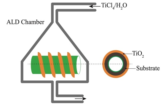
2.1. Sample Preparation

The TiO2 films are deposited in a F-120 Sat reactor (ASM Microchemistry) using TiCl4 (Sigma Aldrich, St. Louis, MO, USA, 99.9%) and H2O (type II) as precursors. Both are kept at ambient conditions outside the reactor. Nitrogen purging gas is supplied from a Schmidlin Sirocco5 generator producing 99.9995% (N2 + Ar) and maintained at a 500 cm3min−1 total flow rate. Reactor operating pressure is maintained at approximately 6 mbar throughout the depositions [18].
The films are deposited at 150 °C and 300 °C, using a pulsing scheme of 1 s TiCl4, 2 s purge, 1 s H2O and 2 s purge. All verified to be within the ALD regime for the current reactor. The film thickness is controlled by choice of number of deposition cycles and the area of the samples is about 3 cm2. The surface roughness of the TiO2 coated samples is studied by using atomic force microscopy (AFM). Topography analysis is performed using a Park Systems XE-70 AFM equipped with a standard NHCR tip. Data are analyzed using the gwyddion 2.60 spm visualization software [19]. We can see from AFM images of the 80 nm samples that the high temperature deposition creates a rougher surface (Figure 1). The projected area is considered to be 4 μ m 2 . Note that the 300 °C sample is measured on a scale of 0 to 35 nm and the 150 °C sample is measured on a scale of 0 to 5 nm. The RMS value of the surface roughness is obtained as 5 nm and 0.5 nm for the deposition temperature of 300 °C and 150 °C, respectively. The surface area is measured as 4.255 μ m 2 and 4.005 μ m 2 for the 300 °C and 150 °C sample, respectively. This is according to prior reports on deposition of TiO2 by the same process where a low deposition temperature results in dominating amorphous TiO2 with a low surface roughness. Crystallites of anatase are formed for higher deposition temperatures leading to an increase in surface roughness [20,21].

2.2. Electrical Model of Electrode–Electrolyte–Sample Interface

A model for the ALD sample measured in an aqueous solution is proposed in Figure 2. In this model, C p represents the reference/counter electrode polarization [22], R s o l is the resistance of the electrolyte, R c t is the charge transfer resistance, C dl is the double layer capacitance, and R a and C a are the leaky resistance and capacitance of the sample, respectively. It should be noted that that R c t and C d l relate to the surface structure. When the solid surface comes in contact with the liquid, the potential Ψ 0 is established on the surface depending on the pH value and the ionic strength of the medium. This means that Ψ 0 is the pH-dependent parameter.

2.3. Measurement Setup

Figure 3 shows the system used to characterize the electrical and chemical properties of the TiO2 coated spirals. The proposed circuit is a switched capacitor amplifier where the gain is given by the ratio between the input capacitor (i.e., the equivalent capacitance between counter/reference electrode (CE/RE) and negative input of the amplifier) and the feedback capacitor C f . At t = 0 s, the switch S1 resets the amplifier’s output to zero. For measuring the sample’s capacitance C a , an AC signal is applied through the platinum electrode (Pt) to the aqueous solution as the CE. In this case, the switch S1 turns on to short the capacitor C i so that the input capacitance becomes the capacitor C a and the gain becomes equal to the capacitor C a divided by the capacitor C f . However, for the chemical measurement the switch S2 turns off and the equivalent input capacitance becomes the capacitor C i where its value is chosen to be a few orders of magnitude smaller than the capacitor C a . In this case, the gain is defined as the capacitor C i divided by the capacitor C f and remains constant for different samples.
G a i n = C i / C f , if the switch S 2   is OFF . C a / C f , if the switch S 2   is ON .
Thus, we can measure the surface charge change using (2).
Δ Q = Δ V in . C i = Δ V out / G a i n
Mainly, there are two reasons for having the capacitor C i in the chemical measurement: (a) measuring the sensitivity without knowing the exact value of the capacitance of the sample and (b) reducing the amount of drift at the amplifier’s output. Since the spiral samples have a high capacitance of 1–30 μ F, the electrode polarization and the distance between the Pt electrode and the sample may influence the gain and the measured capacitance as well. It is therefore effective to make the gain independent of the capacitor C a . Variations on the surface potential of Ψ 0 can cause the output voltage to drift toward ±VCC. A significant error can be introduced to the high gain amplifier, however. Placing the capacitor C i between the sample and the amplifier can negate the output drift with the appropriate capacitive value. Note that for the chemical measurement, the Pt electrode is replaced by the silver–silver chloride (Ag–AgCl) electrode as the RE to make the solution potential stable.

3. Results and Discussion

3.1. Capacitance Measurement

The capacitance of the sample is obtained by measuring the amplifier gain at the frequency of 10 mHz and then using (1) when the switch S2 turns on. When the capacitor C f is at 0.1 μ F, a 10 mV peak-to-peak square waveform signal is applied to the pH 7 buffer solution through the Pt electrode and the capacitor C f is chosen to be 0.1 μ F. The gain magnitude over frequency is plotted for the samples of different thickness in different temperatures of 300 °C and 150 °C in Figure 4a,b, respectively.
As shown, when the frequency is further reduced (<10 mHz), the gain becomes more stable and the capacitance value is more accurate. The measured value of the capacitance of the samples over thickness is depicted in Figure 5. Using (3), the sample capacitance can be calculated.
C a = ϵ 0 ϵ r A / t ox ( eff )
where ϵ 0 is the permittivity of free space, ϵ r is the relative permittivity of the TiO2 film, A is the area of the spiral sample, and t ox ( eff ) is the effective thickness of the sample. Since the sample surface is not uniform, the effective thickness should be considered in computing the capacitance by (3). It can be seen that the absolute value of the capacitance from the 300 °C sample is smaller than the low temperature sample for the same thickness of oxide. One explanation is that as the low temperature sample is more amorphous, t ox ( eff ) is lower than the high temperature sample even though the area of the high temperature sample is greater as depicted in Figure 6. This is also proven by the AFM data as the RMS value of the surface roughness for the low temperature sample is 10 times smaller than the high temperature sample.

3.2. Series Resistance Measurement

The resistor R sol + R ct is the series resistance with sample. In order to measure it, the switch S2 turns off and a square waveform with amplitude of 100 mV is applied to the aqueous solution. Since the frequency to be measured is increased up to 100 kHz, the buffer solution is not suitable in this case due to the high capacitance of the solution as the signal generator is not able to drive it. Thus, the buffer solution is replaced by tap water. The input capacitance to the system is identical and equal to the capacitor C i for different samples and the capacitors C i and C f have the same value of 0.1 μ F. The output voltage over frequency for the sample of 20, 40, and 80 nm deposited in two different temperatures is plotted in Figure 7. It can be seen that the high temperature sample with crystalline structure shows higher bandwidth or lower series resistance than the low temperature sample. The difference in the resistor R s is possibly due to the different value of the resistor R ct rather than R sol . Then, the R s value is calculated using (4). The R s versus film thickness is drawn in Figure 8.
R s = 1 / 2 π C i f 3 dB

3.3. Drift Measurement

For this purpose, the switch S2 turns off and the potential of the pH 7 buffer solution is kept at the fixed value through the Ag–AgCl electrode. From (1), the gain is unity and the capacitance values are set to 0.1 μ F. Any variation at the output voltage can be explained as the drift. The drift of the samples versus thickness is sketched in Figure 9. As the film thickness increases, the drift values from the 150 °C and 300 °C samples converge and cross over at 70 nm. Prior to the crossover point the amorphous sample, the sample at 150 °C had the greater drift value. Afterward, it had the smaller value by 0.02 mV/s. Referring to the amplifier’s datasheet (i.e. AD8065 [23]), the amplifier needs 1 pA as input bias current. However, leakage currents that are innate to PCB materials and environmental contaminates such as skin oils can be higher than the bias current. Thus, the drift value measured includes the amplifier’s leakage as well, which is supposed to be the same for different samples.

3.4. The pH Response Measurement

The chemical measurement is carried out in the buffer solution where the pH level is increased from pH 4 → pH 7 by dropwise addition of sodium hydroxide (NaOH) 0.2 M. The pH of the solution is measured by Testo 206 Series pH1/Temperature measurement instrument in each step. In order to measure the output voltage, a Keithley 2636 sourcemeter unit is used. A magnetic stirrer is utilized to quickly and consistently mix the solution and rapidly reach a stable pH level when the base is added. In this experiment, the input capacitance and the feedback capacitance values do not change, and the gain of one is expected from the amplifier circuit. Each sample had a small and controlled pH change of 0.2 to 0.4 to obtain reliable response values. The output voltage was then measured before adding the samples together. The output voltage versus pH value is drawn in Figure 10 for different samples where the slope of these plots shows the pH response. Figure 11 shows how the output voltage of each TiO2 sample changes over time, normalized for pH of 1. The overshoot in the step response of Figure 11d,f are due to the adding the solution close to the sensor.
The maximum response of the system is limited by the combination of a low-pass characteristics dominated by the series resistance R s and the TiO2 capacitance and a high-pass characteristics dominated by the size of the total capacitance on the input node and parasitic leakage at the internal nodes of the front-end ( R l ) and/or through the sample parallel resistance R a . The low-pass and high pass filter seem to overlap in their respective cutoff/rolloff regions. They both limit the maximum response as the low-pass cutoff frequency ( f clp ) is lower than high-pass cutoff frequency ( f chp ). Increasing their overlap will increase the maximum response up to a point where the f clp becomes higher than the f chp . Then, the response will have reached its absolute maximum. The low-pass and high-pass characteristics are sketched in Figure 12 where the corresponding cutoff frequency can be obtained using (5) and (6).
f clp = 1 R s ( C a C i C a + C i )
f chp = 1 R l ( C a + C i )
Note that the contribution of the sample resistance R a is neglected in above equations and R l represents the leakage, the value of which increases by increasing the thickness. The crossing point of the low-pass filter (LPF) and high-pass filter (HPF) forming a band-pass filter is shown in Figure 12a where the response is less than the maximum value. Increasing the ruggedness with higher deposition temperature will increase LPF and HPF overlap and thus the response as shown in Figure 12b. Maximum is reached as the cutoff frequencies cross ( f chp < f clp ). Increasing thickness also increases the response until the LPF and HPF overlap completely as shown in Figure 12c. Then, it will remain constant until the sample TiO2 capacitance becomes too small and the LPF DC gain will decline once the TiO2 capacitor is no longer significantly bigger than the internal capacitors of the front-end and the parasitics as shown in Figure 12d. The dashed line shows the DC gain before the further increase of the thickness. Note that increasing temperature increases the overlap more effectively as the HPF cutoff does remain stable.
The pH response as function of thickness is shown in Figure 13 for the samples in two different temperatures. As seen, the high temperature samples show better response to pH, which is in good agreement with the measured lower series resistance for them. It is also shown that by increasing the thickness, the pH response improves due to the more roughness on the surface as expected. Finally, in Table 1, the properties of the ALD deposited TiO2 samples are summarized.

4. Conclusions

In this work, the properties of the TiO2 coated spirals grown by ALD technique are studied using a capacitive feedback amplifier. The effect of the thickness of the TiO2 and the deposition temperature on the pH response are discussed. The electrolyte–sample–amplifier interface shows a band-pass filter behavior as the low cutoff frequency and high cutoff frequency can be modulated by the surface structure of the sample. Maximum response is achieved for the higher bandwidth systems. Increasing the temperature increases the response more effectively as the low cutoff frequency remains stable and the high cutoff frequency increases. Increasing thickness for increasing the response is useful until the sample capacitance becomes too small compared to the input capacitance and parasitic capacitance of the front-end and the DC gain will decline.

Author Contributions

The sensors were fabricated by V.A.-L.K.K. and O.N. The AFM images were taken by V.A.-L.K.K. The test and measurement were conducted by M.N., P.D.H. and O.N. contributed in discussions regarding this measurement technique and modeling of the sample–electrolyte interface and the results. All authors have read and agreed to the published version of the manuscript.

Funding

This research received no external funding.

Institutional Review Board Statement

Not applicable.

Informed Consent Statement

Not applicable.

Data Availability Statement

Not applicable.

Acknowledgments

This work has been supported by the Norwegian Centre of Excellence ’Hybrid Technology Hub’ (HTH) (262613), the Norwegian Research Council project ’PhotoSense’, and Baldur Coatings AS.

Conflicts of Interest

The authors declare no competing interests or other interests that might be perceived to influence the results and discussion reported in this paper.

Abbreviations

The following abbreviations are used in this manuscript:
ALDAtomic Layer Deposition
ISFETIon-Sensitive Field Effect Transistors
REReference Electrode
CECounter Electrode
LPFLow Pass Filter
HPFHigh Pass Filter

References

  1. Bergveld, P. Thirty years of ISFETOLOGY: What happened in the past 30 years and what may happen in the next 30 years. Sens. Actuat. Chem. 2003, 88, 1–20. [Google Scholar] [CrossRef] [Green Version]
  2. Liao, Y.H.; Chou, J.C. Preparation and characterization of the titanium dioxide thin films used for pH electrode and procaine drug sensor by sol–gel method. Mater. Chem. Phys. 2009, 114, 542–548. [Google Scholar] [CrossRef]
  3. Yin, L.T.; Chou, J.C.; Chung, W.Y.; Sun, T.P.; Hsiung, S.K. Characteristics of silicon nitride after O2 plasma surface treatment for pH-ISFET applications. IEEE Trans. Biomed. Eng. 2001, 48, 340–344. [Google Scholar] [CrossRef] [PubMed]
  4. Jakobson, C.; Dinnar, U.; Feinsod, M.; Nemirovsky, Y. Ion-sensitive field-effect transistors in standard CMOS fabricated by post processing. IEEE Sens. J. 2002, 2, 279–287. [Google Scholar] [CrossRef]
  5. Knopfmacher, O.; Tarasov, A.; Fu, W.; Wipf, M.; Niesen, B.; Calame, M.; Schönenberger, C. Nernst Limit in Dual-Gated Si-Nanowire FET Sensors. Nano Lett. 2010, 10, 2268–2274. [Google Scholar] [CrossRef]
  6. Bahari, N.; Zain, A.M.; Abdullah, A.Z.; Sheng, D.B.C.; Othman, M. Study on pH sensing properties of RF magnetron sputtered tantalum pentoxide (Ta2O5) thin film. In Proceedings of the 2010 IEEE International Conference on Semiconductor Electronics (ICSE2010), Malacca, Malaysia, 28–30 June 2010; pp. 76–78. [Google Scholar] [CrossRef]
  7. Chin, Y.L.; Chou, J.C.; Sun, T.P.; Liao, H.K.; Chung, W.Y.; Hsiung, S.K. A novel SnO2/Al discrete gate ISFET pH sensor with CMOS standard process. Sens. Actuat. B Chem. 2001, 75, 36–42. [Google Scholar] [CrossRef]
  8. Fredj, Z.; Baraket, A.; Ben Ali, M.; Zine, N.; Zabala, M.; Bausells, J.; Elaissari, A.; Benson, N.U.; Jaffrezic-Renault, N.; Errachid, A. Capacitance Electrochemical pH Sensor Based on Different Hafnium Dioxide (HfO2) Thicknesses. Chemosensors 2021, 9, 13. [Google Scholar] [CrossRef]
  9. Yao, P.C.; Chiang, J.L.; Lee, M.C. Application of sol–gel TiO2 film for an extended-gate H+ ion-sensitive field-effect transistor. Solid State Sci. 2014, 28, 47–54. [Google Scholar] [CrossRef]
  10. Liu, J.; de la Garza, L.; Zhang, L.; Dimitrijevic, N.M.; Zuo, X.; Tiede, D.M.; Rajh, T. Photocatalytic probing of DNA sequence by using TiO2/dopamine-DNA triads. Chem. Phys. 2007, 339, 154–163. [Google Scholar] [CrossRef]
  11. Liu, H.; Sun, N.; Ding, P.; Chen, C.; Wu, Z.; Zhu, W.; Liu, L.; Wang, Z.; Pei, R. Fabrication of aptamer modified TiO2 nanofibers for specific capture of circulating tumor cells. Coll. Surf. B Biointerf. 2020, 191, 110985. [Google Scholar] [CrossRef]
  12. Tian, X.; Cui, X.; Lai, T.; Ren, J.; Yang, Z.; Xiao, M.; Wang, B.; Xiao, X.; Wang, Y. Gas sensors based on TiO2 nanostructured materials for the detection of hazardous gases: A review. Nano Mater. Sci. 2021, 3, 390–403. [Google Scholar] [CrossRef]
  13. Manjakkal, L.; Szwagierczak, D.; Dahiya, R. Metal oxides based electrochemical pH sensors: Current progress and future perspectives. Prog. Mater. Sci. 2020, 109, 100635. [Google Scholar] [CrossRef]
  14. Chou, J.C.; Liao, L.P. Study of TiO2Thin Films for Ion Sensitive Field Effect Transistor Application with RF Sputtering Deposition. Jpn. J. Appl. Phys. 2004, 43, 61–65. [Google Scholar] [CrossRef]
  15. Battiston, G.A.; Gerbasi, R.; Porchia, M.; Marigo, A. Influence of substrate on structural properties of TiO2 thin films obtained via MOCVD. Thin Solid Films 1994, 239, 186–191. [Google Scholar] [CrossRef]
  16. Avci, N.; Smet, P.F.; Poelman, H.; de Velde, N.V.; Buysser, K.D.; Driessche, I.V.; Poelman, D. Characterization of TiO2 powders and thin films prepared by non-aqueous sol–gel techniques. J. -Sol-Gel Sci. Technol. 2009, 52, 424–431. [Google Scholar] [CrossRef]
  17. Hu, H.; Dong, B.; Hu, H.; Chen, F.; Kong, M.; Zhang, Q.; Luo, T.; Zhao, L.; Guo, Z.; Li, J.; et al. Atomic Layer Deposition of TiO2 for a High-Efficiency Hole-Blocking Layer in Hole-Conductor-Free Perovskite Solar Cells Processed in Ambient Air. ACS Appl. Mater. Interfaces 2016, 8, 17999–18007. [Google Scholar] [CrossRef]
  18. Ritala, M.; Leskelä, M.; Nykänen, E.; Soininen, P.; Niinistö, L. Growth of titanium dioxide thin films by atomic layer epitaxy. Thin Solid Films 1993, 225, 288–295. [Google Scholar] [CrossRef]
  19. Nečas, D.; Klapetek, P. Gwyddion: An open-source software for SPM data analysis. Open Physics 2012, 10, 181–188. [Google Scholar] [CrossRef]
  20. Aarik, J.; Aidla, A.; Mändar, H.; Uustare, T. Atomic layer deposition of titanium dioxide from TiCl4 and H2O: Investigation of growth mechanism. Appl. Surf. Sci. 2001, 172, 148–158. [Google Scholar] [CrossRef]
  21. Pessoa, R.; Chiappim Junior, W.; Testoni, G.; Lima, J.; Maciel, H.; Vieira, L. Effect of Process Temperature and Reaction Cycle Number on Atomic Layer Deposition of TiO2 Thin Films Using TiCl4 and H2O Precursors: Correlation Between Material Properties and Process Environment. Braz. J. Phys. 2015, 46, 56–59. [Google Scholar]
  22. Mirtaheri, P.; Grimnes, S.; Martinsen, G. Electrode polarization impedance in weak NaCl aqueous solutions. IEEE Trans. Biomed. Eng. 2005, 52, 2093–2099. [Google Scholar] [CrossRef] [PubMed]
  23. High Performance, 145 MHz FastFET Op Amps; Analog Devices: Norwood, MA, USA, 2016.
Figure 1. AFM images of TiO2 films with 80 nm thickness deposited at (a) 300 °C (roughness (RMS) = 5 nm, surface area = 4.255 μ m 2 ), (b) 150 °C (roughness (RMS) = 0.5 nm, surface area = 4.005 μ m 2 ).
Chemosensors 10 00274 g001
Figure 2. Electrical model of the TiO2 sample tested in an aqueous solution.
Chemosensors 10 00274 g002
Figure 3. Switched capacitor amplifier circuit for measuring the sample’s capacitance and the surface charge density.
Chemosensors 10 00274 g003
Figure 4. Gain over frequency for C f = 10 nF, S2: ON, Vin = 10 mVpp for different samples with 17, 20, 40, and 80 nm thickness deposited in (a) 300 C and (b) 150 C.
Chemosensors 10 00274 g004
Figure 5. Capacitance value of the TiO2 samples over thickness deposited in two different temperatures.
Chemosensors 10 00274 g005
Figure 6. Graphical illustration of the film roughness deposited at (a) 300 °C and (b) 150 °C.
Chemosensors 10 00274 g006
Figure 7. Output voltage over frequency for C i = C f = 10 nF, S2: OFF, Vin = 100 mVpp.
Chemosensors 10 00274 g007
Figure 8. Series resistance versus thickness in two different temperatures.
Chemosensors 10 00274 g008
Figure 9. Drift versus thickness in two different temperatures.
Chemosensors 10 00274 g009
Figure 10. The pH response of the TiO2 samples with different thickness deposited in two different temperatures of 300 °C and 150 °C.
Chemosensors 10 00274 g010
Figure 11. Output voltage change versus time for Δ pH = 1 for the sample of (a) 20 nm, 300 °C, (b) 20 nm, 150 °C, (c) 40 nm, 300 °C, (d) 40 nm, 150 °C, (e) 80 nm, 300 °C, and (f) 80 nm, 150 °C.
Chemosensors 10 00274 g011
Figure 12. Filtering properties of the system: (a) crossing point of a LPF (blue line), and a HPF (red line), (b) increasing the temperature, (c) increasing the thickness, and (d) increasing the thickness further so that C a < < C i + C p .
Chemosensors 10 00274 g012
Figure 13. The pH response over thickness for the TiO2 coated samples deposited in two different temperatures of 300 °C and 150 °C.
Chemosensors 10 00274 g013
Table 1. Summary Table of the TiO2 Coated Sample Properties.
SampleCapacitance ( μ F)Series Resistance ( Ω )Drift (mV/s)pH Sensitivity (mV/pH)
20 nm, 300 °C14.65680.07733.7
40 nm, 300 °C7.35490.12539
80 nm, 300 °C5.54970.17440
20 nm, 150 °C19.710610.16521
40 nm, 150 °C11.79950.21123.7
80 nm, 150 °C8.18840.14528
Publisher’s Note: MDPI stays neutral with regard to jurisdictional claims in published maps and institutional affiliations.

