Communication

Latest Advances in the Generation of Single Photons in Silicon Carbide

1
Department of Mechanical and Aerospace Engineering, Benjamin M. Statler College of Engineering and Mineral Resources, West Virginia University, Morgantown, WV 26506, USA
2
Centre for Micro-Photonics, Swinburne University of Technology, Melbourne 3122, Australia
3
Department of Information Engineering, University of Parma, Parma 43121, Italy
*
Author to whom correspondence should be addressed.
Technologies 2016, 4(2), 16; https://doi.org/10.3390/technologies4020016
Submission received: 31 March 2016 / Revised: 17 May 2016 / Accepted: 26 May 2016 / Published: 2 June 2016
(This article belongs to the Special Issue Quantum Technologies)

Abstract

:
The major barrier for optical quantum information technologies is the absence of reliable single photons sources providing non-classical light states on demand which can be easily and reliably integrated with standard processing protocols for quantum device fabrication. New methods of generation at room temperature of single photons are therefore needed. Heralded single photon sources are presently being sought based on different methods built on different materials. Silicon Carbide (SiC) has the potentials to serve as the preferred material for quantum applications. Here, we review the latest advances in single photon generation at room temperatures based on SiC.

Graphical Abstract

1. Introduction

Single photon emission by optical laser excitation has already been demonstrated for single quantum systems as semiconductor quantum dots, atoms, ions, molecules and color centers at cryogenic and room temperatures [1,2,3,4,5,6,7]. Single photon emission by electrical excitation has some technical advantages vs. the optical excitation, and it is therefore worthy of new studies. Electrical excitation of single photon emission was first demonstrated in 2002 with quantum dots at cryogenic temperatures [8]. An electrically driven single photon source from a single neutral nitrogen-vacancy (NV) center in diamond at room temperature was demonstrated in 2012 [9]. Figure 1 presents the atomic structure of an NV center in diamond and the schematic of the single photon emitting diode of Reference [9]. The figure also presents the current vs. voltage properties of the p–i–n junction in a log plot. The image is reprinted by permission from Reference [9], copyright 2012, Macmillan Publishers Ltd.: Nature Photonics.
Defects in other material as silicon carbide (SiC) may be preferred to defects in diamonds. Silicon carbide (SiC) is a very popular compound of silicon and carbon used since 1893 for a range of applications, from simple abrasive powder to complex high endurance ceramics widely used within the automotive, the aerospace or the defense industry. SiC is also widely used in electronic applications such as Light Emitting Diodes (LEDs), Nano Electro Mechanical Systems (NEMS), Micro Electro Mechanical Systems (MEMS), and general semiconductor electronics. As a quantum material, SiC may permit the development of a completely new class of devices integrating quantum systems with optical and spin control. The biocompatibility further enhances the potential applications in biological sensing. SiC quantum perspectives have recently been reviewed in Reference [1].
SiC has several advantages over diamond, among which are: the possibility of fabricating nanostructures and devices such as nanoparticles, quantum dots, nanowires, and nanopillars with well-established protocols, and the possibility of growing SiC on silicon, which allows the easy integration of SiC defects in photonic circuits [10]. SiC is also more versatile as it is available in high-quality wafers in three polytypes (3C, 4H, and 6H) hosting a wide variety of intrinsic and extrinsic defects whose optical activity features single-spin coherent control with long spin coherence, important for the implementation of quantum technologies [10].
This communication reports on the latest, preliminary, but significant, results that recently appeared in the literature in single photon sources in SiC wafers. While the extension to single photon sources in SiC nanomaterials is certainly also promising, it is not the objective of this paper to provide a more general review of the topic. The more general subject is eventually covered in Reference [10]. Therefore, this paper only focuses on the latest developments achieved after that publication.

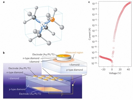
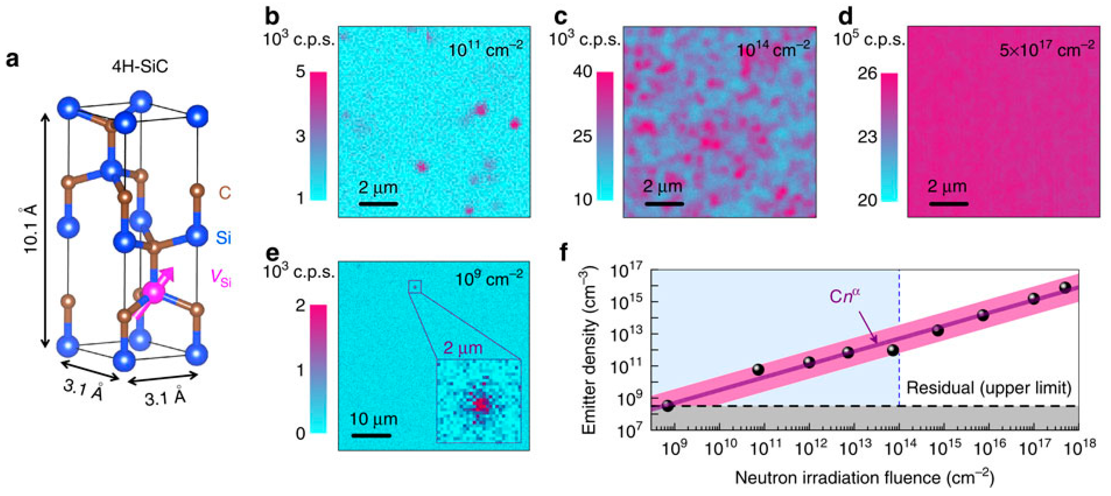
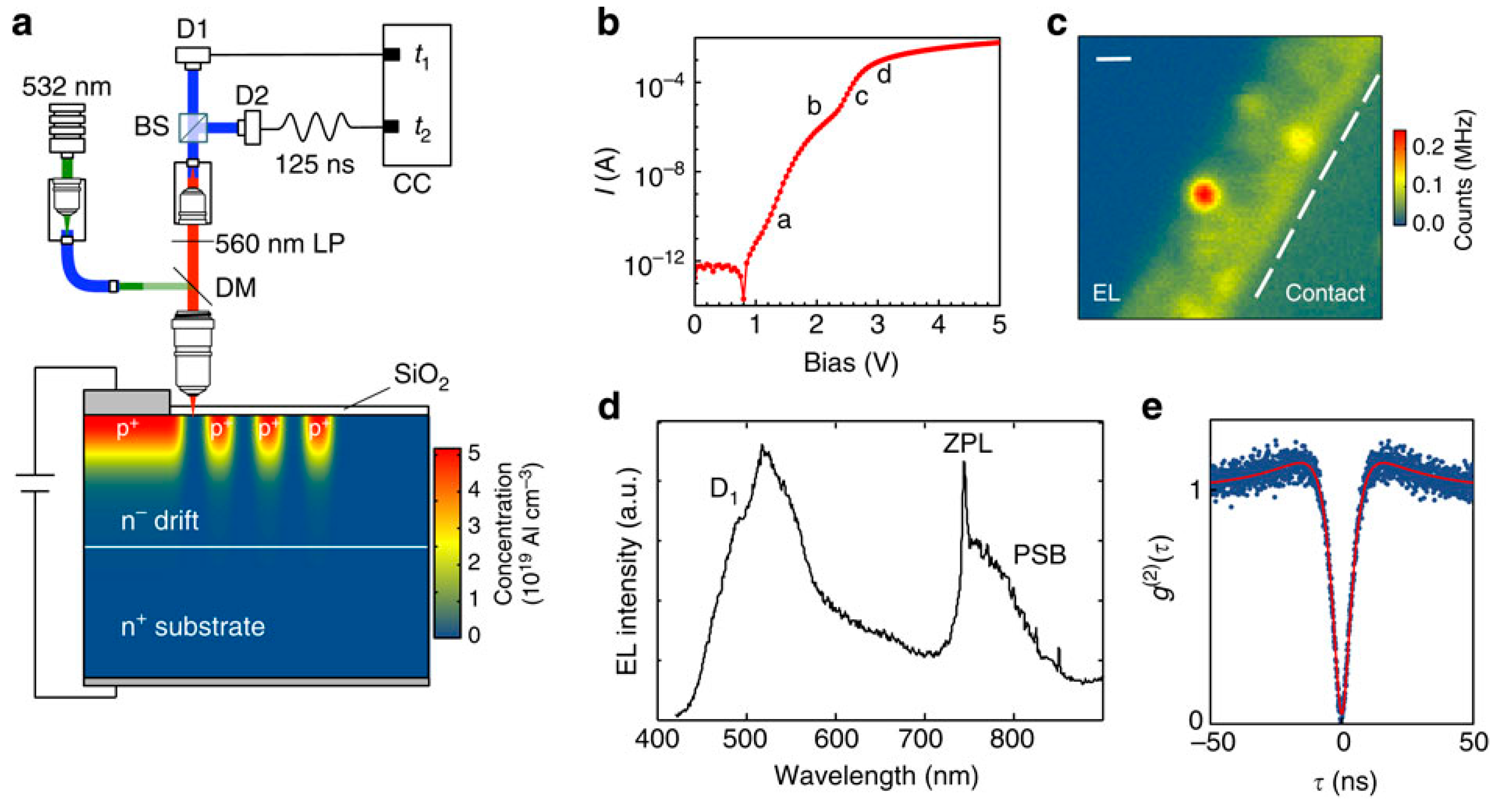
2. SiC Based Single Photon Sources

In principle, SiC as material for color centers starts with a disadvantage because of its indirect bandgap, which makes non-radiative recombination via sub-gap states more efficient than the radiative one. However, due to its broad bandgap of up to 3.3 eV in 4H polytype, SiC possesses many defects or color centers that can be exploited as isolated systems for quantum light generation [11].
Recently, bright room temperature single photon emission has been identified in bulk 4H-SiC and 3C-SiC nanoparticles [2]. This single photon emission was produced by the radiative recombination of the positively charged state of the carbon anti site vacancy pairs CSiVC. The neutral defect has been shown to possess a high spin ground state in 4H-SiC, indicating the possibility for the coherent manipulation of the electron spin as a solid state quantum bit by optical excitation of this defect at telecom wavelengths [12]. Such effects are not limited to the three most common SiC polytypes, as recent research revealed uniaxially oriented silicon vacancy-related centers with S = 3/2 in a rhombic 15R-SiC crystalline matrix, that exhibit unique features such as optical spin alignment up to temperatures around 250 °C [13].
6H-SiC single p-n junction LEDs have been proven to be functional for an ensemble of deep level defects within the material bandgap, the silicon vacancy, and a common highly thermally stable color center in all SiC poly types, the D1 center, attributed to a SiCCsi antisite [14]. Other paramagnetic defects responsible for emission at longer wavelengths have also been identified. These advances make the material attractive for electrically driven devices providing room temperature quantum light sources [11]. Such paramagnetic defects in 4H- and 6H-SiC were recently demonstrated to be strongly coupled to 29Si nuclear spins. With a 99% ± 1% degree of nuclear polarization at room temperature and an effective nuclear temperature of 5 μK, they have applications in SiC-based quantum memories [15]. Moreover, optical and microwave techniques similar to those used with diamond nitrogen-vacancy qubits, have been used to study the spin-1 ground state of the neutral carbon-silicon divacancy in 4H-SiC, which could be optically controlled at 20 to 300 K temperature, and also optically active defect spin states near telecommunication wavelengths, which, combined with industrial-scale crystal growth and advanced microfabrication techniques, and spin coherence properties comparable to the nitrogen-vacancy center can be used in a variety of photonic and quantum information applications [16].
In order to build effective quantum memory systems, one way is to achieve all-optical control of spin ensembles, and transfer the quantum states between spins and photons via coherent population trapping. Such direct all-optical addressing through magneto-spectroscopy has been recently reported in basal plane-oriented divacancy spins in 4H-SiC, in which the spin triplet structure of ground and excited states have been used to tune the transition dipole moments between spin levels, showing coherent population trapping along particular crystal axes [17].
SiC bulk material also shows promising results for room temperature electrical quantum sources in the visible and possibly in the infrared [18], although low temperatures of around 40 K may be necessary. Coherent control at room temperature of a single defect spin from single silicon vacancies in SiC has finally been demonstrated by characterizing photoluminescence and optical spin polarization [19]. Bulk SiC is also attractive for bio-applications as an in vivo luminescent marker, and for sensing magnetic field and temperature. To this end, recently, SiC nanocrystals were fabricated with sizes between 600 nm and 60 nm, and neutron irradiation was used to create silicon vacancies that showed near infrared photoluminescence and detectable room-temperature spin resonances [20].
The latest observations [21] of single defect systems with electrically controlled quantum functionalities further strengthen the position of SiC as the candidate for the preferred quantum material. Reference [21] demonstrates the fabrication of bright room temperature single photon emitting diodes having fully polarized output, superior photon statistics, and stability in continuous and pulsed modes, all at room temperature. Figure 2 presents a scheme of the confocal setup used to characterize the single-photon emitters of Reference [21]. The figure also presents the current vs. voltage properties of the diode, the electroluminescence (EL) map of the edge region of a device, the room temperature EL spectrum and the background corrected anti-bunching traces with g(2)(τ = 0) < 0.1. The image is reprinted by permission from Reference [21], copyright 2015, Macmillan Publishers Ltd.: Nature Communications.
The practicality of the single photon emission is enhanced by the electrical rather than the optical pumping. The high active n-type concentration is created by ion implantation. In Reference [21], the single photon emitters in the visible spectral range are integrated into 4H-SiC and 6H-SiC p+n and n+p junction diodes. These single photon emitting diodes are fabricated by applying well developed CMOS (Complementary Metal Oxide Semiconductor) compatible processes including photolithography, ion implantation and annealing. The quantum nature of the single defect is proven by the photon anti-bunching measurements. The emitters are shown to have high emission rates, be fully polarized and operate with high stability at room temperature.
Reference [22] shows the opportunity to create silicon vacancies in a nuclear reactor while controlling their density within an accuracy down to a single vacancy level. The isolated silicon vacancy from this latter demonstration of manufacturability is then used as a near-infrared photostable single-photon emitter with the vacancy spins being manipulated by using optically detected magnetic resonance (ODMR) methods.
Figure 3 is the generation of silicon vacancy VSi defects in ultrapure 4H-SiC samples by neutron irradiation from Reference [22]. The image is reprinted by permission from Reference [22], copyright 2015, Macmillan Publishers Ltd.: Nature Communications. The control of spin center density in ultrapure SiC is obtained by neutron irradiation over eight orders of magnitude, from below 109 to above 1016 cm−3. A fully photostable, room-temperature, near infrared single photon emitter is isolated for a low irradiation dose with no bleaching after 1014 excitation cycles. The work demonstrates the possibility of on demand engineering optically active spins in technologically friendly, biocompatible materials.
VSi defects in 4H-SiC have also recently been characterized by room-temperature ODMR to find a strong magnetic field dependence of the spin echo properties, useful in magnetometry applications. The spin echo decay time was up to 80 μs at 68 mT, with a strong field-dependent spin echo modulation attributed to the interaction with nuclear spins [23]. It was also recently observed that 4H- and 6H-SiC crystals can contain separately addressable spin-3/2 centers which are not affected by nonaxial strain fluctuations. For some of them, the axial crystal field was almost independent from temperature, which is useful for vector magnetometry. For others, the zero-field splitting showed a very high room-temperature thermal shift of 1.1 MHz/K, making them attractive for thermometry applications [24].
Other than with magnetic fields, the defect spin can also be coherently driven with alternating electric fields, permitting spatially confined spin control and the imaging of electric fields at GHz frequencies. Electrically-driven ODMR (EODMR) offers the possibility to control the electron spins in a dense array in a scalable way [25].

3. Conclusions

The achievements in References [21,22] demonstrate that SiC is the perfect material for integration between active single defects of quantum systems and existing device technologies operating at room temperature.
By integrating electron spin-states and single photons in monolithic and nanostructured SiC devices, novel imaging and sensing modalities that combine several quantum degrees of freedom, namely optical, spin and mechanical, may therefore be developed to enhance the sensitivity of conventional devices from the classical domain to the quantum domain.
As the SiC devices benefit from an unprecedented sensitivity due to the integration, control and coupling of inherent single spin and single optical quantum modes with electrical and mechanical modalities intrinsic of the device, it is now a certainty that SiC is gaining momentum for atomic-scale spintronics and quantum technologies.

Acknowledgments

This research did not receive any specific grant from funding agencies in the public, commercial, or not-for-profit sectors.

Author Contributions

Both authors equally contributed to the reported research and writing of the paper. Both authors have read and approved the final manuscript.

Conflicts of Interest

The author declares no conflict of interest.

References

  1. Castelletto, S.; Johnson, B.C.; Boretti, A. Quantum effects in silicon carbide hold promise for novel integrated devices and sensors. Adv. Opt. Mater. 2013, 1, 609–625. [Google Scholar] [CrossRef]
  2. Castelletto, S.; Johnson, B.C.; Ivády, V.; Stavrias, N.; Umeda, T.; Gali, A.; Ohshima, T. A silicon carbide room-temperature single-photon source. Nat. Mater. 2014, 13, 151–156. [Google Scholar] [CrossRef] [PubMed]
  3. Petta, J.R.; Johnson, A.C.; Taylor, J.M.; Laird, E.A.; Yacoby, A.; Lukin, M.D.; Marcus, C.M.; Hanson, M.P.; Gossard, A.C. Coherent manipulation of coupled electron spins in semiconductor quantum dots. Science 2005, 309, 2180–2184. [Google Scholar] [CrossRef] [PubMed]
  4. Hofheinz, M.; Wang, H.; Ansmann, M.; Bialczak, R.C.; Lucero, E.; Neeley, M.; O’Connell, A.D.; Sank, D.; Wenner, J.; Martinis, J.M.; et al. Synthesizing arbitrary quantum states in a superconducting resonator. Nature 2009, 459, 546–549. [Google Scholar] [CrossRef] [PubMed]
  5. Pla, J.J.; Tan, K.Y.; Dehollain, J.P.; Lim, W.H.; Morton, J.J.L.; Jamieson, D.N.; Dzurak, A.S.; Morello, A. A single-atom electron spin qubit in silicon. Nature 2012, 489, 541–545. [Google Scholar] [CrossRef] [PubMed]
  6. Bounouar, S.; Elouneg-Jamroz, M.; den Hertog, M.; Morchutt, C.; Bellet-Amalric, E.; André, R.; Bougerol, C.; Genuist, Y.; Poizat, J.-P.; Tatarenko, S.; et al. Ultrafast room temperature single-photon source from nanowire-quantum dots. Nano Lett. 2012, 12, 2977–2981. [Google Scholar] [CrossRef] [PubMed]
  7. Holmes, M.J.; Choi, K.; Kako, S.; Arita, M.; Arakawa, Y. Room-temperature triggered single photon emission from a III-nitride site-controlled nanowire quantum dot. Nano Lett. 2014, 14, 982–986. [Google Scholar] [CrossRef] [PubMed]
  8. Yuan, Z.; Kardynal, B.E.; Stevenson, R.M.; Shields, A.J.; Lobo, C.J.; Cooper, K.; Beattie, N.S.; Ritchie, D.A.; Pepper, M. Electrically driven single-photon source. Science 2002, 295, 102–105. [Google Scholar] [CrossRef] [PubMed]
  9. Mizuochi, N.; Kato, H.; Takeuchi, D.; Ogura, M.; Okushi, H.; Nothaft, M.; Neumann, P.; Gali, A.; Jelezko, F.; Wrachtrup, J.; et al. Electrically driven single-photon source at room temperature in diamond. Nat. Photon. 2012, 6, 299–303. [Google Scholar] [CrossRef]
  10. Castelletto, S.; Rosa, L.; Johnson, B.C. Silicon carbide for novel quantum technology devices. In Advanced Silicon Carbide Devices and Processing; Saddow, S., La Via, F., Eds.; InTech: Rijeka, Croatia, 2015. [Google Scholar]
  11. Boretti, A.; Rosa, L.; Mackie, A.; Castelletto, S. Electrically driven quantum light sources. Adv. Opt. Mater. 2015, 3, 1012–1033. [Google Scholar] [CrossRef]
  12. Szász, K.; Ivády, V.; Abrikosov, I.A.; Janzén, E.; Bockstedte, M.; Gali, A. Spin and photophysics of carbon-antisite vacancy defect in 4H silicon carbide: A potential quantum bit. Phys. Rev. B 2015, 91, 121201. [Google Scholar] [CrossRef]
  13. Soltamov, V.A.; Yavkin, B.V.; Tolmachev, D.O.; Babunts, R.A.; Badalyan, A.G.; Davydov, V.Y.; Mokhov, E.N.; Proskuryakov, I.I.; Orlinskii, S.B.; Baranov, P.G. Optically addressable silicon vacancy-related spin centers in rhombic silicon carbide with high breakdown characteristics and endor evidence of their structure. Phys. Rev. Lett. 2015, 115, 247602. [Google Scholar] [CrossRef] [PubMed]
  14. Fuchs, F.; Soltamov, V.A.; Väth, S.; Baranov, P.G.; Mokhov, E.N.; Astakhov, G.V.; Dyakonov, V. Silicon carbide light-emitting diode as a prospective room temperature source for single photons. Sci. Rep. 2013, 3, 1637. [Google Scholar] [CrossRef] [PubMed]
  15. Falk, A.L.; Klimov, P.V.; Ivády, V.; Szász, K.; Christle, D.J.; Koehl, W.; Gali, A.; Awschalom, D.D. Optical polarization of nuclear spins in silicon carbide. Phys. Rev. Lett. 2015, 114, 247603. [Google Scholar] [CrossRef] [PubMed]
  16. Koehl, W.F.; Buckley, B.B.; Heremans, F.J.; Calusine, G.; Awschalom, D.D. Room temperature coherent control of defect spin qubits in silicon carbide. Nature 2011, 479, 84–87. [Google Scholar] [CrossRef] [PubMed]
  17. Zwier, O.V.; O’Shea, D.; Onur, A.R.; van der Wal, C.H. All-optical coherent population trapping with defect spin ensembles in silicon carbide. Sci. Rep. 2015, 5, 10931. [Google Scholar] [CrossRef] [PubMed]
  18. Christle, D.J.; Falk, A.L.; Andrich, P.; Klimov, P.V.; Hassan, J.U.; Son, N.T.; Janzén, E.; Ohshima, T.; Awschalom, D.D. Isolated electron spins in silicon carbide with millisecond coherence times. Nat. Mater. 2015, 14, 160–163. [Google Scholar] [CrossRef] [PubMed]
  19. Widmann, M.; Lee, S.-Y.; Rendler, T.; Son, N.T.; Fedder, H.; Paik, S.; Yang, L.-P.; Zhao, N.; Yang, S.; Booker, I.; et al. Coherent control of single spins in silicon carbide at room temperature. Nat. Mater. 2015, 14, 164–168. [Google Scholar] [CrossRef] [PubMed]
  20. Muzha, A.; Fuchs, F.; Tarakina, N.V.; Simin, D.; Trupke, M.; Soltamov, V.A.; Mokhov, E.N.; Baranov, P.G.; Dyakonov, V.; Krueger, A.; et al. Room-temperature near-infrared silicon carbide nanocrystalline emitters based on optically aligned spin defects. Appl. Phys. Lett. 2014, 105, 243112. [Google Scholar] [CrossRef]
  21. Lohrmann, A.; Iwamoto, N.; Bodrog, Z.; Castelletto, S.; Ohshima, T.; Karle, T.J.; Gali, A.; Prawer, S.; McCallum, J.C.; Johnson, B.C. Single-photon emitting diode in silicon carbide. Nat. Commun. 2015, 6, 7783. [Google Scholar] [CrossRef] [PubMed]
  22. Fuchs, F.; Stender, B.; Trupke, M.; Simin, D.; Pflaum, J.; Dyakonov, V.; Astakhov, G.V. Engineering near-infrared single-photon emitters with optically active spins in ultrapure silicon carbide. Nat. Commun. 2015, 6, 7578. [Google Scholar] [CrossRef] [PubMed]
  23. Carter, S.G.; Soykal, Ö.O.; Dev, P.; Economou, S.E.; Glaser, E.R. Spin coherence and echo modulation of the silicon vacancy in 4H-SiC at room temperature. Phys. Rev. B 2015, 92, 161202. [Google Scholar] [CrossRef]
  24. Astakhov, G.V.; Kraus, H.; Soltamov, V.A.; Fuchs, F.; Simin, D.; Sperlich, A.; Baranov, P.G.; Dyakonov, V. Magnetic field and temperature sensing with atomic-scale spin defects in silicon carbide. Sci. Rep. 2014, 4, 5303. [Google Scholar] [CrossRef]
  25. Klimov, P.V.; Falk, A.L.; Buckley, B.B.; Awschalom, D.D. Electrically driven spin resonance in silicon carbide color centers. Phys. Rev. Lett. 2014, 112, 087601. [Google Scholar] [CrossRef]
Figure 1. (a) Atomic structure of an NV center in diamond; (b) Schematic of the single photon emitting diode; (c) Current vs. voltage properties of the p–i–n junction in a log plot. Reprinted by permission from Reference [9], copyright 2012, Macmillan Publishers Ltd.: Nature Photonics.
Technologies 04 00016 g001
Figure 2. (a) Schematic of the confocal setup used to characterize the single-photon emitters; (b) Current-Voltage curve of the diode; (c) electroluminescence (EL) map of the edge region of a device; (d) room temperature EL spectrum; (e) background corrected anti-bunching traces with g(2)(τ = 0) < 0.1. Reprinted by permission from Reference [21], copyright 2015, Macmillan Publishers Ltd.: Nature Communications.
Technologies 04 00016 g002
Figure 3. (a) scheme of the 4H-SiC with the single VSi defect; (bd) confocal microscopy scans 10 × 10 μm2 for different neutron irradiation doses respectively n = 1 × 1011 cm−2, n = 1 × 1014 cm−2 and n = 5 × 1017 cm−2; (e) confocal microscopy scan 50 × 50 μm2 for n = 1 × 109 cm−2; (f) concentration of single photon emitters vs. the irradiation dose. Reprinted by permission from Reference [22], copyright 2015, Macmillan Publishers Ltd.: Nature Communications.
Technologies 04 00016 g003

