
Electrically Injected Twin Photon Emitting Lasers at Room Temperature

Abstract
:
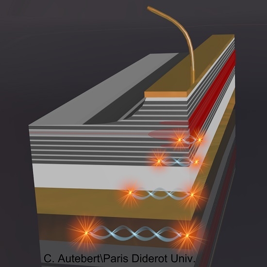
1. Introduction
2. Results
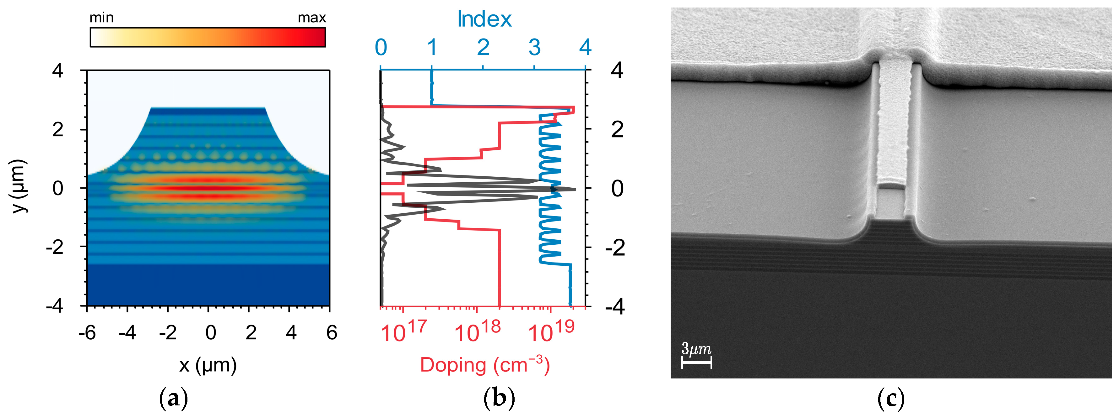
2.1. Design and Fabrication
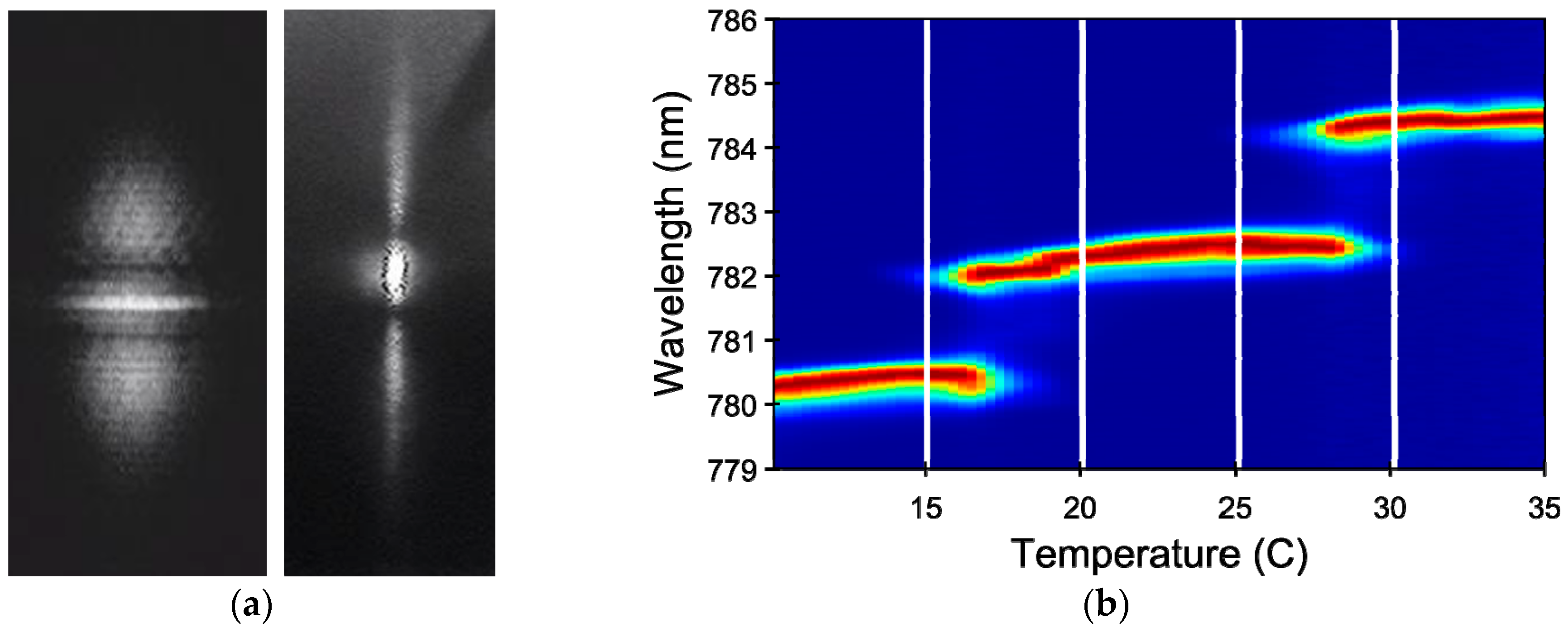
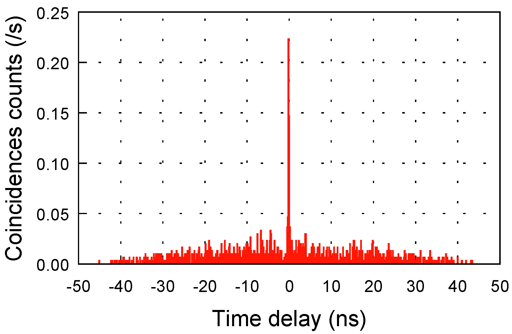
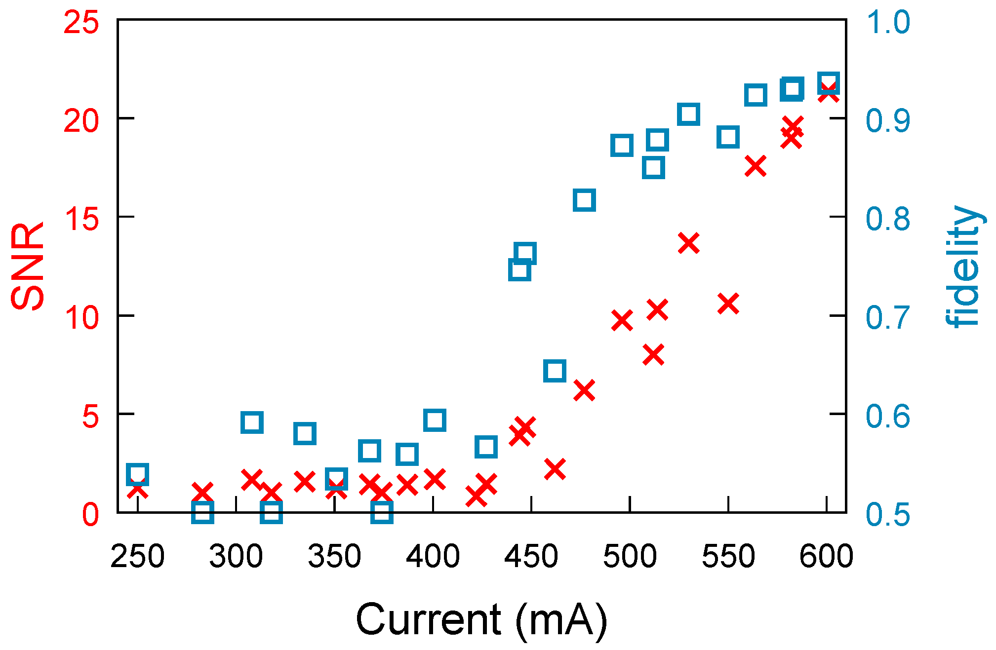
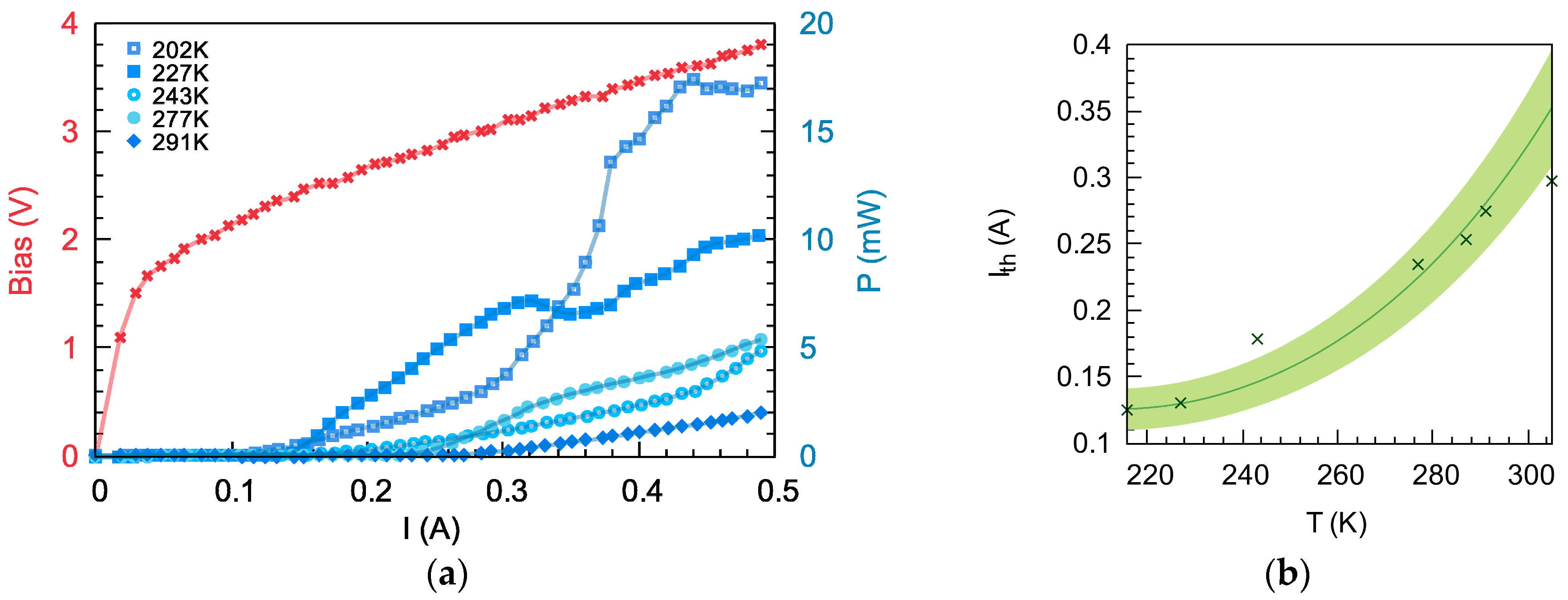
2.2. Optoelectronic Characterization
3. Discussion and Conclusions
Acknowledgments
Author Contributions
Conflicts of Interest
References
- Grassani, D.; Azzini, S.; Liscidini, M.; Galli, M.; Strain, M.J.; Sorel, M.; Sipe, J.E.; Bajoni, D. MicRometer-scale integrated silicon source of time-energy entangled photons. Optica 2015, 2, 88–94. [Google Scholar] [CrossRef]
- Matthews, J.C.F.; Politi, A.; Stefanov, A.; O’Brien, J.L. Manipulation of multiphoton entanglement in waveguide quantum circuits. Nat. Photonics 2009, 3, 346–350. [Google Scholar] [CrossRef]
- Spagnolo, N.; Vitelli, C.; Bentivegna, M.; Brod, D.J.; Crespi, A.; Flamini, F.; Giacomini, S.; Milani, G.; Ramponi, R.; Mataloni, P.; et al. Experimental validation of photonic boson sampling. Nat. Photonics 2014, 8, 615–620. [Google Scholar] [CrossRef]
- Spring, J.B.; Metcalf, B.J.; Humphreys, P.C.; Kolthammer, W.S.; Jin, X.M.; Barbieri, M.; Datta, A.; Thomas-Peter, N.; Langford, N.K.; Kundys, D.; et al. Boson sampling on a photonic chip. Science 2013, 339, 798–799. [Google Scholar] [CrossRef] [PubMed]
- Sprengers, J.P.; Gaggero, A.; Sahin, D.; Jahanmirinejad, S.; Frucci, G.; Mattioli, F.; Leoni, R.; Beetz, J.; Lermer, M.; Kamp, M.; et al. Waveguide superconducting single-photon detectors for integrated quantum photonic circuits. Appl. Phys. Lett. 2011, 99, 181110. [Google Scholar] [CrossRef]
- Somaschi, N.; Giesz, V.; de Santis, L.; Loredo, J.C.; Almeida, M.P.; Hornecker, G.; Portalupi, S.L.; Grange, T.; Antón, C.; Demory, J.; et al. Near-optimal single-photon sources in the solid state. Nat. Photonics 2016, 10, 340–345. [Google Scholar] [CrossRef]
- Boitier, F.; Orieux, A.; Autebert, C.; Lemaitre, A.; Galopin, E.; Manquest, C.; Sirtori, C.; Favero, I.; Leo, G.; Ducci, S. Electrically injected photon-pair source at room temperature. Phys. Rev. Lett. 2014, 112, 183901. [Google Scholar] [CrossRef] [PubMed]
- Shoji, I.; Kondo, T.; Ito, R. Second-order nonlinear susceptibilities of various dielectric and semiconductor materials. Opt. Quantum Electron. 2002, 34, 797–833. [Google Scholar] [CrossRef]
- Yeh, P.; Yariv, A. Bragg reflection waveguides. Opt. Commun. 1976, 19, 427–430. [Google Scholar] [CrossRef]
- Helmy, A.; Bijlani, B.; Abolghasem, P. Phase matching in monolithic Bragg reflection waveguides. Opt. Lett. 2007, 32, 2399–2401. [Google Scholar] [CrossRef] [PubMed]
- Rossi, A.D.; Ortiz, V.; Calligaro, M.; Vinter, B.; Nagle, J.; Ducci, S.; Berger, V. A third-order-mode laser diode for quantum communication. Semicond. Sci. Technol. 2004, 19, L99–L102. [Google Scholar] [CrossRef]
- Autebert, C.; Boucher, G.; Boitier, F.; Eckstein, A.; Favero, I.; Leo, G.; Ducci, S. Photon pair sources in algaas: From electrical injection to quantum state engineering. J. Mod. Opt. 2015, 62, 1739–1745. [Google Scholar] [CrossRef]
- Svelto, O.; Hanna, D.C. Principles of Lasers, 5th ed.; Springer: Berlin, Gemany, 2012. [Google Scholar]
- Ravaro, M.; Guillotel, E.; Le Dû, M.; Manquest, C.; Marcadet, X.; Ducci, S.; Berger, V.; Leo, G. Nonlinear measurement of mid-infrared absorption in AlOx waveguides. Appl. Phy. Lett. 2008, 92, 151111. [Google Scholar] [CrossRef]
- Lumerical Solutions, I. Available online: http://www.lumerical.com/tcad-products/fdtd (accessed on 25 June 2016).
- Marvin, D.C.; Moss, S.C.; Halle, L.F. Analysis of transient photoluminescence measurements on GaAs and AlGaAs double heterostructures. J. Appl. Phys. 1992, 72, 1970–1984. [Google Scholar] [CrossRef]
- Lanco, L. Sources Semiconductrices de Photons Jumeaux. Ph.D. Thesis, Université Paris Diderot, Paris, France, 2006. [Google Scholar]
- Chinone, N.; Kuroda, T.; Ohtoshi, T.; Takahashi, T.; Kajimura, T. Mode-hopping noise in index-guided semiconductor lasers and its reduction by saturable absorbers. IEEE J. Quantum Electron. 1985, 21, 1264–1270. [Google Scholar] [CrossRef]
- Copeland, J. Single-mode stabilization by traps in semiconductor lasers. IEEE J. Quantum Electron. 1980, 16, 721–727. [Google Scholar] [CrossRef]
- Autebert, C.; Lemaître, A.; Ducci, S. Highly efficient parametric down conversion in a monolithic AlGaAs waveguide. 2016; in preparation. [Google Scholar]
- Günthner, T.; Pressl, B.; Laiho, K.; Geßler, J.; Höfling, S.; Kamp, M.; Schneider, C.; Weihs, G. Broadband indistinguishability from bright parametric downconversion in a semiconductor waveguide. J. Opt. 2015, 17, 125201. [Google Scholar] [CrossRef]
- Autebert, C.; Bruno, N.; Martin, A.; Lemaitre, A.; Carbonell, C.G.; Favero, I.; Leo, G.; Zbinden, H.; Ducci, S. Integrated algaas source of highly indistinguishable and energy-time entangled photons. Optica 2016, 3, 143–146. [Google Scholar] [CrossRef]
- Horn, R.T.; Kolenderski, P.; Kang, D.; Abolghasem, P.; Scarcella, C.; Della Frera, A.; Tosi, A.; Helt, L.G.; Zhukovsky, S.V.; Sipe, J.E.; et al. Inherent polarization entanglement generated from a monolithic semiconductor chip. Sci. Rep. 2013, 3, 2314. [Google Scholar] [CrossRef] [PubMed] [Green Version]
- Autebert, C.; Trapateau, J.; Orieux, A.; Lemaitre, A.; Carbonell, C.G.; Diamanti, E.; Zaquine, I.; Ducci, S. Multi-User Quantum Key Distribution with Entangled Photons from an AlGaAs Chip. 2016. Available online: http://arxiv.org/abs/1607.01693 (accessed on 6 July 2016).
- Svozilyk, J.; Hendrych, M.; Helmy, A.S.; Torres, J.P. Generation of paired photons in a quantum separable state in Bragg reflection waveguides. Opt. Express 2011, 19, 3115–3123. [Google Scholar] [CrossRef] [PubMed]


© 2016 by the authors; licensee MDPI, Basel, Switzerland. This article is an open access article distributed under the terms and conditions of the Creative Commons Attribution (CC-BY) license (http://creativecommons.org/licenses/by/4.0/).
Share and Cite
Autebert, C.; Maltese, G.; Halioua, Y.; Boitier, F.; Lemaître, A.; Amanti, M.; Sirtori, C.; Ducci, S. Electrically Injected Twin Photon Emitting Lasers at Room Temperature. Technologies 2016, 4, 24. https://doi.org/10.3390/technologies4030024
Autebert C, Maltese G, Halioua Y, Boitier F, Lemaître A, Amanti M, Sirtori C, Ducci S. Electrically Injected Twin Photon Emitting Lasers at Room Temperature. Technologies. 2016; 4(3):24. https://doi.org/10.3390/technologies4030024
Chicago/Turabian StyleAutebert, Claire, Giorgio Maltese, Yacine Halioua, Fabien Boitier, Aristide Lemaître, Maria Amanti, Carlo Sirtori, and Sara Ducci. 2016. "Electrically Injected Twin Photon Emitting Lasers at Room Temperature" Technologies 4, no. 3: 24. https://doi.org/10.3390/technologies4030024