Article

Marmote SDR: Experimental Platform for Low-Power Wireless Protocol Stack Research

Institute for Software Integrated Systems, Vanderbilt University, 1025 16th Ave S, Nashville, TN 37212, USA
*
Authors to whom correspondence should be addressed.
J. Sens. Actuator Netw. 2013, 2(3), 631-652; https://doi.org/10.3390/jsan2030631
Submission received: 10 July 2013 / Revised: 20 August 2013 / Accepted: 27 August 2013 / Published: 9 September 2013
(This article belongs to the Special Issue Feature Papers)

Abstract

:
Over the past decade, wireless sensor network research primarily relied on highly-integrated commercial off-the-shelf radio chips. The rigid silicon implementation of the radio stack restricted access to the lower layers; thus, research focused mainly on the medium access control (MAC) layer and above. SRAM field-programmable gate array (FPGA)-based software-defined radios (SDR), on the other hand, provide a flexible architecture to experiment with any and all layers of the radio stack, but usually require desktop computers and draw high currents that prohibit mobile or longer-term outdoor deployments. To address these issues, we have developed a modular flash FPGA-based wireless research platform, called Marmote SDR, that has computational resources comparable to those of SRAM FPGA-based radio platforms, but at a reduced power consumption, with duty cycling support. We discuss the design decisions underlying Marmote SDR and evaluate its power consumption. Furthermore, we present and evaluate an asynchronous and multiple access communication protocol specifically designed for data-gathering wireless sensor networks.

Graphical Abstract

1. Introduction

Wireless sensor network (WSN) nodes of the past decade have traditionally been designed with a simple system concept in mind: application-specific sensors attached to a general platform that provides computational resources and wireless connectivity. Successful platforms, such as the MICAz [1] and TelosB [2] motes, are representative examples of this architecture, as both employ simple microcontrollers and integrated short-range radio frequency (RF) transceiver chips.
The ultra-low-power requirement of these WSN nodes is usually addressed by optimizing the consumption of the microcontroller and the RF chip. The 30–60 mW order power demand of wireless communication, however, gradually overwhelms that of the microprocessor performing the sensor level digital signal processing, which is typically below 10 mW [3,4,5]. RF-related energy saving in multi-hop networks is almost exclusively achieved in the medium access control (MAC) layer by efficient scheduling of single-hop packet transmission and reception, e.g., via duty cycling. One major reason for this is that commonly used RF chips come as application-specific integrated circuits (ASIC). They primarily provide a packet level interface and prescribe a carrier sense multiple access (CSMA) or time division multiple access (TDMA)-based scheme, restricting access to the lower layers, hence, imposing inflexibility.
Software-defined radio (SDR), on the other hand, is a well developed technology that emphasizes the design flexibility of communication protocols. Commercially available SDR platforms connected to desktop computers enable the development of complex and full vertical radio communication stacks with acceptable engineering effort. However, the design flexibility of such SDR platforms comes at a price in the power consumption budget (typically over 10 W) and in physical dimensions, which generally prohibits experimentation in deployed or mobile scenarios with no wall power for any reasonable length of time.
We argue that communication-related power saving in WSNs can go beyond designing scheduling schemes defined over packet transmissions; energy consumption may be reduced significantly by tailoring the MAC and physical (PHY) layers of the communication protocol stack to a specific WSN application. Ideas can be borrowed from other fields, such as cellular telephony or satellite communication, and design flexibility can be increased by following the approach of field-programmable gate array (FPGA)-based software-defined radios. We also suggest that WSN communication-related research should not be restricted to computer simulations, often posing oversimplifying assumptions. Rather, real-world experiments should be encouraged to provide the proof of a given concept. Hence, we present a WSN research platform that provides access to the lower layers of the communication protocol stack with the design speed and flexibility of FPGA-based SDRs and, at the same time, allows for deployed battery-based operation spanning multiple days.
Leveraging the flexibility of this platform, we implemented a simple frequency shift keying (FSK) PHY layer design to provide a power consumption comparison with existing commercial integrated RF chips and SDRs in typical WSN operating modes. We present the design and experimental evaluation of the PHY layer of a more sophisticated spread-spectrum WSN communication protocol. In particular, we propose the use of a direct-sequence spread spectrum (DSSS)-based code division multiple access (DS-CDMA) scheme to provide asynchronous, collision-free medium access for the sensor nodes in the base station vicinity, as the experimental evaluation of such schemes has been largely unaddressed in the WSN literature.
In the remainder of the paper, we first discuss the background and related work. In Section 3, we present the hardware design of the Marmote SDR platform. We present a preliminary evaluation of the platform’s power consumption in Section 4. Then, we discuss the DSSS communication protocol in Section 5 and conclude in Section 6.

2. Background and Related Work
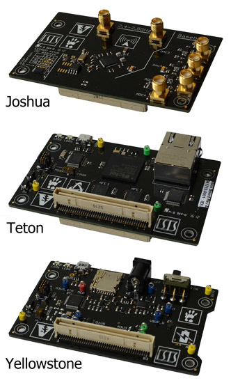
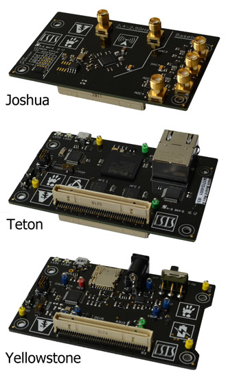
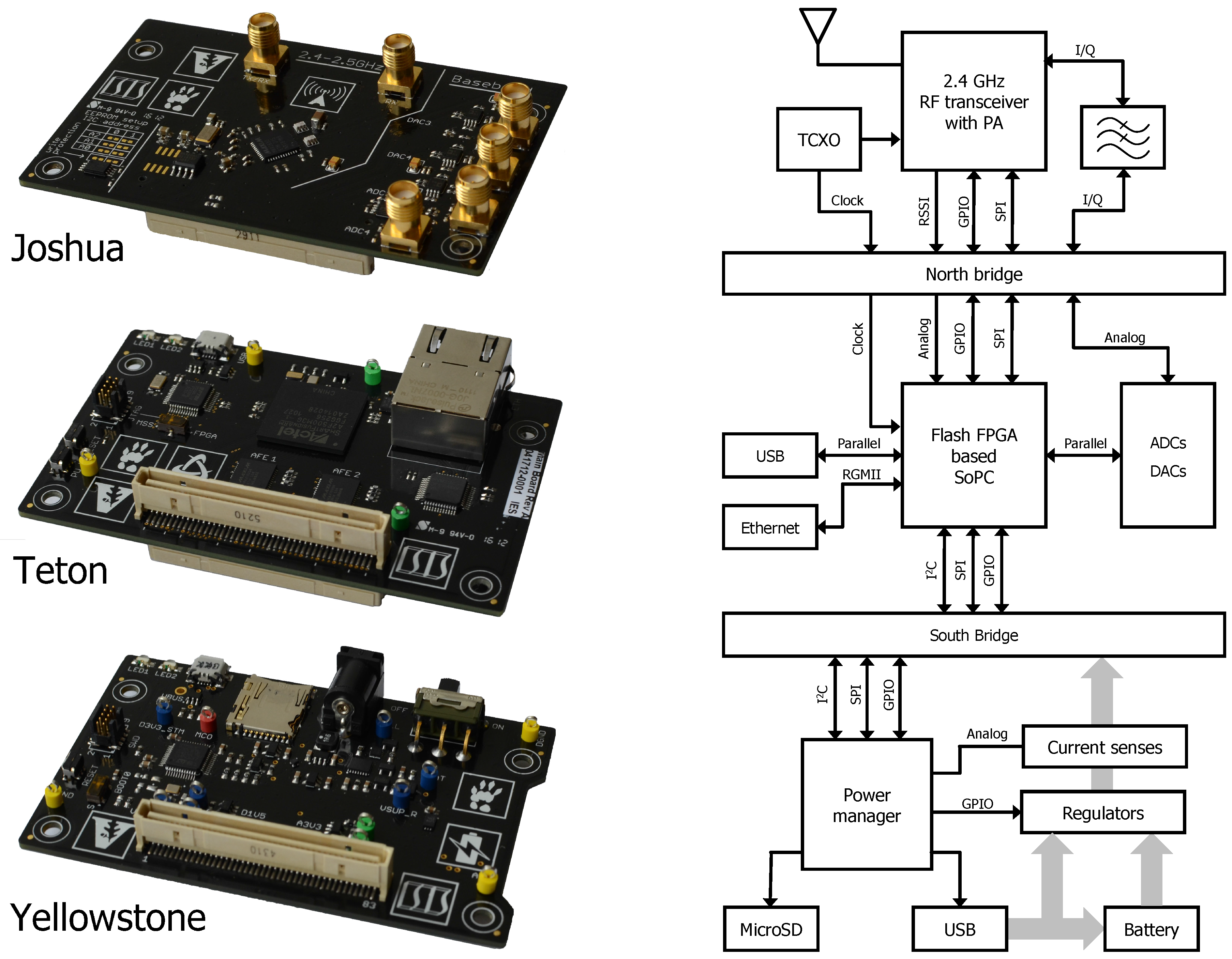
The WSN communication protocol stack has been extensively investigated in the past decade, with a special focus on the MAC layer. Muneeb Ali et al. summarize former research efforts and optimization criteria in [6] and give suggestions on future directions. They argue that as energy consumption of computing chips falls more sharply than that of the radio front-ends, the wireless interface becomes the primary consumer of energy in WSN nodes. Therefore, designing the wireless protocol stack for energy efficiency should be treated with the utmost importance in WSNs among other traditional goals, such as fairness, delay or bandwidth utilization. They also point out that research tools should be carefully chosen and real-world experiments should be preferred over ns-2 and OMNeT++ simulations that often make unreasonably simplified assumptions. For the former, Muneeb Ali et al. advocates the use of SDRs, which would give access to the stack layers below the MAC.
One significant step towards SDR-based experimentation was the SoftMAC [7] software architecture developed by Neufeld et al. on top of an IEEE 802.11 compliant Atheros network card. They reverse-engineered portions of the Atheros AR5212 chip interface and wrote a software driver that gives extensive access to the MAC layer and partial control over the PHY layer. The greatest benefit of this approach is the reduced SDR hardware cost, due to the use of commodity chips. However, the flexibility of SoftMAC is limited compared to a full-stack SDR, as the former has control over only a small part of the PHY layer.
Full-stack SDRs saw a constant rise in popularity during the past decade. Complete software tool suites, such as Matlab and Simulink or the open-source GNU Radio [8], are available for researchers to develop complete vertical protocol stacks with reasonable development effort and design cycle. These software tools can seamlessly connect to mid-priced SDR hardware, such as the USRP [9] SDRs from Ettus Research. The USRP N210 hardware contains an SRAM FPGA responsible for a fixed set of low-level baseband signal processing tasks, while the rest of the wireless stack is processed on an Ethernet or USB connected desktop PC. Simulink also allows one to target high-end general FPGA development platforms from Xilinx and Altera connected to an FPGA mezzanine card radio front-end and a PC, to generate prototype FPGA configuration from model blocks in an automated fashion [10]. The clear advantage of such desktop SDRs is that they allow full control of the entire network stack, including the complete baseband processing, at the cost of an affordable development time. The cost and power consumption of such platforms and the need for a PC connection, however, severely limits their use in deployed WSN scenarios.
The flexibility and the ASIC-class parallel processing capability made SRAM FPGAs attractive for WSNs, as well. Several WSN nodes utilizing SRAM FPGAs have been developed and extensively used in various applications, such as human body movement tracking [11], safety-related systems [12] and shooter localization [13]. Valverde et al. recently investigated the performance and energy consumption of a mid-size SRAM FPGA-based WSN platform in [14]. Thus, it is clearly indicated that FPGAs are an emerging alternative to high-end microcontrollers and digital signal processors in computationally-intensive WSN applications. Furthermore, SDR hardware designs of SDR4All [15] and OsmoSDR [16] demonstrate that even relatively small-size SRAM FPGAs are capable of significant baseband signal processing. SRAM FPGAs, however, offer very limited options when it comes to low-power duty-cycle modes. Transitioning from sleep to active mode is delayed and energy demanding, because the volatile SRAM configuration cells need to be reconfigured on every wake-up. Furthermore, their static power consumption is relatively large compared to FPGAs manufactured with flash and antifuse technologies. For comparison, the static current draw of the Xilinx Spartan-6 LX16 SRAM FPGA is 6 mA at 1.25 V, whereas that of the similar-sized Microsemi IGLOO AGL600 flash FPGA is two orders of magnitude smaller, only 30 μA at 1.2 V, based on datasheet reported values.
Flash FPGA architectures offer reasonable processing power with favorable power saving features. We have formerly developed an application-specific WSN node for structural health monitoring [17] that employed a Microsemi (formerly Actel) IGLOO flash FPGA, relying on its instant-on startup and clock scaling capabilities. A similar flash FPGA-based node architecture has recently been investigated by Nyländen et al. In [18], they compare an Altera Cyclone III SRAM FPGA and a Microsemi IGLOO flash FPGA in terms of processing performance and power consumption. They conclude, that despite the lack of hard multiplier-blocks in the flash FPGA, it still achieves reasonable energy efficiency. Philipp et al. investigated the reconfigurability of a similar, but more general, architecture in [19], also based on an IGLOO flash FPGA. Finally, Ye-Sheng Kuo et al. examined the feasibility of the 802.15.4 protocol on a flash FPGA-based architecture in [20] and found the FPGA resources sufficient, despite the lack of hardware multipliers.
In this paper, we propose a modular WSN research platform for network protocol stack development and for WSN applications that demand high-speed parallel signal processing. The Marmote SDR platform leverages our previous experiences with flash FPGAs and employs a flash FPGA-based system-on-a-programmable-chip (SoPC) backed up with high-speed, low-power analog-to-digital and digital-to-analog converters (ADCs and DACs) to interface with high-bandwidth analog signals of the analog module. While our modular approach allows for dealing with signals of various nature (e.g., acoustic), the setup presented in this paper processes baseband signals of a radio front-end, hence forming an embedded SDR. The FPGA fabric resources present in the flash FPGA-based SoPC are less abound, but still comparable to the logic in SRAM FPGAs in [15,16]. We traded this moderate performance for the advanced power saving benefits offered by the flash FPGA architecture.

3. Hardware Design

The primary driving force behind the Marmote SDR hardware design was to create a general and flexible WSN research platform that enables experimentation with various power saving techniques, such as energy harvesting, and various analog sensor and radio front-ends. Thus, the Marmote SDR platform follows a modular three-layer approach, where the radio front-end, the mixed-signal flash FPGA-based processing unit and the power supply are separated into three different modules, as shown in Figure 1. The stacked architecture makes it possible to seamlessly replace the top-layer radio front-end and the bottom-layer power supply modules, while keeping the same mixed-signal processing module intact.
Figure 1. Photo (left) and block diagram (right) of the three-layer Marmote SDR platform comprising a Joshua 2.4 GHz radio front-end (top), a Teton mixed-signal processing (middle) and a Yellowstone battery-operated power management (bottom) module.
Jsan 02 00631 g001
The Marmote SDR configuration presented in this paper includes a 2.4 GHz radio front-end, a flash FPGA SoPC-based mixed-signal processing module and a rechargeable battery-based power management module. The photo and block diagram of these modules are presented in Figure 1.

3.1. 2.4 GHz Radio Front-End

The current interchangeable top-layer module, named Joshua, is an analog radio front-end designed to operate in the 2.4 to 2.5 GHz industrial, scientific and medical (ISM) frequency band and to interface with the middle-layer mixed-signal module through a pair of analog baseband in-phase and quadrature-phase (I/Q) signals, both for transmission and reception. By interfacing with the analog baseband signals, the Joshua board not only provides access to the lower PHY layers of 802.11b/g (WLAN) and 802.15.4 (e.g., ZigBee) protocols, but also allows experimentation with various types of channel access methods, such as frequency division multiple access (FDMA), TDMA and CDMA, and different modulation techniques.
The Joshua radio front-end is built primarily around the integrated Maxim MAX2830 RF transceiver, power amplifier, receive/transmit (Rx/Tx) and antenna diversity switch and, thus, supports both single and dual-antenna setups. While we looked at many alternative RF chips, we opted for the MAX2830, for it was one of the few models that makes both the Rx and Tx baseband I/Q signals accessible. The single die integration of most RF components saves board space and reduces the overall power consumption. However, these analog components are designed for higher linearity and dynamic range requirements than the commodity low-cost RF chips, and consequently, they draw significantly more current. The MAX2830 chip also incorporates a voltage controlled oscillator and a fast settling 20 Hz step adjustable RF synthesizer. While the original goal of the precise digital tuning capability is to allow use of low-cost crystals, we chose to use the integrated crystal oscillator as a buffer and to drive it by a precise 2.5 ppm, low-power temperature compensated crystal oscillator (TCXO). The stable and accurate TCXO along with the fine adjustable synthesizer are expected to give sufficiently precise control over the local oscillator frequency for applications, where formerly, we found this to be an issue [21].
The direct conversion, zero-intermediate frequency RF-to-baseband Rx, baseband-to-RF Tx paths are also part of the RF chip, along with the programmable 7.5–18 MHz low-pass baseband filters. The analog Rx and Tx baseband signals are complex I/Q pairs digitized and processed by the ADCs/DACs and the FPGA, respectively, on the middle-layer mixed-signal processing module. While the Joshua board hosts a single RF transceiver, future Marmote SDR radio front-ends may utilize a second transceiver for multiple-input and multiple-output (MIMO) and multi-band RF applications.

3.2. Mixed-Signal Processing Module

The middle-layer of the Marmote SDR platform, called Teton, is a mixed-signal processing module that is the main building block of any Marmote SDR application. In the current setup, Teton controls the top-layer radio front-end and provides computational resources for a complete vertical network stack, including PHY layer baseband signal processing.
The basis of the mixed-signal processing module is a flash FPGA-based SoPC and two external analog front-ends (AFE) that make the module capable of simultaneously processing two sets of analog baseband I/Q signal pairs. Each set of the analog baseband I/Q Rx and Tx pairs is connected to the 10-bit ADCs and DACs of a Maxim MAX19706 type low-power AFE, respectively. While interfacing with two sets of baseband signals renders the Teton board suitable for MIMO application development with an appropriate radio front-end module, the current 2.4 GHz Joshua RF module contains only a single transceiver and does not support MIMO features. The AFE sample clock is driven by the SoPC, and it is also used to synchronize the ADC and DAC sample transfers through a 10-bit parallel double data rate (DDR) digital bus at sampling rates up to 22 MHz. Parallel double data rate (DDR) interface was preferred to high-speed serial interfaces, as it matches the SmartFusion FPGA fabric characteristics and allows the FPGA to transfer the I/Q samples in a single clock cycle and, therefore, to operate the entire fabric in a single, low-frequency clock domain.
The Microsemi A2F500 SmartFusion SoPC comprises flash FPGA fabric and a 32-bit microcontroller subsystem interconnected with an ARM Advanced Microcontroller Bus Architecture (AMBA) Advanced Peripheral Bus (APB). The SmartFusion chip was primarily selected for its FPGA fabric, built with 130 nm, flash-based CMOS process with sufficient logic elements to implement the PHY layer along with portions of the MAC layer. Resource utilization breakdown for a simple FSK modem-based PHY layer is presented in Section 4.1. The advantageous low-power properties of flash-based FPGA technology made the SmartFusion a favorable choice over current SRAM technology FPGA solutions. While SRAM FPGAs store the configuration for programmable interconnects and look-up-tables in volatile SRAM cells, which need to be configured on every powerup, flash FPGAs use nonvolatile flash switches, which has several advantages. First, no external flash memory is needed to store the configuration file, effectively reducing board complexity and saving board space. Second, reconfiguration of the FPGA is not required when applying supply voltage to the fabric, which enables efficient duty cycling operation, as (re)configuration currents are virtually eliminated. This saves not only energy, but also reduces wake-up time, rendering the device more responsive in duty cycling mode. Figure 2 gives a quantitative comparison of the startup process of SRAM and nonvolatile flash FPGA devices and shows that the 108 ms wake-up time (measured from requesting wake-up until the clock generator phase-locked loop locks-in) associated with an SRAM FPGA can be reduced to 476 ns using flash fabric, due to the absence of the reconfiguration phase. Flash FPGAs are also claimed to have lower static current draw than SRAM FPGAs [22], making them a preferable choice for low-power WSN applications. Analysis of our power consumption related experiments is discussed in Section 4.2.
Figure 2. Wake-up time and current draw comparison of SRAM (left) and flash (right) FPGAs measured with development kits that utilize similar size SRAM and flash FPGAs.
Jsan 02 00631 g002
The SmartFusion SoPC also contains a microcontroller subsystem (MSS) comprising an ARM Cortex-M3-based 32-bit microprocessor with a rich set of communication peripherals and a high-speed, low-latency AMBA APB to interface with the FPGA fabric. This tight connection between the processor and the FPGA fabric, thus, provides flexibility to move the border between hardware and software in a network stack implementation and allows one to accelerate application software components with FPGA cores, which was practically infeasible on former platforms [14].
Besides the two AFEs and the SmartFusion SoPC, the mixed-signal processing module is equipped with Ethernet and USB controllers. The Ethernet connection is primarily for instrumentation, in-application reprogramming and debugging in large-scale WSN deployments, where USB topologies do not scale well. The USB interface, on the other hand, offers a data path to stream raw or partially processed 16-bit I/Q baseband samples to a desktop PC at rates up to 5 MHz. Direct processing of this stream results in a setup similar to USRP/GNU Radio [8], while the recorded stream may aid the development of signal processing blocks and the entire network stack. Therefore, the FPGA and software blocks can be developed based on real-world baseband data acquired through the Marmote SDR radio front-end.

3.3. Power Management Module

The bottom-layer interchangeable module, named Yellowstone, is a battery-based power management system designed to regulate and monitor the power rails of the Marmote SDR platform. The main purpose of Yellowstone is to power the entire Marmote SDR stack and to measure and log current draw, along with battery status.
The Yellowstone power management module has three possible sources of power, a 5 V wall adapter, a USB connector and a Li-Ion battery. The former two are used both to power the voltage regulators and to charge the battery with a charging profile tailored to the attached 6,000 mAh Li-Ion battery. A step-down regulator controls the 1.5 V rail, while a low-dropout regulator is used on the 3.3 V rail, primarily supplying the core and the I/O blocks of the SmartFusion SoPC on the mixed-signal Teton module, respectively. Both power rails are available for the upper layer modules, along with the unregulated external 3.6 V–5 V rail, if further voltage levels are needed. The power management module also monitors the current of both the analog and digital 1.5 V and 3.3 V power rails via current sense circuitry and counts the battery charge using a battery gauge. Both the analog current sense outputs and the digital battery gauge output are connected to a low-power microcontroller that measures and optionally logs these data through USB or to a memory card.

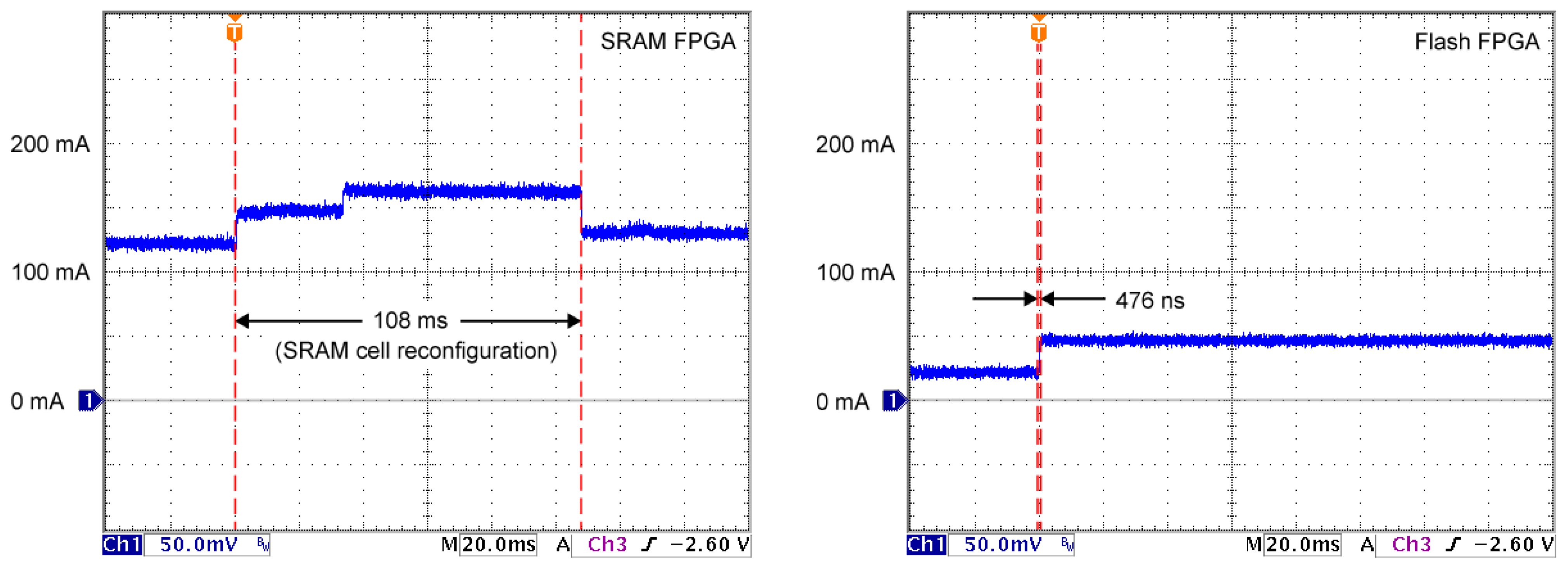
4. Hardware Evaluation

In order to evaluate the Marmote SDR hardware, we created a general development framework along with a prototype baseband application. The framework was designed to be used with various radio front-end modules, including the 2.4 GHz Joshua radio front-end, and to provide valuable insight into the resource usage of the infrastructure components, while the prototype application is meant to serve as a proof-of-concept design for the entire Marmote SDR platform. Such a prototype application also allowed for power consumption comparison with an existing integrated radio chip and a desktop SDR.

4.1. Development Framework

The development framework incorporates the MicroSemi Libero SoC toolchain and a collection of our hardware description language (HDL) and software components. The FPGA fabric contains three main HDL components: the AFE interface, the baseband application skeleton and the MSS interface. The AFE interface utilizes the DDR capable I/O blocks of the FPGA to communicate with the AFE at sample rates up to 22 MHz, both in receive (ADC) and transmit (DAC) modes. The FPGA fabric part of the application skeleton may host only parts of the PHY layer, shifting most of the computational burden onto the microcontroller, or it may incorporate the radio stack up to the MAC level, relieving the Cortex-M3 processor. In either case, the MSS interface uses the AMBA APB bus to transfer data between the FPGA fabric and the ARM Cortex-M3, and serves as a gateway between the application-specific HDL and software components. The MSS software components primarily control the radio front-end and manage the higher-levels of the radio stack. The current framework provides firmware to initialize and control the RF transceiver chip via I/O pins and a MSS SPI peripheral and to communicate with the FPGA in the form of simple register read and write operations, interrupt requests and optional direct memory access transfers.

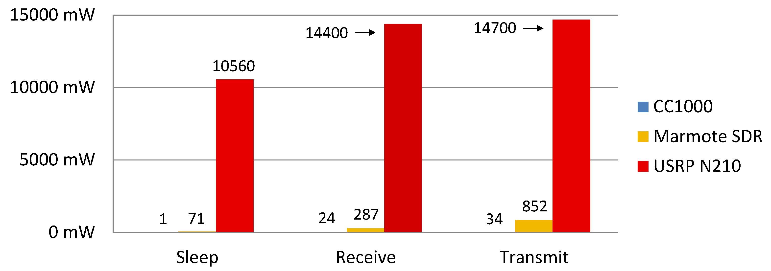
4.2. Power Consumption

In order to evaluate the resource usage of a simple radio transceiver application and the power consumption of the Marmote SDR platform in various power modes, we implemented a simple PHY layer using the above described framework. We chose binary FSK modulation to compare with the representative CC1000 [4] commodity radio used by the MICA2 and TelosB WSN nodes. The FSK modem-based PHY layer has been implemented in the flash FPGA fabric with software-driven control functions running on the MSS. Thus, the analysis of such reference design gives valuable insight into how the flash FPGA logic resources get utilized for PHY layers of similar complexity.
Table 1 summarizes the logic allocation for the FSK modem, along with the interface HDL components. The entire prototype design utilizes 29.5% of the SmartFusion A2F500 logic resources with the APB and AFE interfaces, representing the infrastructure part of the FPGA design, using 12.7% and 0.5%, respectively. The resource requirement of the AFE interface is the same in every application, but that of the APB interface varies highly (4%–15%) based on the amount of registers defined on the APB bus. Thus, in general, it leaves 85%–95% of the FPGA fabric for the user application. Our prototype FSK baseband application takes 16.3% in total, indicating that the total amount of FPGA logic resources allows for experimentation with modulation and demodulation techniques of significantly higher complexity.
Table 1. FPGA logic resource utilization.
ComponentLogic Utilization
APB interface1,469 (12.7%)
AFE interface52 (0.5%)
FSK application1,882 (16.3%)
Total3,403 (29.5%)
To fully characterize the power consumption of the Marmote SDR platform, its current draw is compared to two fundamentally different radio transceiver solutions. The CC1000 is a highly-integrated, low-cost, low-power commodity RF transceiver chip using FSK modulation in the 433 MHz band. The power consumption for the CC1000 was calculated based on the datasheet specifications assuming 3.3 V supply voltage. The other reference for comparison is the USRP N210 [9] mid-price SDR, which offers full-stack design flexibility at a higher price and power consumption. (Note that the power consumption of the embedded series USRP platform, the E100, is actually higher than that of the N210, according to their datasheet.) The latter was calculated based on the measured total current draw of the USRP at 6 V with an SBX daughterboard attached to it. Thus, this value does not include the consumption of the desktop computer that is additionally required for the operation. The Marmote SDR power consumption was measured by the Yellowstone power supply monitor and included the consumption of the Joshua radio front-end and the Teton mixed-signal processing board, with the SmartFusion MSS, FPGA fabric and the AFE running at 10 MHz. (Note that unlike desktop SDR platforms, the Marmote SDR operation does not require a desktop computer.)
Figure 3. Power consumption comparison of the CC1000 commodity radio-frequency (RF) chip, the Marmote SDR platform and the USRP N210 in various power modes.
Jsan 02 00631 g003
The power consumption of the three approaches are compared in Figure 3 in three common scenarios in WSN duty cycle operation: sleep, transmit and receive mode. As WSN nodes usually spend most of their time dormant; sleep mode is expected to reduce current draw to a fraction of that of active modes. The CC1000 offers true sleep mode with power consumption less than 1 mW, the Marmote SDR consumes 70.8 mW, while the USRP N210 does not provide similar low-power feature. In-depth analysis of the Marmote SDR sleep mode showed that the Teton module is responsible for 72% of the Marmote SDR dissipated 70.8 mW, while the Joshua module for the remaining 28%. During sleep mode, all external peripherals were disabled, making the SmartFusion SoPC the main contributor to the 50 mW consumed. Unfortunately, the current SmartFusion MSS lacks advanced low-power modes that achieve sub-1 mW sleep power without turning the power rails off. Switching the power rails off has the adverse effect of the eSRAM losing its content and, therefore, the application losing its state. As reinitializing the application, saving and restoring its state variables results in significant wake up time penalties, we defined the SmartFusion sleep mode with the integrated AFE and ACE powered off, the FPGA put in reset mode, the required MSS peripherals running on 32 kHz and the Cortex-M3 halted, waiting for interrupt. We found the latter SmartFusion configuration to yield the lowest-power mode from which the system can wake up in only a few clock cycles. While the 50 mW power draw is significantly higher than that of our previous microcontroller plus IGLOO flash FPGA approach [17], we consider it a trade-off for the high-bandwidth, on-chip AMBA APB interface between the MSS and the FPGA fabric. As microcontrollers with ultra-low-power sleep mode already exist and the IGLOO flash FPGAs consume less than 60 μW in Flash*Freeze mode [23], we expect manufacturing technology to lower the static power consumption for next generation flash FPGA-based SoPCs significantly. The Joshua radio front-end had two main components, the MAX2830 transceiver chip and the TCXO during sleep mode measurements. As the RF transceiver chip consumes <1 mA in shutdown mode, the main contributor to the 20 mW power is the TCXO. Even though the current Joshua module always keeps the TCXO on, this was a design decision, and it could be turned off in future versions.
In receive mode, Marmote SDR consumes 287.4 mW, approximately 12-times more power than the CC1000 (24.4 mW) and 50-times less than the USRP N210 (14,400 mW). Out of the 287.4 mW, the Teton board SmartFusion and AFE dissipate approximately 80 mW and 15 mW, while the MAX2830 and the TCXO on the Joshua board, around 172 mW and 20 mW, respectively. Comparing the transmit mode power consumption at 0 dBm nominal transmit power, the Marmote SDR dissipates 851.7 mW, the CC1000, 24-times less (34.3 mW), while the USRP N210, 51-times more (14700 mW). The SmartFusion, AFE and TCXO consume the same as in receive mode, while the MAX2830 transmit section and the integrated power amplifier draw roughly 280 mW and 450 mW, respectively.
Thus, considering a 6,000 mAh 3.7 V Li-Ion battery, the Marmote SDR is able to continuously operate for over 24 h in transmit mode (0 dBm) and to run for over 10 days in sleep mode.

5. Communication Protocol Design

Having discussed the design of the Marmote SDR platform debuting a simple FSK-based PHY layer design in Section 3 and Section 4, this section focuses on the development and evaluation of a more advanced communication protocol PHY layer for WSNs. A fundamental task of the wireless communication in a WSN is to transfer the sensory data from the low-complexity and power-constrained sensor nodes to a resourceful base station. This task has generally been achieved using sensor nodes equipped with highly integrated RF chips and base station nodes of essentially the same architecture, but attached to a laptop or desktop computer. The disadvantage of this approach is that it prescribes the use of a CSMA or TDMA access scheme throughout the network, including the base station vicinity, thus, it fails to take advantage of the increased resources usually available at the base station. However, if the PHY layer between a resourceful base station and the directly connected sensor nodes could be redefined, it would allow for experimentation with other multiple access schemes. One potentially beneficial candidate for WSNs is asynchronous DS-CDMA, which holds the following promises:
  • Collision-free multiple-access scheme that allows for simultaneous packet transmissions and reduced packet losses, due to multiple access interference
  • Asynchronous, contention-free medium access that requires no synchronization (scheduling) between sensor nodes
  • Asymmetric communication link shifts the processing burden from sensor nodes to the base station (simple transmitter and complex receiver architecture)
  • Rejection of narrowband interference and jamming
The Marmote SDR platform provides a means to experiment with novel, full-custom physical layer designs by exploiting the direct access to the baseband signals at the sensor nodes. Therefore, we developed a DS-CDMA-based protocol and evaluated its performance using a measurement setup with multiple wireless sensor nodes and a base station, as depicted in Figure 4. In this setup, the sensor nodes were instances of the Marmote SDR platform and primarily acted as DSSS transmitters with uniquely assigned pseudo-noise (PN) code sequences. The “powerful” base station, on the other hand, was represented by a USRP N210 connected to a desktop computer, which ran a GNU Radio implemented receiver, listened for all the assigned PN code sequences and evaluated the protocol performance.
Figure 4. Measurement setup with four Marmote SDR sensor nodes (transmitters), a USRP N210 and desktop computer base station (receiver).
Jsan 02 00631 g004
The rest of this section presents the design of the spread-spectrum DS-CDMA communication protocol optimized for WSNs, along with its experimental evaluation.

5.1. PHY Layer Description

The design of the proposed DS-CDMA PHY layer involved the definition of a suitable packet frame format and the accompanying spreading and modulation parameters. The corresponding transmitter and receiver architectures are directly affected by these decisions, therefore, their structure is also discussed in this section.

5.1.1. Frame Format

The packet frame format used by the protocol consists of a PHY header and a PHY payload part, as shown in Table 2. The PHY header contains a fixed two-byte synchronization pattern used for obtaining symbol, frame and frequency synchronization. The PHY payload comprises four fields, where the source address identifies the sensor node (the PN-sequence assigned to the sensor node can also be used for identification), the sequence number provides a means to ensure frame sequence integrity, payload data carries the actual payload and CRC 16 allows one to check the integrity of the individual frame.
Table 2. Frame format and field lengths (bytes) used in the experimental protocol.
PHY HeaderPHY Payload
Sync patternSource addressSequence numberPayload dataCRC 16
212152

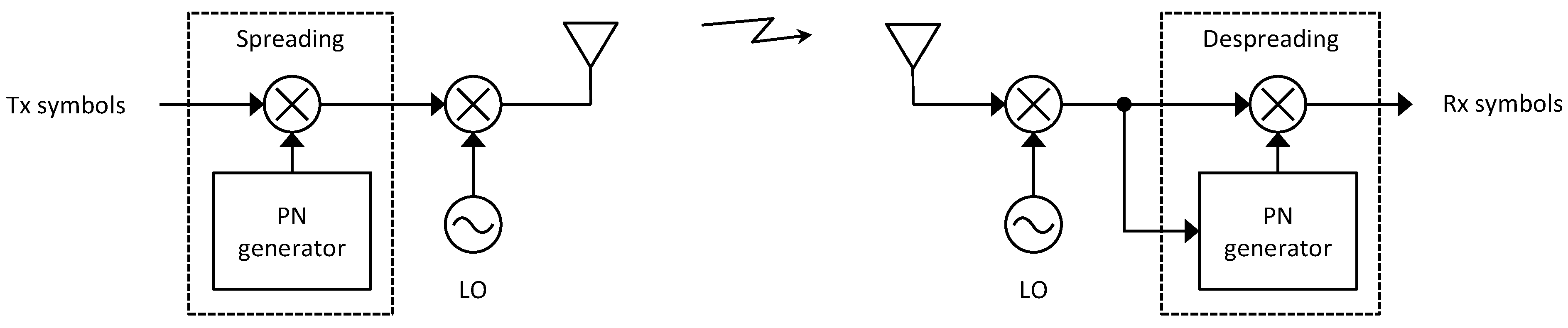
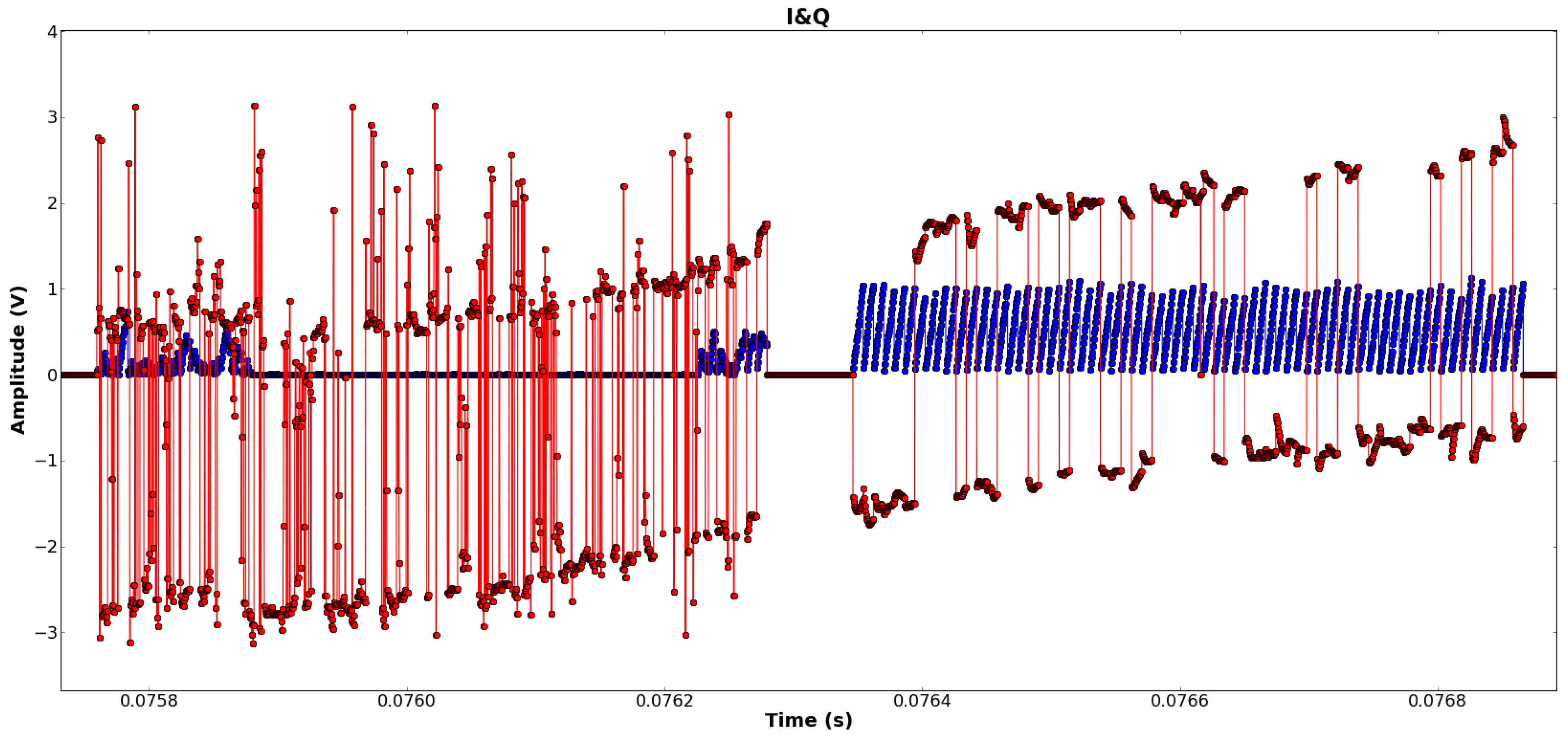
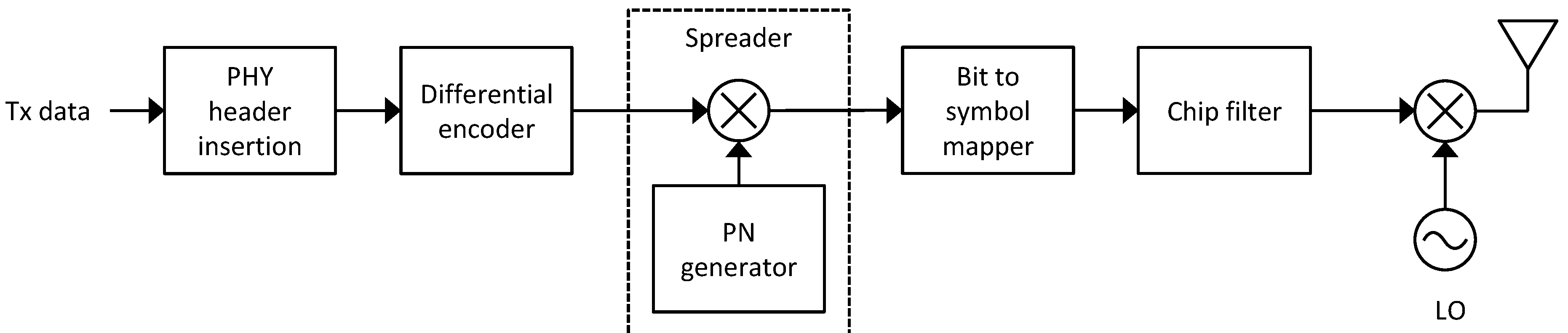
5.1.2. Spreading and Modulation

The proposed communication protocol employs direct-sequence spread spectrum (DSSS) modulation technique, where the transmitted data symbols are multiplied by an independent pseudo-noise (PN) sequence of “chips”, as shown in Figure 5. The spreading PN sequence has a significantly higher chip rate than the original data symbols; therefore, it expands the bandwidth of the original signal accordingly. When the same PN sequence is precisely known and timed at the receiver, its correlation with the received noise-like signal allows for the reconstruction of the original data symbols; see Figure 5. When properly constructed PN-codes are assigned to the sensor nodes, the communication links in the base station vicinity effectively allow for an asynchronous DS-CDMA scheme.
Figure 5. Simplified block diagram of a direct-sequence spread spectrum (DSSS) transceiver.
Jsan 02 00631 g005
In the proposed DS-CDMA protocol, each sensor node is allocated a unique PN spreading sequence, and the same sequences are known a priori at the base station. Two fundamental performance measures of the PN sequences are their auto-correlation and cross-correlation functions. The auto-correlation function is defined as:
R i ( τ ) = - N c T c N c T c PN i ( t ) · PN i ( t - τ ) d t
where N c is the length of the PN sequence and T c is the chip period. The auto-correlation function is expected to have a high correlation peak at τ = 0 and close to zero value at τ 0 , to enable accurate detection of the spread signals. Meanwhile, the cross-correlation function is defined as:
R i , j ( τ ) = - N c T c N c T c PN i ( t ) · PN j ( t - τ ) d t
where N c is the length of the PN sequence and T c is the chip period. R i , j ( τ ) should have close to zero value for any τ, as it measures the agreement between sequences, PN i and PN j , and, consequently, characterizes the possible interference between the two transmitters using these spreading sequences.
PN sequences with outstanding auto-correlation and good cross-correlation properties can be generated using simple linear-feedback shift registers. The class of exactly 2 L - 1 long sequences, which can be produced by L-stage shift registers, are called maximal-length sequences or, simply, m-sequences [24]. The proposed DS-CDMA protocol relies on m-sequences that have a corresponding period of 2 11 - 1 . The nodes are assigned one of the 176 distinct m-sequences to spread the synchronization and data symbols. The PN-generator is reset only at the start of the transmission, as opposed to after each data symbol. Therefore, the transmitter associates a different chip pattern with each symbol, and the receiver follows this same “long-code” approach for PN sequence generation in order to detect and despread the received signal. The binary data symbols are differentially encoded before spreading, and the spread chips are modulated onto the carrier using differential binary phase-shift keying (DBPSK modulation).

5.1.3. Transmitter Design

The DS-CDMA transmitter is associated with a low-complexity architecture that naturally lends itself to the flash FPGA-based SoPC found on the Marmote SDR platform. The MAC-level operations, such as generating the PHY payload and scheduling the transmissions, are handled by the microcontroller, and the assembled PHY payload is transferred to the FPGA fabric through the AMBA bus interface. The PHY-level operations are implemented entirely in the FPGA fabric, as shown in Figure 6. Transmission of a packet starts with prepending the PHY header to the PHY payload and passing the serialized binary data through a differential encoder. The encoded binary data is then spread by the locally synthesized PN sequence. As both the encoded data and the generated PN sequence consist of binary symbols, the multiplication reduces to the inexpensive binary exclusive or (XOR) operation, which is favorable, as the current flash FPGA fabric lacks hardware multipliers. The PN generator is a linear feedback shift register that produces a 2 11 - 1 long m-sequence at a fixed 2 MHz chip rate and features an adjustable generator polynomial and spreading factor. The spread binary symbols are mapped to symbols {- 1 , 1 } and filtered by a root-raised-cosine (RRC) pulse shaping filter before phase modulating the carrier.
Figure 6. Simplified block diagram of the DSSS-based code division multiple access (DS-CDMA) transmitter implemented on the Marmote software-defined radio (SDR) platform.
Jsan 02 00631 g006
The corresponding FPGA resource utilization is coarsely summarized in Table 3. The entire DSSS transmitter path (not including the chip filter) takes approximately 14% of the available resources. The PN generator is responsible for 2% and the differential encoder, XOR multiplier and symbol mapper for less than 2% in total. Thus, similarly as in Section 4.2, the APB bus interface and configuration registers contribute most to the 14.1%. The chip filter, on the other hand, is a 31-tap (finite impulse response) FIR filter synthesized from a high-level design description with 16-bit coefficients. While it consumes 28.4% of the available total FPGA logic resources, the filter is a non-critical element, and its complexity could be greatly reduced without significant performance degradation.
Table 3. FPGA logic resource utilization of the DSSS transmit path.
ComponentLogic Utilization
DSSS transmitter1,624 (14.1%)
Chip filter3,272 (28.4%)
Total4,896 (42.5%)

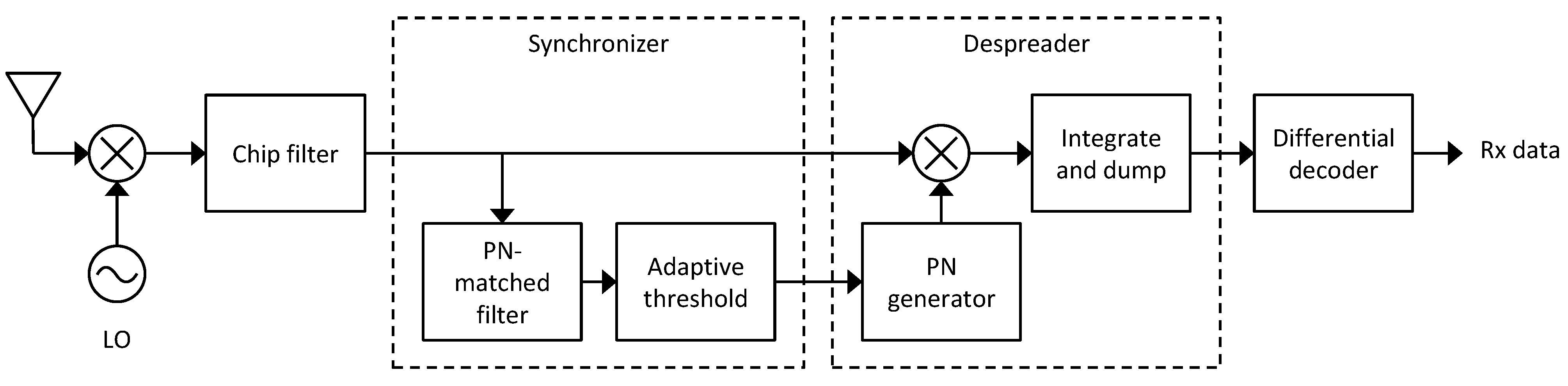
5.1.4. Receiver Design

As the DS-CDMA receiver is of significantly higher complexity than the transmitter, it is implemented in GNU Radio and run on a high-performance desktop computer connected to a USRP N210 radio front-end. The block diagram of the receiver associated with one particular PN code sequence is shown in Figure 7. Note that in a multi-node setup with four unique PN code sequences, the synchronizer, despreader and differential encoder blocks are replicated four times.
Figure 7. Simplified block diagram of the DS-CDMA receiver implemented on the USRP N210 and GNU Radio platform.
Jsan 02 00631 g007
The chip filter is an RRC filter with the same parameters as the pulse shaping filter in the transmitter. Together, the transmit and receive chip filters perform matched filtering to minimize the inter-symbol interference. The filtered samples are fed to the synchronizer block to detect the frame and obtain symbol and frame synchronization. The synchronizer block comprises a PN-matched filter, with coefficients corresponding to the first segment of the spreading sequence and a noise-adaptive peak detector. The PN-matched filter calculates the correlation value at each sample, which gives the shortest acquisition time at the expense of significant computational requirement. (Note that such rapid acquisition is essential in sensor networks, where the packed lengths tend to be short.) According to Equation (1) and (2), the PN-matched filter (correlator) output exhibits peaks when the corresponding PN spread synchronization pattern is found, but remains insensitive for patterns spread by other PN sequences, see Figure 8. The adaptive threshold logic determines the peak indexes and sets the time base for the despreader block to reconstruct the PHY payload from the spread packet.
Figure 8. The output of the PN-matched filter in the synchronizer, showing distinct pulses at the start of five spread packet frames and insensitivity to noise and other ongoing network traffic.
Jsan 02 00631 g008
Figure 9. The amplitude (blue) and phase (red) of the integrate and dump block output for an inaccurately (left) and an accurately (right) synchronized packet.
Jsan 02 00631 g009
The despreader block is essentially a serial correlator, where the PN generator realizes a 2 11 - 1 long m-sequence through a linear-feedback shift register. The PN generator is reset and triggered by the synchronizer block to properly time the onset of the integrate-and-dump block, performing:
I k ( τ ) = k N p T c ( k + 1 ) N p T c r ( t - τ ) · PN i ( t ) d t 0 k < K
where I k ( τ ) is the integrator output for the k th payload symbol, N p is the spreading factor, T c is the chip period, r ( t ) is the complex chip-filtered signal, PN i ( t ) is the despreading PN sequence of the i t h receiver, τ is the assumed onset of the first payload symbol and K is the number of payload symbols. Figure 9 shows that the phase of the integrator output is noise-like when inaccurately synchronized. However, in the case of accurate synchronization, its amplitude steadily builds up and its phase remains stable, allowing for proper non-coherent demodulation in the differential decoder.

5.2. Evaluation

The primary goal of the protocol evaluation was to characterize the PHY layer performance in a real-world scenario. For that, the PHY layer protocol was implemented using Marmote SDR nodes and an USRP N210/GNU Radio base station. The configured nodes were deployed in an office environment, and the packet reception ratio was registered under varying traffic load, using a different number of nodes and different spreading factors.

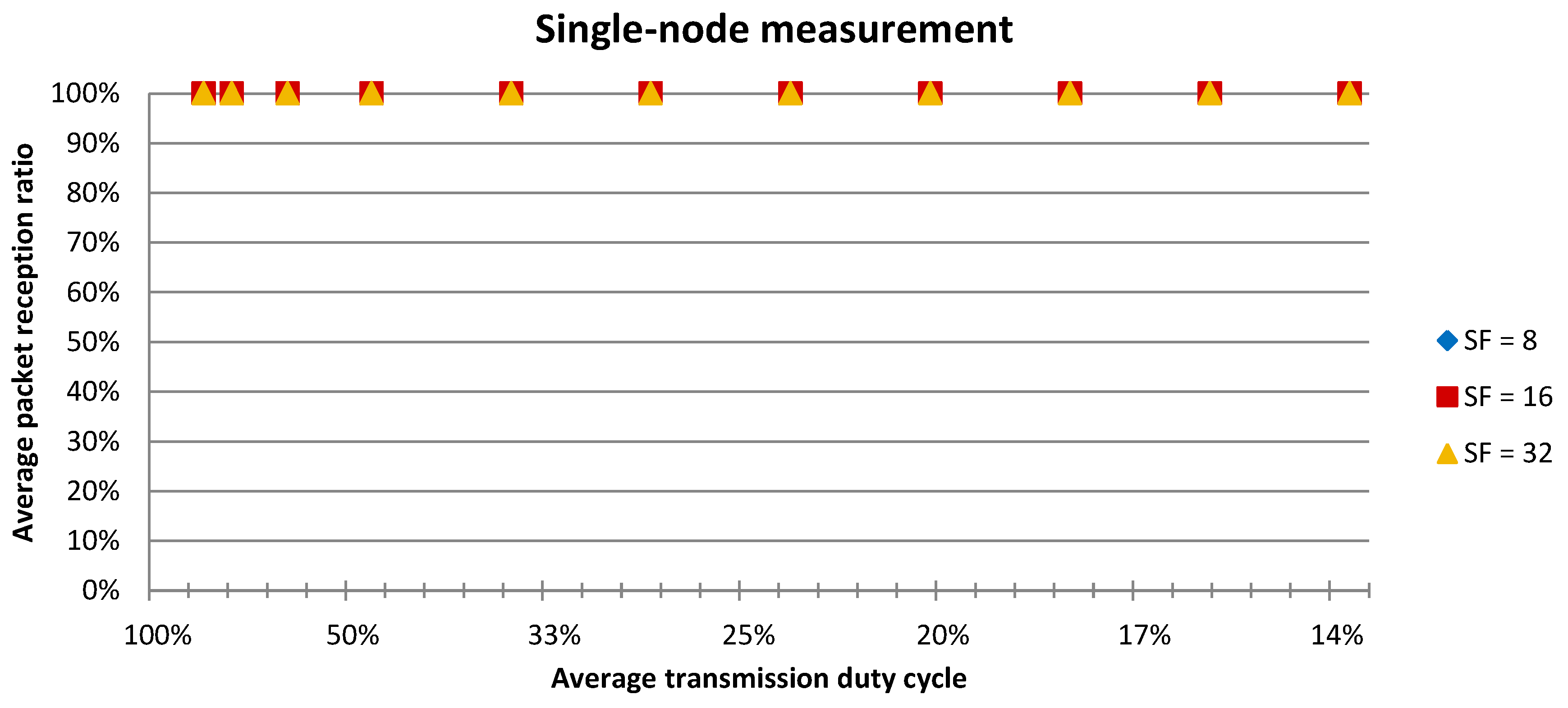
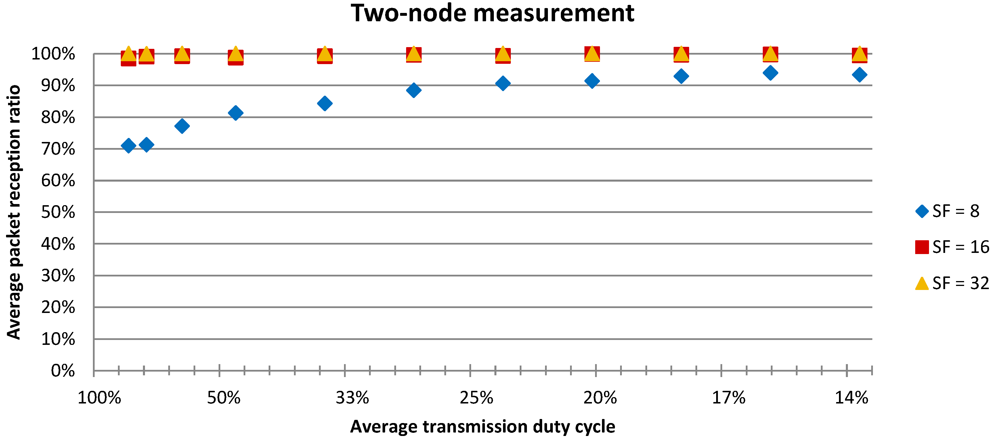
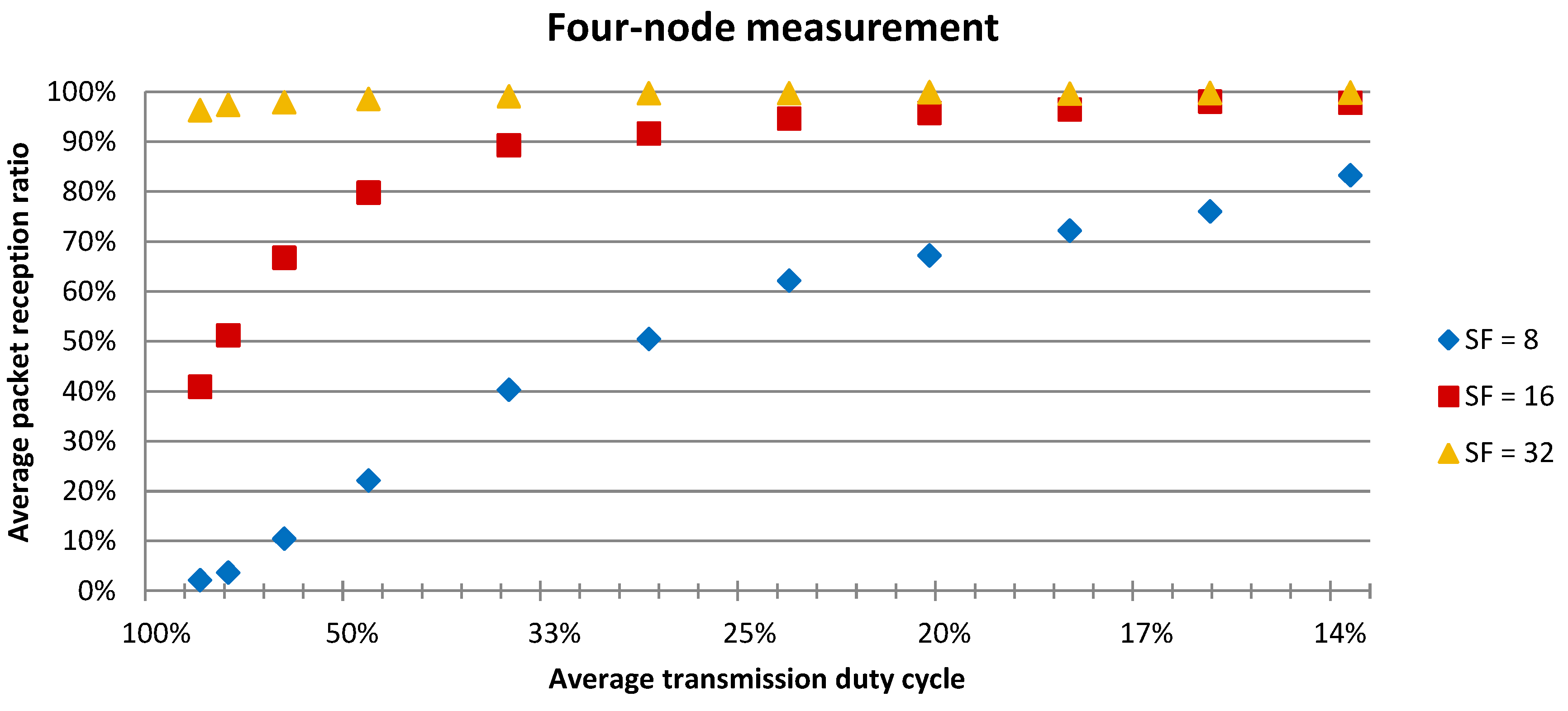
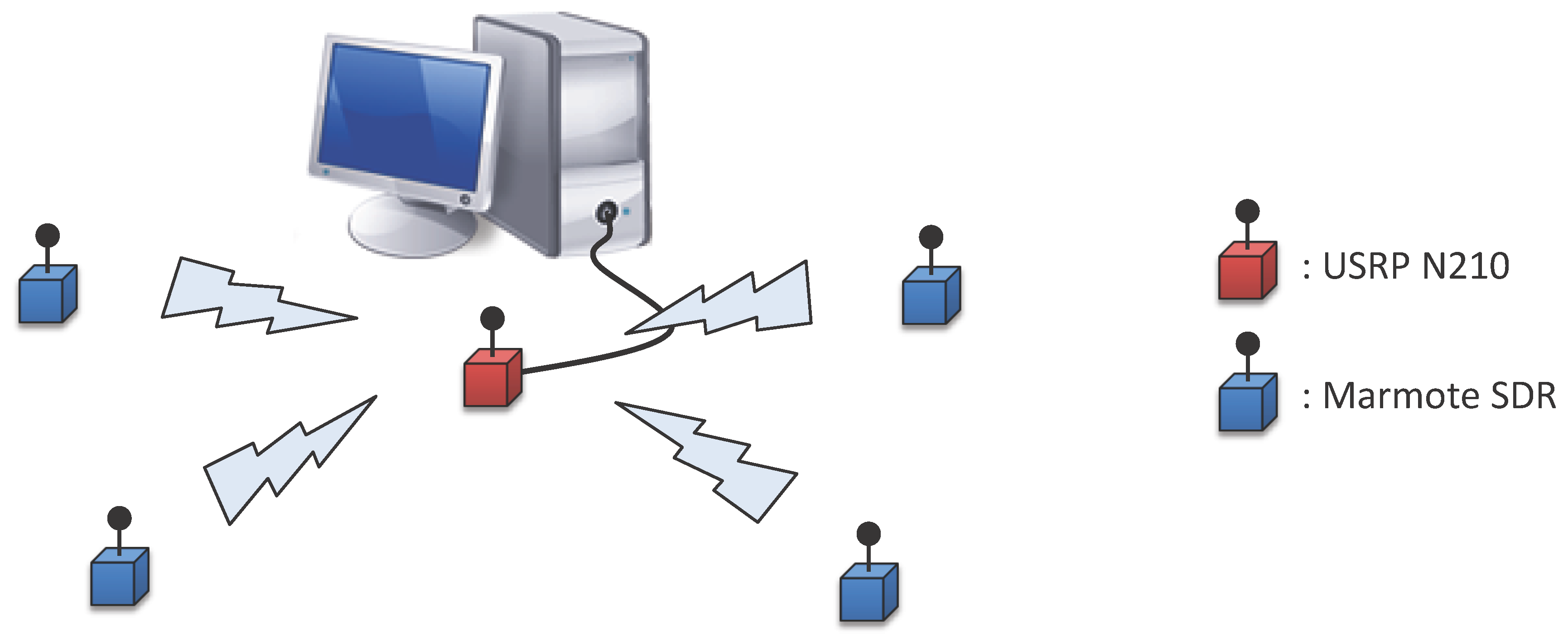
5.2.1. Experiment Setup
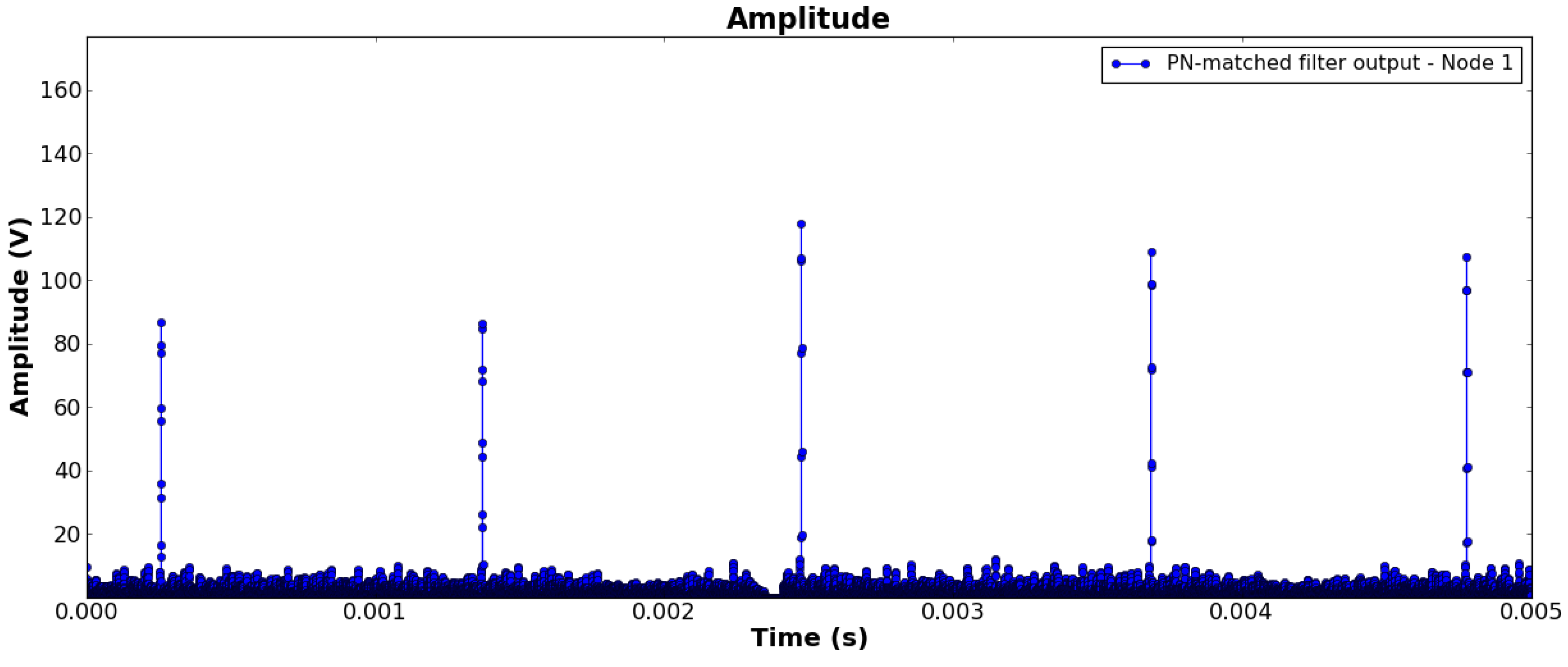
The three measurements scenarios involved 1, 2 or 4 Marmote SDR nodes and a USRP/GNU Radio base station deployed in an office environment; the four-node setup is shown in Figure 4. The radios were tuned to 2.405 GHz, with the nodes continuously transmitting packets and the base station evaluating the average packet reception ratio based on 1,000 transmitted packets. The packets frames were constructed on the Marmote SDR nodes based on the format described in Section 5.1.1, each carrying a payload of 20 bytes. To control the traffic load, the packet transmission was initiated periodically with a predefined average τ avg interval having 20% jitter. That is, the interval between two consecutive packet transmission was calculated according to:
Δ τ = τ avg ( 1 + 0 . 2 · U - 1 , 1 )
where U · denotes the uniform distribution. The chip rate was fixed at 2 MHz for all cases; therefore, the spreading factor values 8, 16 and 32 reduced the data rate to 250 kbps, 125 kbps and 62.5 kbps, respectively.
The GNU Radio-implemented receiver, run on an USRP N210 connected to a desktop computer, listened for all sensor nodes and kept track of the packet reception ratio (PRR) for each based on the received sequence number and CRC 16 fields. For each measurement, the receiver spreading factor was set manually to match that of the transmitters, while the power control was adjusted based on the perceived PRR.

5.2.2. Results

The single-node measurement was used to create a baseline with interference coming from the environment only. The results plotted in Figure 10 show that a reliable communication link was established independently of the spreading factor used. The packet delivery ratio was 100%, regardless of the traffic load, as one would expect for a contention-free and clear channel.
Figure 10. Packet reception ratio for the single-node setup under various traffic loads with spreading factors of 8, 16 and 32.
Jsan 02 00631 g010
The two-node measurement introduces multiple access interference (MAI) to the channel, as shown in Figure 11, which clearly impacts the packet delivery ratio for the low processing gain case. Under heavy traffic conditions, the average packet delivery ratio dropped to 71% for a spreading factor of 8 and to 99% for that of 16. Examination of the received data showed that packet losses were equally probable due to missed detection of the synchronization header and to the corruption of the payload data.
Figure 11. Packet reception ratio for the two-node setup under various traffic loads with spreading factors of 8, 16 and 32.
Jsan 02 00631 g011
The four-node setup further increased the MAI in the channel, creating a more realistic multi-node scenario. The observed average packet delivery ratios depicted in Figure 12 show that with a spreading factor of 8, more than 16% of the packets were dropped in a low-traffic channel, approximately 50% were lost under moderate traffic and only 2% were delivered in high traffic. Increasing the processing gain to 16 improved the average packet reception ratio to over 90% in moderate network traffic, but it falls down to 41% under heavy loads. Meanwhile, increasing the spreading factor to 32, the protocol delivers over 96% of the packets on average, even in a highly loaded channel.
Figure 12. Packet reception ratio for the four-node setup under various traffic loads with spreading factors of 8, 16 and 32.
Jsan 02 00631 g012
In summary, our experiments showed that the designed DSSS communication protocol performs reliably when there is no contention in the channel. A processing gain of 8 already offered reasonable protection against external interferences, such as the ongoing WLAN communication; however, as the number of nodes increased, such a low degree of spreading offered little protection against simultaneous transmission, even under low traffic loads. Therefore, a truly collision-free DS-CDMA communication calls for reasonable spreading factors, which still remains a design parameter, primarily determined by the size of the network and the expected network traffic. A detailed performance analysis with respect to these network parameters is given in [25]. In the presented experimental setup, the desired processing gain was attained by using a fixed chip rate and reducing the effective data rate. Alternatively, the data rate could be fixed, and the chip rate could be increased to achieve the same goal, without increasing the transmitter complexity.

6. Conclusions

Long-term deployed WSN nodes face ultra-low-power requirements that have been combated on several fronts in the past decade. Power consumption of computational resources has been rapidly reduced through advances in semiconductor process technology, but the same does not hold for the radio communication interface. Significant energy may be saved related to wireless communication in WSNs through the design of full-vertical communication protocol stacks tailored for the specific WSN application. Traditional WSN nodes utilize highly integrated off-the-shelf radio transceiver chips that implement the lower layers in ASIC and, therefore, reduce the design flexibility of those layers. SDRs, on the other hand, give full access to the entire stack and allow for rapid prototyping, but their power consumption is prohibitively large for practical battery-based operation.
In this paper, we presented the hardware design of the Marmote SDR platform, an experimental research platform for WSN communication stacks. Through the flash FPGA-based SoPC architecture, the platform allows for rapid and flexible design of full network stacks from baseband processing in the PHY up to the application layer, which is not possible with integrated radio chips. The computational resources offered by Marmote SDR are less than, but comparable to, that of desktop-connected SDRs. In return, the Marmote SDR consumes an order of magnitude less power than a desktop SDR, although still significantly more than an integrated RF transceiver. The power consumption of Marmote SDR with the Joshua 2.4 GHz radio front-end is approximately 0.25 W in receive and 0.8–1.5 W in transmit mode, depending on the transmit power. This allows for several hours-long battery based operation, which can be further extended by duty cycling. Deployment of a Marmote SDR WSN with a prototype network stack enables researchers to collect real world data on the communication protocol performance, rather than relying solely on simulation results—often prone to oversimplification. An experimentally-verified protocol stack can then be implemented as a highly integrated transceiver, resulting in a much smaller size and a significantly smaller power budget. We believe that a platform like Marmote SDR can serve as a springboard for many novel low-power transceiver solutions in the future.
The hardware, HDL and software design files of the Marmote SDR platform are open-source and freely available for download from [26].

Acknowledgments

This material is based upon work supported by the National Science Foundation under Grants No. 0964592 and No. 1035627.

Conflicts of Interest

The authors declare no conflict of interest.

References

  1. Crossbow. Crossbow MICAz (MPR2400) Radio Module. Available online: http://www.xbow.com (accessed on 1 June 2013).
  2. Polastre, J.; Szewczyk, R.; Culler, D. Telos: Enabling Ultra-Low Power Wireless Research. In Proceedings of the Fourth International Symposium on Information Processing in Sensor Networks (IPSN 2005), Los Angeles, CA, USA, 15 April 2005.
  3. Bachir, A.; Dohler, M.; Watteyne, T.; Leung, K.K. MAC essentials for wireless sensor networks. IEEE Commun. Surv. Tutor. 2010, 12, 222–248. [Google Scholar] [CrossRef]
  4. Texas Instruments. Chipcon AS, CC1000: Single Chip very Low Power RF transceiver. 2004. Available online: www.ti.com/lit/ds/symlink/cc1000.pdf (accessed on 1 June 2013).
  5. Texas Instruments. CC2420: 2.4 GHz IEEE 802.15.4 / ZigBee-Ready RF Transceiver. 2007. Available online: http://www.ti.com/lit/ds/symlink/cc2420.pdf (accessed on 1 June 2013).
  6. Ali, M.; Saif, U.; Dunkels, A.; Voigt, T.; Römer, K.; Langendoen, K.; Polastre, J.; Uzmi, Z.A. Medium access control issues in sensor networks. Comput. Commun. Rev. 2006, 36, 33–36. [Google Scholar] [CrossRef]
  7. Neufeld, M.; Fifield, J.; Doerr, C.; Sheth, A.; Grunwald, D. SoftMAC—Flexible Wireless Research Platform. In Proceedings of the Fourth Workshop on Hot Topics in Networks HotNetsIV, College Park, MD, USA, 14 November 2005.
  8. Blossom, E. GNU radio: Tools for exploring the radio frequency spectrum. Linux J. 2004, June 2004(122), 4. [Google Scholar]
  9. Ettus Research. USRP N210. Available online: https://www.ettus.com/product/details/UN210-KIT (accessed on 1 June 2013).
  10. Xilinx Inc. Xilinx System Generator for DSP. Available online: http://www.xilinx.com/tools/sysgen.htm (accessed on 1 June 2013).
  11. Ahola, T.; Korpinen, P.; Rakkola, J.; Ramo, T.; Salminen, J.; Savolainen, J. Wearable FPGA Based Wireless Sensor Platform. In Proceedings of the 29th Annual International Conference of the IEEE Engineering in Medicine and Biology Society (EMBS 2007), Lyon, France, 23–26 August 2007; pp. 2288–2291.
  12. Hayek, A.; Machmur, B.; Suna, Y.; Borcsok, J. FPGA-Based Wireless Sensor Network Platform for Safety Systems. In Proceedings of the IEEE 19th International Conference on Telecommunications (ICT), Jounieh, Lebanon, 23–25 April 2012; pp. 1–6.
  13. Völgyesi, P.; Balogh, G.; Nádas, A.; Nash, C.; Lédeczi, A. Shooter Localization and Weapon Classification with Soldier-Wearable Networked Sensors. In Proceedings of the 5th International Conference on Mobile Systems, Applications, and Services (MobiSys), San Juan, Puerto Rico, 11–14 June 2007.
  14. Valverde, J.; Otero, A.; Lopez, M.; Portilla, J.; de la Torre, E.; Riesgo, T. Using SRAM based FPGAs for power-aware high performance wireless sensor networks. Sensors 2012, 12, 2667–2692. [Google Scholar] [CrossRef] [PubMed]
  15. SDR4All. Flexible Radio Platform. Available online: http://www.flexible-radio.com/sdr4all (accessed on 1 June 2013).
  16. OSmoSDR. OsmoSDR Project. Available online: http://sdr.osmocom.org (accessed on 1 June 2013).
  17. Ledeczi, A.; Hay, T.; Volgyesi, P.; Hay, D.; Nadas, A.; Jayaraman, S. Wireless acoustic emission sensor network for structural monitoring. IEEE Sens. J. 2009, 9, 1370–1377. [Google Scholar] [CrossRef]
  18. Nylanden, T.; Janhunen, J.; Hannuksela, J.; Silven, O. FPGA Based Application Specific Processing for Sensor Nodes. In Proceedings of the IEEE 2011 International Conference on Embedded Computer Systems: Architectures, Modeling and Simulation, Samos, Greece, 18–21 July 2011; pp. 118–123.
  19. Philipp, F.; Glesner, M. Mechanisms and Architecture for the Dynamic Reconfiguration of an Advanced Wireless Sensor Node. In Proceedings of the 2011 International Conference on Field Programmable Logic and Applications (FPL), Crete, Greece, 5–7 September 2011; pp. 396–398.
  20. Kuo, Y.S.; Pannuto, P.; Schmid, T.; Dutta, P. Reconfiguring the Software Radio to Improve Power, Price, and Portability. In Proceedings of the 10th ACM Conference on Embedded Networked Sensor Systems (Sensys’12), Toronto, ON, Canada, 6–9 November 2012.
  21. Szilvási, S.; Sallai, J.; Amundson, I.; Völgyesi, P.; Lédeczi, Á. Configurable Hardware-based Radio Interferometric Node Localization. In Proceedings of the 2010 IEEE Aerospace Conference, Big Sky, MT, USA, 6–13 March 2010.
  22. Microsemi. Total System Power. Available online: http://www.actel.com/documents/Power_PIB.pdf (accessed on 1 June 2013).
  23. Microsemi. IGLOO Low Power Flash FPGAs with Flash*Freeze Technology. Available online: http://www.actel.com/documents/IGLOO_DS.pdf (accessed on 1 June 2013).
  24. Simon, M.K.; Omura, J.K.; Sholtz, R.A.; Levitt, B.K. Spread Spectrum Communications Handbook; Electronic communications, McGraw-Hill Professional Publishing: New York, NY, USA, 1994; pp. 283–284. [Google Scholar]
  25. Geraniotis, E. Performance of noncoherent direct-sequence spread-spectrum multiple-access communications. IEEE J. Sel. Areas Commun. 1985, 3, 687–694. [Google Scholar] [CrossRef]
  26. Marmote SDR Platform. Marmote low-power FPGA-based platform. Available online: http://marmote.googlecode.com (accessed on 1 June 2013).

