Article

Physical Layer Design in Wireless Sensor Networks for Fading Mitigation

ECE Department, The University of Auckland, 38 Princes Street, Auckland 1010, New Zealand
*
Author to whom correspondence should be addressed.
J. Sens. Actuator Netw. 2013, 2(3), 614-630; https://doi.org/10.3390/jsan2030614
Submission received: 26 June 2013 / Revised: 12 August 2013 / Accepted: 19 August 2013 / Published: 2 September 2013
(This article belongs to the Special Issue Feature Papers)

Abstract

:
This paper presents the theoretical analysis, simulation results and suggests design in digital technology of a physical layer for wireless sensor networks. The proposed design is able to mitigate fading inside communication channel. To mitigate fading the chip interleaving technique is proposed. For the proposed theoretical model of physical layer, a rigorous mathematical analysis is conducted, where all signals are presented and processed in discrete time domain form which is suitable for further direct processing necessary for devices design in digital technology. Three different channels are used to investigate characteristics of the physical layer: additive white Gaussian noise channel (AWGN), AWG noise and flat fading channel and AWG noise and flat fading channel with interleaver and deinterleaver blocks in the receiver and transmitter respectively. Firstly, the mathematical model of communication system representing physical layer is developed based on the discrete time domain signal representation and processing. In the existing theory, these signals and their processing are represented in continuous time form, which is not suitable for direct implementation in digital technology. Secondly, the expressions for the probability of chip, symbol and bit error are derived. Thirdly, the communication system simulators are developed in MATLAB. The simulation results confirmed theoretical findings.

1. Introduction

Wireless sensor networks based on IEEE Standard 802.15.4 [1] can be considered as an emerging technology that will be widely used in this century. Due to the expected autonomous operation of these networks, one of the main demands on the networks and their components design is to have low-power consumption. This power consumption can be reduced by constructing low-power sensor nodes and by the design of such protocols in the network that will reduce this consumption. In this paper the physical layer design is proposed, based on the chip interleaving technique, which can reduce power consumption in the network.
There are not too many references talking exclusively about physical layer design. A paper related to the modulator and demodulator design is presented in [2]. The whole transceiver design is presented in [3]. Paper [4] presents possibility of using OFDM in wireless sensor networks for underwater communications. In [5] a low power cooperative multiple inputs multiple output scheme with low density parity check channel codes is proposed for an adaptive fault tolerant systems. Some issues related to the physical layer performance estimation are presented in [6], which is not targeted to the design but to the problems of position estimation.
The processing in the physical layer includes techniques applied in direct sequence spread spectrum (DSSS) systems and code division multiple access systems (CDMA). It was shown that the chip interleaving techniques can reduce the influence of fading in DSSS and CDMA systems [7,8,9,10]. Following this finding, it was also shown that the chaotic sequences can be used in these systems, which increases security in signal transmission [9] when appropriate sequence synchronization is achieved [11,12]. Following these findings this paper is proposing theoretical model of a communication system representing physical layer of wireless sensor networks. The system is analyzed for two basic cases. First case, when a single-correlator receiver is used for a binary signal transmission and the second case when an N-correlator receiver is used for symbol transmission. The spreading sequences used are defined by the Standard [1].
The contributions of this paper are as follows. Firstly, the mathematical model of communication system representing physical layer is based on the discrete time domain signal representation and processing. In the existing theory, these signals and their processing are represented in continuous time form. However, signals in analog form are not suitable for direct implementation of the system mathematical model into digital technology; thus, all signals in this paper are represented in discrete time form. Secondly, in contrast to published work in [2,3], where the signals are analyzed in analog form and theoretical expressions for the BER are not derived, in this paper the exact theoretical analysis was performed and the expressions for probability of chip, symbol and bit error are derived for the case of noise, fading and interleaver presence inside communication system. According to the authors’ knowledge, these expressions have not been derived yet in the closed form as it was done in this paper. In addition, the derivative of theoretical expressions for the system with interleavers makes a particular contribution of this paper. Thirdly, simulators are developed in MATLAB and simulation results confirmed theoretical findings. These simulators included transceiver simulation according to the Standard [1] and channel simulation. The channel simulator generated and controlled the noise power and fading in discrete time domain. The discrete time domain theoretical model and discrete time domain simulators design allowed direct implementation of the system in DSP technology. Namely, it is quite simple to develop programs in, say, C language for DSP design having confirmed the system operation by simulation in MATLAB. In contrast to work presented in [2], where BER characteristics were given only for developed prototypes, this paper allows comparison of theoretically expected results and results of simulation. Also, the system developed in this paper allows easy changes in the system structure and further analysis of the other possible options in the system design.
The paper contains six Sections starting with this Introduction. In the second Section a theoretical structure of the system is presented and procedure of signal processing in each block is demonstrated when AWG noise is present in the channel. The complete analysis is done for a single-correlator and N-correlator receiver. Section 3 presents the behavior of the system in presence of fading. The interleaver and deinterleaver structure can mitigate the fading in the system. The theoretical model of the system and derivation for the bit error rate expressions for this case are presented in Section 4. The system is simulated for all cases analyzed in previous theoretical sections and simulation results are presented in Section 5. Conclusions of the paper are contained in Section 6.

2. Theoretical Model of a System in the Presence of Gaussian Noise

Figure 1 presents the block scheme of a communication system for physical layer using Offset Quadrature Phase Shift Keying (OQPSK) modulation and spreading of the signals as used in wireless sensor networks. When only Gaussian noise is present in the channel the fading coefficient is set to be one, i.e., α = 1. In order to develop theoretical model of the whole system with N correlators, the analysis will start with the case when the symbols are generating at the source output in binary form and detected at the receiver side using one correlator. Generally, for the system with N-correlators, the source generates message bits which are converted into symbols bjn(k). To each symbol a spreading sequences cin(k) is assigned to obtain a chip sequence m(k) = bjn(k)cin(k) that comes to the input of a multiplexer. If a symbol is in binary form, bjn(k) = ±1, then the system represents a direct sequence spread spectrum system (DSSSS) and the receiver has one correlator as it was said before. If a combination of K bits represents a symbol then the number of sequences sent is N = 2K, which is equal to the number of required correlators at the receiver side. Thus, in the following sections, two cases, a single and N-correlator receiver, will be analyzed.

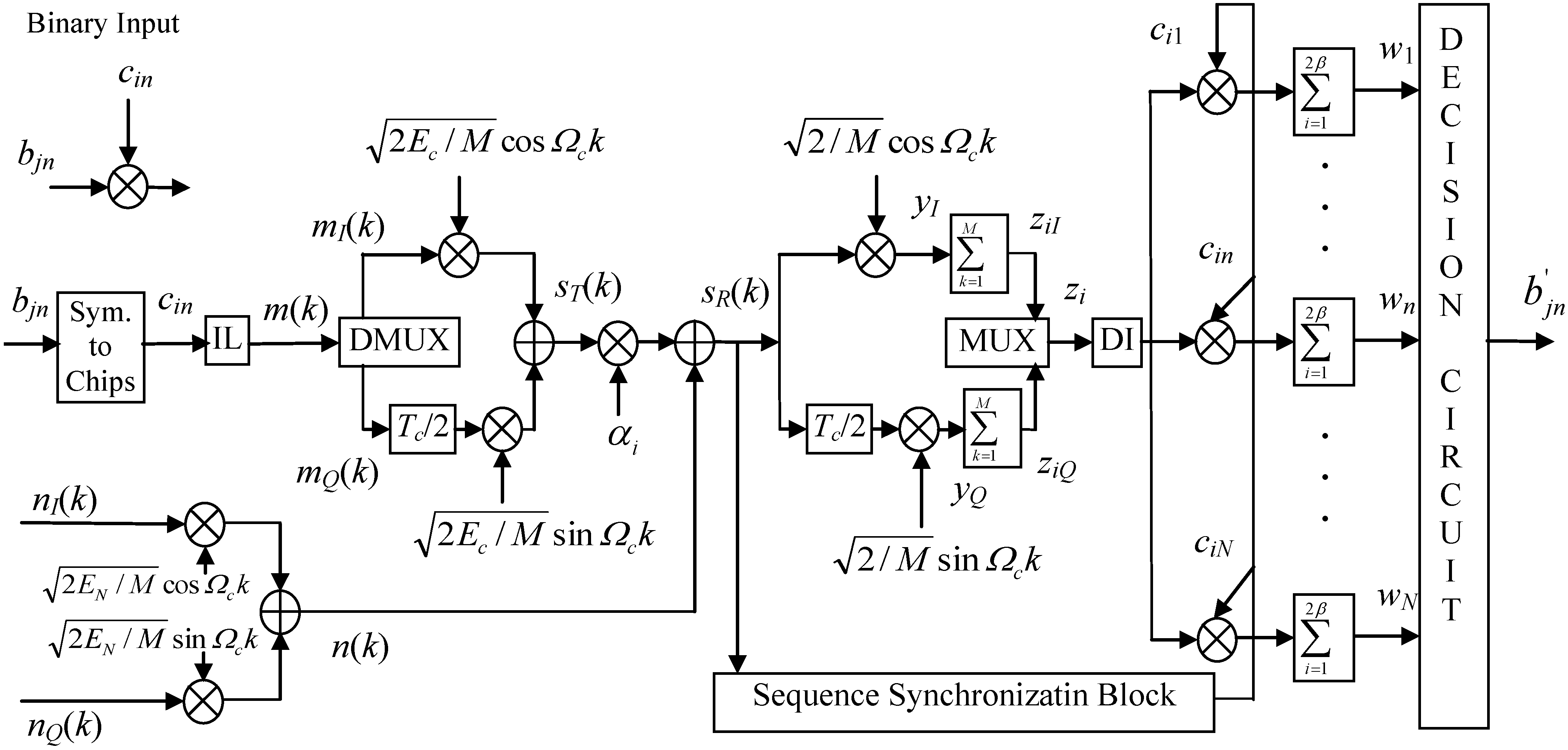
2.1. Single-Correlator Receiver

In this case the spreader is represented by a multiplier, as shown on the left hand upper side of Figure 1, and a single correlator with output w1 at the receiver side. The chip sequence m(k) is split into in-phase and quadrature sequences using the demultiplexer block (DEMUX) in such a way that the even-indexed chip sequence mI(k) modulates the in-phase carrier Jsan 02 00614 i001 and odd-indexed chip sequence mQ(k) modulates the quadrature carrier Jsan 02 00614 i002, where Ec is the energy per chip and M is the number of interpolated samples contained in one chip interval. Therefore, the transmitted signal can be defined as
Jsan 02 00614 i003
where mI(k) and mQ(k) are in-phase and quadrature chip sequences expressed in discrete time domain respectively and c is the frequency of the carrier. It is important to note that k is a discrete time variable.
The noise is to be generated at discrete time instants defined by k. Thus, the band-limited pass-band noise is expressed as
Jsan 02 00614 i004
where the energy of the noise samples inside a chip interval is EN =N0/2 and nI and nQ are in-phase and quadrature noise samples of zero mean and unit variance. The block schematic of this noise generator is presented inside Figure 1. The noise is expressed in this form to comply with the applied signal processing demodulation procedure of both the signal and noise at the receiver side. Namely, in simulation, it is important to achieve that the power of the noise in respect to the power of the signals are controlled at all times at the transmitter side.
Figure 1. Block schematic of communication system.
Jsan 02 00614 g001
The received noisy signal sR(k)= s(k) = n(k) is demodulated using a correlator that consists of a multiplier and an adder. It is sufficient to present the processing of the signal in one branch of the demodulator because the processing in both branches is equivalent. The signal at output of the receiver multiplier is
Jsan 02 00614 i005
The samples of this signal are added in the chip interval (corresponds to integration in continuous time systems). Because, in the case of a single-correlator receiver, the source generates binary signal the output of the transmitting spreader was the first spreading sequence ci1(k), i.e., m(k) = ci1(k), and a random sample zi of a random process Zi in I branch is obtained, i.e.,
Jsan 02 00614 i006
and in Q branch as
Jsan 02 00614 i007
A multiplexer (MUX) is used to combine in-phase and quadrature sequences back into a 2β-chip sequence zi
Jsan 02 00614 i008
where ni are samples of the in-phase and quadrature baseband noise having zero mean and unit variance. In the correlator block, a locally generated reference chip sequences (ci1, i 1,2,3,...,2β) is multiplied with the incoming zi random sequence and then the products are added inside the bit interval. The resulting sum for the first positive message bit sent is
Jsan 02 00614 i009
This value is a random sample of a random variable defined for the first bit received. If the source generates binary bits from the alphabet ±1, the threshold value in the decision circuit needs to be set to zero, and the optimum decision need to be made according to this rule
Jsan 02 00614 i010
Due to the central limit theorem (CLT) the random variable w1 can be approximated by the Gaussian random variable, with its mean
Jsan 02 00614 i011
Due to the statistical independence of the noise and the spreading sequence the second term in Equation (9) is zero. Assuming that the powers of all chips are identical and equal to Pc, we may have
Jsan 02 00614 i012
The related variance is
Jsan 02 00614 i013
Due to the statistical independence of noise variables, the second term is zero. The first and third terms are
Jsan 02 00614 i014
The powers for all chips are equal and the power of noise is equal to the noise variance. Therefore, the variance of w1 can be expressed in this general form
Jsan 02 00614 i015
According to the CLT the density function of variable w1 is Gaussian and can be expressed as
Jsan 02 00614 i016
Then, the probability of error can be calculated according to this expression
Jsan 02 00614 i017
By inserting Equations (10) and (13) into (14) we may find the expression for the probability of bit error in this closed form
Jsan 02 00614 i018
which can be simplified to
Jsan 02 00614 i019
where expressionΨ = Jsan 02 00614 i020 
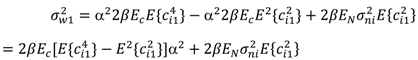
represents random variability of the spreading sequence. The energy of the noise is equivalent to the power spectral density of the two sided noise spectrum. As it was said before, this system is analyzed assuming that the signals are generated in discrete time domain. Each chip and related noise sample are generated once for each chip interval and then repeated (interpolated) M times in that chip interval to allow the discrete time carrier modulation. For M repeated samples of noise in a chip interval the energy is EN = Mσ2. For variance σ2 = BN0 and the bandwidth B=1/2Tc=1/2M, the energy is calculated to be EN = N0/2. If the source generates binary bits and the spreading sequence is in binary form, we may have
Jsan 02 00614 i021
where the energy of a bit is related to the energy of a chip as Eb = 2βEc.

2.2. N-Correlator Receiver

In this case, the source can generate K-bit symbols [1]. Thus, the number of required sequences will be N = 2K. The modulation and demodulation will be the same as in the case of a single-correlator receiver. However, the correlation for each sequence must be performed in its own receiver correlator. Therefore, at the receiver, a bank of N correlators needs to be implemented, as shown in Figure 1.
The receiver for binary symbols transmission is analyzed in previous section. In that case it was sufficient to have the first correlator in the receiver and the symbol to sequence conversion is performed by a multiplier as shown separately in Figure 1. For that case the random variable w1 at the output of the first correlator is calculated in Equation (7) and the related mean, variance and probability of error in Equations (9), (12) and (16).
If the source generates N symbols, which correspond to combinations of message bits, the receiver will use all N correlators in Figure 1. The decision circuit now is a comparator of correlator outputs. The order of these outputs corresponds to the order of the spreading sequences that could be sent at the transmitter side. The decision circuit decides according to this decision rule: the sequence/symbol received corresponds to the maximum output value of the decision circuit. This, if the maximum is at the output three the decision sequence will say the third symbol was sent.
Suppose that the first sequence is sent. Following the procedure of a single-correlator receiver modeling, the output of the n-th correlator can be expressed as
Jsan 02 00614 i022
The first term is inter-sequence interference and the second term is noise term. The value wn is a random sample of a random variable defined for the n-th correlator output. Due to the central limit theorem (CLT) this random variable can be approximated by the Gaussian random variable with zero mean
Jsan 02 00614 i023
and variance
Jsan 02 00614 i024
In the case of binary chip transmission this variance is
Jsan 02 00614 i025
The density function of this random variable can be approximated by Gaussian density expressed as
Jsan 02 00614 i026
Suppose the threshold value inside the decision circuit is w1 = w. The probability of correct decision is equal to the conditional probability of that all outputs are less than this threshold value for the given value w1 = w, i.e.,
Jsan 02 00614 i027
Inserting Equation (21), and having in mind statistical independence between variables wn, this expression becomes
Jsan 02 00614 i028
This expression can be simplified, by applying the error complementary function and binomial theorem, and expressed in this form
Jsan 02 00614 i029
This expression gives one for i = 0. If (−1) is taken out of the brackets of erfc, the expression becomes
Jsan 02 00614 i030
The mean value of this random function over all w1 values is the probability of that the first symbol is correctly transmitted. It can be expressed as
Jsan 02 00614 i031
The probability of symbol error is
Jsan 02 00614 i032
If one symbol is represented by K bits then the number of spreading sentences is N = 2K. By inserting Equation (21) the bit error probability can be calculated as
Jsan 02 00614 i033

3. Communication System Analysis in the Presence of Fading

3.1. Single-Correlator Receiver

The flat fading channel results in multiplicative distortion of the transmitted signal s(k). Furthermore, the condition that the channel fades slowly implies that the multiplicative process may be regarded as a constant during one symbol interval. When fading and noise are present in the channel the fading coefficient in Figure 1 is different from zero, i.e., α ≠ 1. Consequently, the received signal sR(k) can be expressed as [13]
Jsan 02 00614 i034
where α is the fading factor, Ø is the phase shift and n(k) is pass-band noise. The channel fading is sufficiently slow that the phase shift Ø can be reduced to zero by the receiver phase locked loop. For this case the random sample w1(k) in Equation (7), can be expressed as
Jsan 02 00614 i035
having the mean
Jsan 02 00614 i036
and the variance
Jsan 02 00614 i037
Then, using the general expression (14), the probability of bit error can be calculate as
Jsan 02 00614 i038
If the source generates binary bits and the spreading sequence is in binary form, we may have
Jsan 02 00614 i039
For this case the closed form expression for the probability of error is [13]
Jsan 02 00614 i040
where Jsan 02 00614 i059 
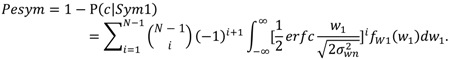
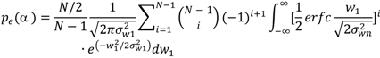
is the average signal-to-noise ratio defined as Jsan 02 00614 i060
This expression was derived by finding the mean values and variance for α as a random variable and analyzing w1 as a random function, as it was done in [15]. The probability of error then can be derived in this closed form
Jsan 02 00614 i041
where the energy of a bit is related to the energy of a chip as Eb = 2βEc.

3.2. N-Correlator Receiver

Following the procedure explained in Section 2.2 for the fading coefficient different from one, i.e., α≠1, the output of the n-th correlator can be expressed as
Jsan 02 00614 i042
having zero mean and variance
Jsan 02 00614 i043
In the case of binary chip symbol transmission the variance is
Jsan 02 00614 i044
From the expressions for a single and N-correlator receiver, we can see that there are two variables that are approximately Gaussian with the mean value zero (for wn) and the mean value that depends on α (for w1). Following the procedure in Section 2.2, the probability of bit error can be expressed as
Jsan 02 00614 i045
In this expression the probability of bit error depends on the fading coefficient α, which is inside the expression for the variance of wn. Therefore the probability of error needs to be calculated as the mean value of this random function to get the probability of bit error for fading channel as
Jsan 02 00614 i046
where variable α has Rayleigh density function defined as
Jsan 02 00614 i047
.

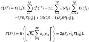
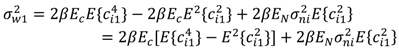
4. Interleaver Communication System Analysis in the Presence of Fading

4.1. Single Correlator Receiver

The fading increases significantly BER inside communications systems. It is assumed that a particular fading coefficient affects each sequence/symbol transmitted. If interleaver/deinterleaver blocks are included into the transceiver structure, as shown in Figure 1, the effects on fading can be spread in a symbol interval. In this paper, it will be assumed that the block interleaver of 2β × 2β size is employed. Thus, the chips for each symbol are written into the interleaver row wise and taken out column wise at the transmitter side. The opposite operation is performed at the receiver side to re-order the chips and return them to be in the corresponding symbol interval. Thus, the samples at the output of receiver multiplexer (MUX) are the chips affected with independent fading coefficients expressed as
Jsan 02 00614 i048
The received chip samples are applied to the chip sequence correlator input. The output sample of the first correlator is
Jsan 02 00614 i049
with its mean
Jsan 02 00614 i050
and variance
Jsan 02 00614 i051
The probability of bit error can be calculated as
Jsan 02 00614 i052
If the source generates binary symbols and the spreading sequence is in binary form, we may have
Jsan 02 00614 i053
This probability depends on a random function which is a sum of 2β Rayleigh distributed random variables. The proabability of error can be calculated as the mean value of Equation (45) in respect to this random function.
This expression was derived by finding the mean values and variance for αi as independent and identically distributed random variables, as it was done in [15]. The probability of error is derived in this closed form
Jsan 02 00614 i054
As can be seen from this expression, the probability of error will decrease as the spreading factor 2β increases.

4.2. N-Correlator Receiver

Following the procedure explained in Section 2.2 for fading coefficient α ≠ 1, the output of the n-th correlator can be expressed as
Jsan 02 00614 i055
which is a realization of a random variable having zero mean and variance
Jsan 02 00614 i056
In the case of binary chips the variance is
Jsan 02 00614 i057
Following the procedure that was presented in Section 3.2, the probability of bit error can be expressed as
Jsan 02 00614 i058
In this expression, the probability of bit error depends on the sum of fading coefficient and their squared values. Therefore, the probability of error needs to be calculated as the mean value of this random function.

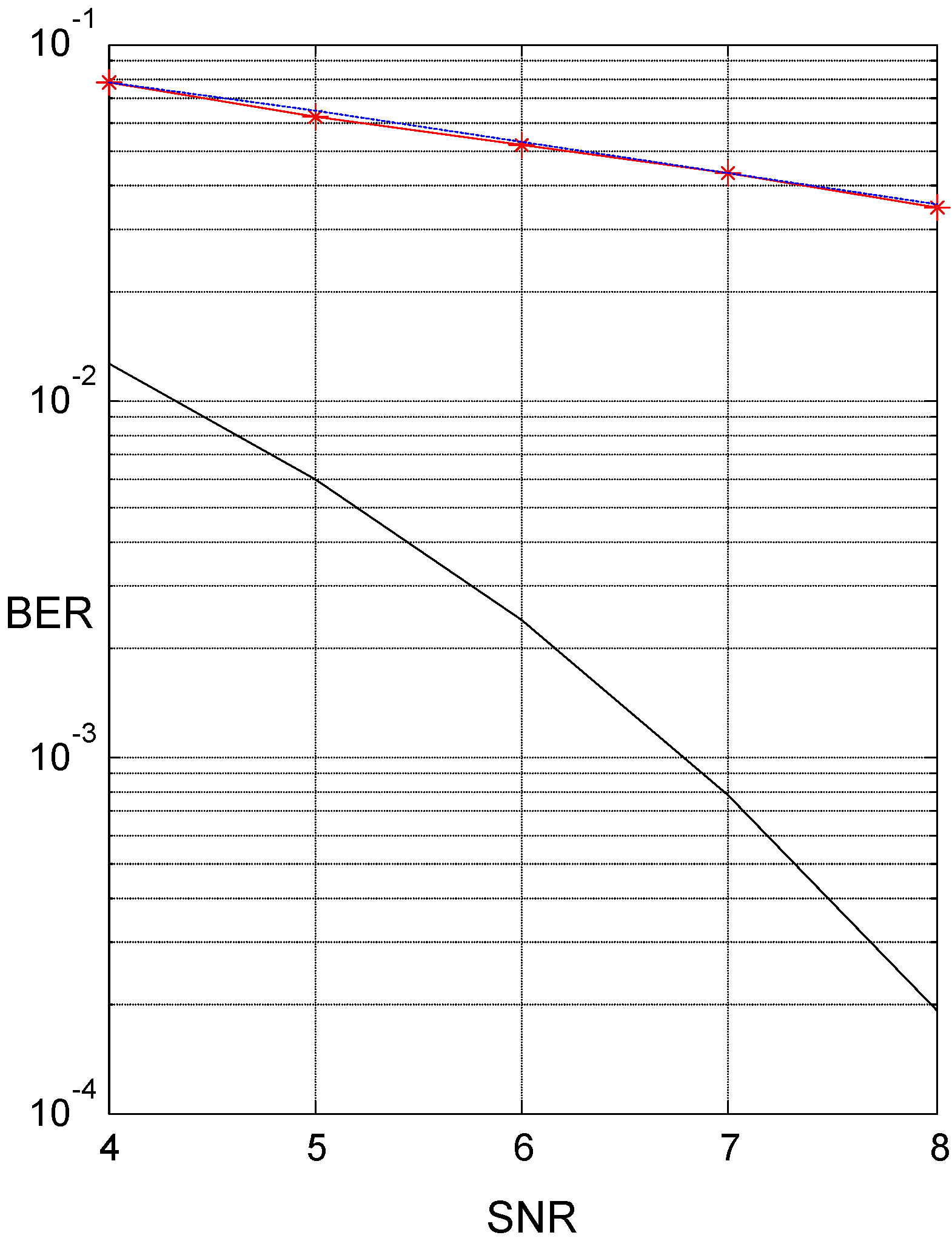
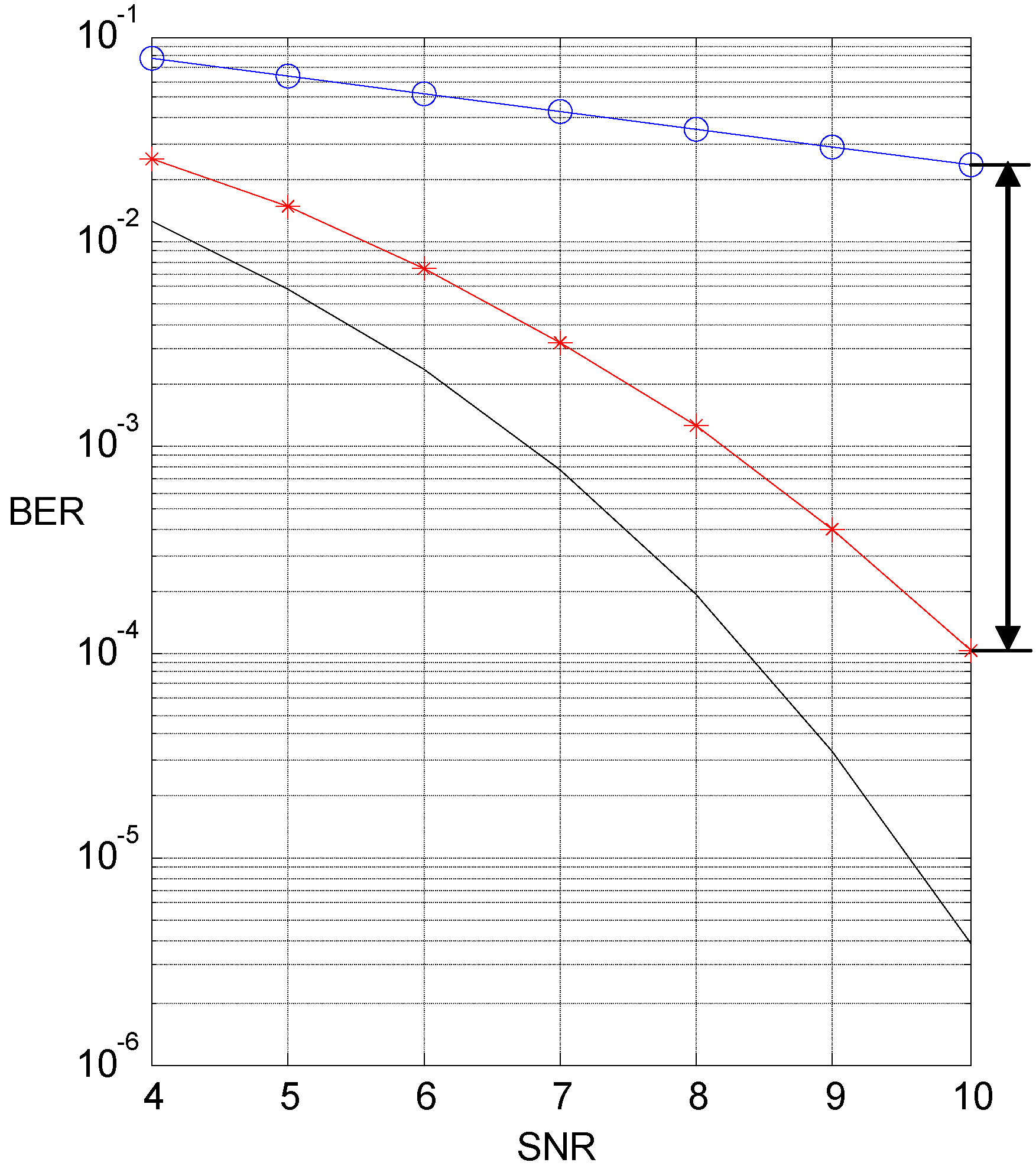
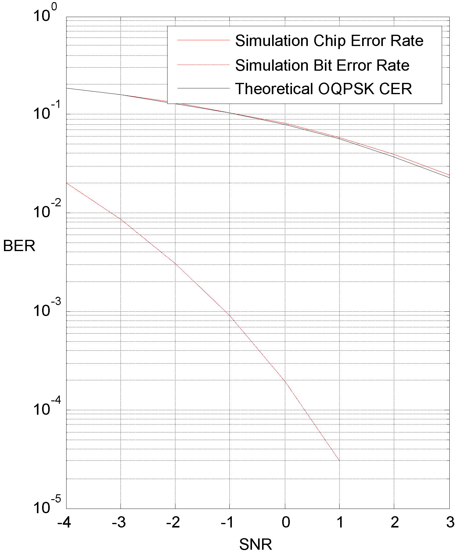
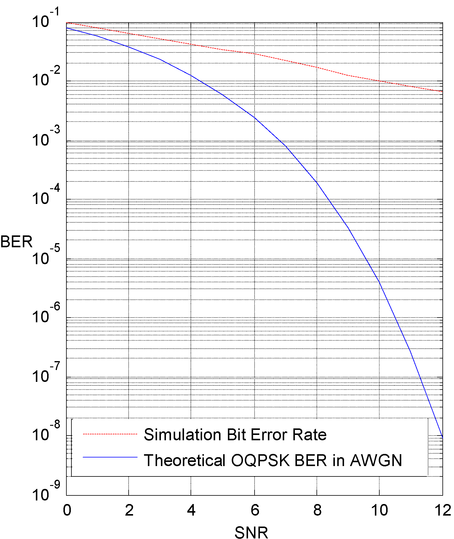
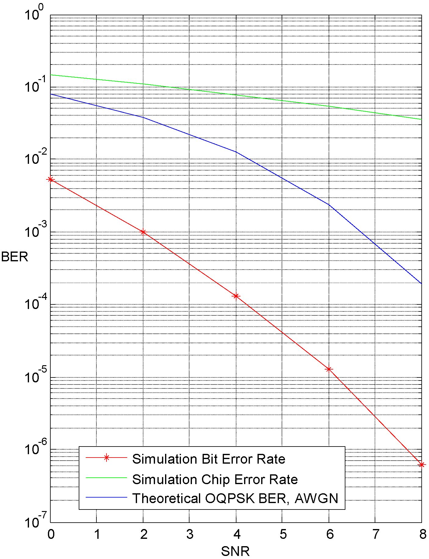
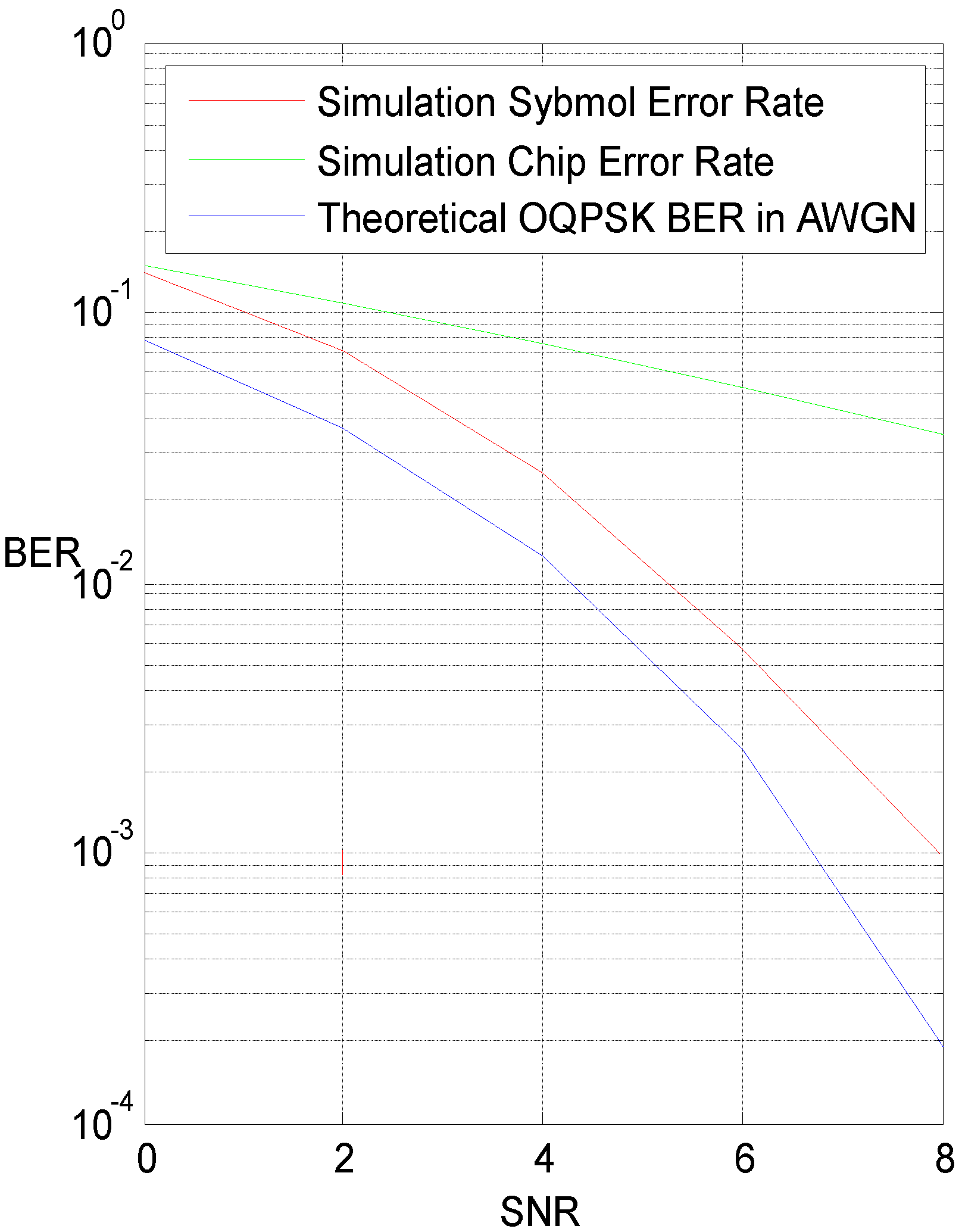
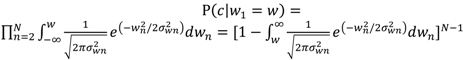
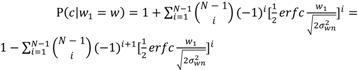
5. Simulation Results and Discussions

The system presented in Figure 1 is simulated in MATLAB. The transmitter, channel and receiver are designed as separate blocks. The channel is designed to generated pass-band noise according to the scheme in Figure 1. The level of the noise is controlled by specifying the value of the noise energy EN. The fading is generated using a fading generator with the empirical density function which corresponds to the theoretical Rayleigh density function.
The simulation was conducted according to the following procedure. The sequence of message bits is generated at the input of the receiver. The spreading sequence is assigned to each bit or the symbol, depending on the systems structure. Then the spreading sequence modulated the carrier using OQPSK modulation, which is defined by the Standard for WSNs [1]. The modulated signal is affected by the noise and fading, which were generated inside the channel. The received signal is demodulated in the block of receiver. At the output of the receiver, the symbols were detected and then transferred into the corresponding bits.
The detected bits are compared with the message bits generated at the input of the system and BER rate is calculated as the ratio of the number of errors detected and the number of bits transmitted. The Chebyshev’s inequality method for accurate estimation of each BER value was used. According to this method it was needed to transmit at least 107 bits to achieve 99% confidence in BER estimates [14]. This BER value estimation was done for each signal to noise ratio that is defined as abscissa value in all Figures presented in this Section.
Two sets of simulators are designed. The first set included simulators with one correlator receiver. In this case the bits were directly related to the spreading sequence as defined by the Standard for WSNs [1]. In this set of simulators, the channel was simulated using either the additive white Gaussian noise channel (AWGN) noise generator or the AWGN generator with fading. In addition, the system was simulated by including or excluding the interleaver and deinterleaver blocks. The second set of simulators included 16 correlators at the receiver side. In this case, the message random bits were transferred into symbols and the spreading sequences are assigned to the symbols according to the Standard specifications [1]. The results of simulation, obtained from both sets of simulators, are presented in this Section.

5.1. Single-Correlator Receiver

In the following simulations, the spreading sequences have been chosen according to the standard for sensor networks [1]. The spreading factor is 2β = 32. The carrier inside in-phase and quadrature branch is modulated by 16 chips representing a symbol. The pulse shaping was done according to the Standard [1]. Figure 2 presents theoretical BER curve (blue) and the curve obtained by simulation (red). The simulated BER is overlapping the theoretical curve from 0 dB to 8dB.
Figure 2. BER curves for a single-correlator receiver in presence of additive white Gaussian noise channel (AWGN): theory (blue) and simulation (red).
Jsan 02 00614 g002
Figure 3 presents theoretical BER curve (blue) and the curve obtained by simulation (red) in the case when fading is present in the channel. The BER is significantly worse than in the case when the AWGN is present in the channel which is represented by the third (black) curve in Figure 3. This is the reason a method of fading mitigation using interleavers and deinterleavers is investigated. The results for this case are shown in Figure 4.
Figure 3. BER curves for a single-correlator receiver in the presence of AWGN and fading: theoretical (blue), simulation (red) for fading, and theory for noise only (black).
Jsan 02 00614 g003
Figure 4. BER curves for a single correlator receiver with interleavers in presence of AWGN and fading: theoretical (blue) for fading, simulated (red) for fading with interleavers and theoretical for noise only (black).
Jsan 02 00614 g004
As can be seen from Figure 4, the improvement in BER is substantial if interleaver and deinterleaver are used. In this simulation a block interleaver is used and BER improvement achieved is, for example, from 2.2 × 10⁻² to 1 × 10⁻⁴ (more than two order of magnitude) for SNR = 10 dB, as can be seen in Figure 4. By using interleavers and deinterleavers the influence of fading inside each symbol is practically randomized and the BER curve is coming closer to the curve representing BER when noise only is present in the channel (black curve). The interleaver curve obtained by the simulation can be easily confirmed by the theoretical Equation (46).
Further improvement could be achieved if the spreading factor is increased. Therefore, the chip interleaving is efficient technique to mitigate fading influence and contributes directly to the power saving in wireless sensor networks. Namely, for the required BER a smaller value of SNR is required if the system includes interleaver and deinterleaver blocks.

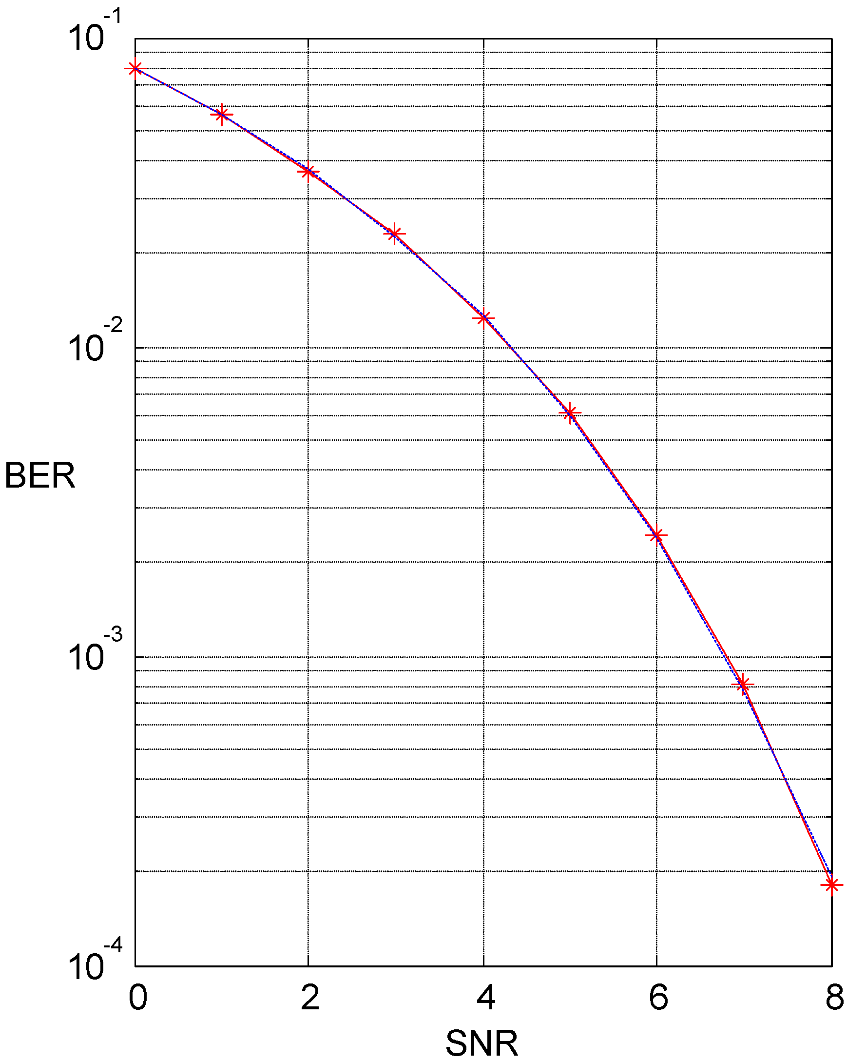
5.2. N-Correlator Receiver

Figure 5 presents BER curves for N=16-correlator receiver with AWGN channel. The black and red overlapping curves are theoretical and simulated chip error rate curves respectively. The dashed red curve is the BER plotted on the same SNR x-axis. There is a processing gain of more than 8dB due to use of the direct sequence spread spectrum technique. The calculated processing gain according to the Standard is about 9 dB with a chip rate of 2.0 MHz and a bit rate of 250 kb/s.
Figure 5. BER curves for 16-correlator receiver in presence of AWGN: theoretical (black) chip error rate (CER), simulation CER (red) and BER on CER SNR scale (red dashed).
Jsan 02 00614 g005
Figure 6 presents BER curves in the case when fading and noise are present in the channel. The blue curve shows theoretical BER for OQPSK and dashed red curve shows BER simulation in the case when noise and fading are present in the channel. It is obvious that the BER values are increasing significantly in the presence of fading. For that reason the interleaver and deinterleaver blocks are introduced into the transceiver structure and the system’s properties are investigated by simulation. The results of simulation are presented in Figure 7.
Figure 6. Rayleigh fading and AWGN are present in the channel.
Jsan 02 00614 g006
Figure 7 presents BER curves in the case when fading and noise are present in the channel and interleaver and deinterleaver blocks are used. The green curve represents the chip error rate in the system. The blue curve shows theoretical BER for OQPSK and red curve shows BER simulation in the case when noise and fading are present in the channel with interleaver and deinterleaver blocks included in the transceiver structure. This curve is plotted on SNR ratio taken on x-axis for chip error rate calculation. It is obvious that the BER values will decrease significantly when the interleaver and deinterleaver are used.
Figure 7. Fading channel and interleaver and deinterleaver are present on the transceiver.
Jsan 02 00614 g007
The expected gain is between 8 and 9 dB. To estimate the gain in BER values the BER curve was shifted for this amount as shown in Figure 8. This Figure gives an estimate where the BER curve will be in respect to the BER curve obtained in AWGN channel. Obviously, the BER curve obtained in the system with interleaver and deinterleaver (red color) tends to the curve obtained when the channel is with AWGN only. Therefore, the system with interleavers is giving significant improvements in BER values.
Figure 8. Estimated position of the BER curve when fading channel and interleavers and deinterleavers are present in communication system.
Jsan 02 00614 g008

6. Conclusions

The paper contains analytical model of a communication system (transmitter, receiver and channel) for physical layer of wireless sensor networks in the case when all signals are represented and processed in discrete time domain suitable for direct design in digital technology. The expressions for BER rate for a single and an N-correlator receiver are derived for discrete time signals for the case when white Gaussian noise and fading are present in the channel. In particular, theoretical model and derivative of the BER are presented for the case when interleavers and deinterleavers are used in the system. The theoretical models complied perfectly with the simulation results. BER expressions for N-correlator receiver are derived in suitable integral form.

Conflict of Interest

The authors declare no conflict of interest.

References

  1. IEEE Standard for Local and Metropolitan Area Networks—Part 15.4: Low-Rate Wireless Personal Area Networks (LR-WPANs); IEEE Standard 802.15.4–2011(Revision of IEEE Std 802.15.4–2006); IEEE: New York, NY, USA, 2011; pp. 1–294.
  2. Wang, C.C.; Huang, C.C.; Huang, J.M.; Chang, C.Y.; Li, C.P. Zig-Bee 868/915-MHz modulator/demodulator for wireless personal area network. IEEE Trans. Very-Large Scale Integr. (VLSI) Syst. 2008, 16, 936–938. [Google Scholar] [CrossRef]
  3. Oh, N.-J.; Lee, S.-G. Building 2.4-GHZ radio transceiver using IEEE 802.15.4. IEEE Circuits Devices Mag. 2006, 21, 43–51. [Google Scholar]
  4. Khalil, I.M.; Gadallah, Y.; Hayajneh, M.; Khreishah, A. An adaptive OFDMA-based MAC protocol for underwater acoustic wireless sensor networks. J. Sens. Actuat. Netw. 2012, 12, 8782–8805. [Google Scholar]
  5. Islam, M.R.; Han, Y.S. Cooperative MIMO communication at wireless sensor network: An error correcting code approach. J. Sens. Actuator Netw. 2011, 11, 9887–9903. [Google Scholar]
  6. Colistra, G.; Atzori, L. Estimation of physical layer performance in WSNs exploiting the method of indirect observations. J. Sens. Actuator Netw. 2012, 1, 272–298. [Google Scholar] [CrossRef]
  7. Gui, X. Chip-interleaving direct sequence spread spectrum system over Rician multipath fading channels. Wirel. Commun. Mob. Comput. 2011. [Google Scholar] [CrossRef]
  8. Mahadevappa, R.H.; Proakis, J.G. Mitigating multiple access interference and intersymbol interference in uncoded CDMA systems with chip-level interleaving. IEEE Trans. Wirel. Commun. 2002, 1, 781–792. [Google Scholar] [CrossRef]
  9. Berber, S.M.; Vali, R. Fading Mitigation in Interleaved Chaos-Based DS-CDMA Systems for Secure Communications. In Proceedings of the 15th World Scientific and Engineering Academy and Society (WSEAS) International Conference on Communications, Corfu, Greece, 15–17 July 2011; pp. 1–6.
  10. Lin, Y.-N.; Lin, D.W. Novel analytical results on performance of bit-interleaved and chip-interleaved DS-CDMA with convolutional coding. IEEE Trans. Veh. Technol. 2005, 54, 996–1012. [Google Scholar] [CrossRef]
  11. Vali, R.; Berber, M.S.; Nguang, K.S. Accurate derivation of chaos-based acquisition phase performance in a fading channel. IEEE Trans. Wirel. Commun. 2012, 11, 722–731. [Google Scholar] [CrossRef]
  12. Vali, R.; Berber, M.S.; Nguang, K.S. Analysis of chaos-based code tracking using chaotic correlation statistics. IEEE Trans. Circuits Syst.-I 2012, 59, 796–805. [Google Scholar] [CrossRef]
  13. Proakis, J.G. Digital Communications, 4th ed.; McGraw-Hill: New York, NY, USA, 2001. [Google Scholar]
  14. Berber, S.M. Bit error rate measurement with predetermined confidence. Inst. Electr. Eng. 1991, 27, 1205–1206. [Google Scholar]
  15. Berber, S.M.; Yuan, Y.; Suh, B. Derivation of BER Expressions and Simulation of a Chip Interleaved System for WSNs Application. In Proceedings of the 17th WSEAS International Conference on Communications, Rhodos, Greece, 16–19 July 2013; pp. 128–133.

