Abstract
In this paper, a compact and low-power true single-phase flip-flop (FF) design with fully static operations is presented. The design is developed by using various circuit-reduction schemes and features a hybrid logic style employing both pass transistor logic (PTL) and static complementary metal-oxide semiconductor (CMOS) logic to reduce circuit complexity. These circuit optimization measures pay off in various aspects, including smaller clock-to-Q (CQ) delay, lower average power, lower leakage power, and smaller layout area; and the transistor-count is only 17. Fabricated in TSMC 180 nm CMOS technology, it reduces by over 29% the chip area compared to the conventional transmission gate FF (TGFF). To further show digital circuit/system level advantages, a multi-mode shift register has been realized. Experimental measurement results at 1.8 V/4 MHz show that, compared with the TGFF design, the proposed design saves 64.7% of power consumption while reducing chip area by 26.2%.
1. Introduction
With the growth of the Internet of Things (IoT) and wearable devices, the need for ultra-low power consumption SOC chips is increasing [1]. The speed performance is no longer the focus of research works; instead, the power consumption and layout area are key points in the design [2]. Flip-flop (FF) is the basic storage block used widely in digital very large-scale integer (VLSI) designs, which adopt intensive pipelining schemes and employ many FF-rich modules such as shift register, FIFO (first in first out) and register file. In a commercial SPARCT4 processor, there are more than 2 million FFs consuming over 20% of the total power consumption of the processor [3]. Also, in an ARM Cortex-M0 processor with minimum instruction and data memories, they are synthesized from standard cells for IoT applications. In this design, FFs account for 40% of the chip area and 30% of the total power consumption [4]. Therefore, FF design is critical to the power consumption performance of the system design and also has a significant impact on chip area. FF design continues to evolve with the development of new process technologies. Specific application requirements such as low voltage, low power consumption, or high performance also require new designs [4,5,6,7,8,9,10,11,12,13,14,15,16,17]. In this work, the target is a low-power and low-circuit complexity FF design solution. A transmission gate-based FF (TGFF) is the most widely used one today. One of the drawbacks of this FF design is the excessive loading on the clock signal (a total of 12 transistors driven by the clock signal) as shown in Figure 1a. As a result, there is considerable dynamic power consumption even when the input data signal switching activity is zero or low. This problem also occurs in conventional SR-latch-based FF (SRFF) designs, as shown in Figure 1b.
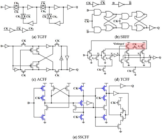
Figure 1.
Representative flip-flop (FF) designs. (a) Transmission gate-based FF (TGFF). (b) SRFF. (c) adaptive coupling FF (ACFF). (d) topologically compressed FF (TCFF). (e) static contention free single-phase-clocked FF (SSCFF).
Recently, true single-phase clocking (TSPC)-based FF designs are discussed for low power applications. The basic idea is mitigating the load capacitance of clock signal by using logic and circuit simplification [9,10,11,12]. In this paper, a novel SR latch-based FF using hybrid logic circuit scheme is presented. It follows the principle of TSPC operations to reduce the clock signal loading. The design exhibits a lowest transistor-count and a shorter critical path when compared with previous FF designs.
2. Proposed Flip-Flop (FF) Design
2.1. Previous Low-Power FF Designs
To mitigate the power consumption problem of TGFF design, three low-power FFs have been proposed. Figure 1c shows the adaptive coupling (AC) flip-flop design [9]. Unlike traditional TGFF designs, this design uses a differential latch structure with pass transistor logic (PTL) to achieve true single-phase clock operation. To overcome the effects of process variation on the master latch, a pair of level recovery circuits were inserted into the cross-coupled path. In this FF design, the clock drives only 4 transistors, and the total number of transistors is 22. When the FF is operating at low and/or zero data-switching activity, lighter clock loads and reduced circuitry in the FF design can significantly reduce dynamic power consumption. However, the pMOS type pass transistor-based latch design results in a longer setup time even in the presence of a level recovery circuit. Finally, there are floating problems in some nodes inside this FF design, which impose limitations on the applications of ACFF design [10].
Figure 1d shows another low-power FF design using a topologically compressed scheme, named TCFF based on SR-latch circuit structure [11]. Even though the pull-up and pull-down logic networks are greatly simplified, and the respective logic topologies are no longer dual to each other, the design is fully static. Despite the improved power performance, the design’s timing parameters deteriorate. Similar to the ACFF design, this design also requires a large setup time because the pull-up network is weakened. The critical path consists of 3 pMOS transistors in series. Although this circuit problem can be mitigated by increasing the metal-oxide semiconductor (MOS) transistor size, both low-power and low transistor-count advantages of the FF design will be compromised [10]. Figure 1e shows the static contention free single-phase-clocked flip-flop, named SSCFF, aimed at alleviating these problems [12]. It is composed of a conventional dynamic TSPC-based FF design with 9 transistors colored in blue and an additional 15 transistors to ensure its fully static circuit operations and sufficient output drive capability. This FF design provides better power and energy performance compared to traditional TGFF design. However, the height of its pull-down logic added up to three. This calls for large size transistors and results in a larger layout area [10].
2.2. Proposed FF Design
In view of these shortcomings of previous low-power FF designs, an enhanced design that applies further circuit structure simplification schemes to ACFF designs is proposed. Referring to Figure 2, the proposed design adopts hybrid logic style circuit i.e., a static CMOS style SR-latch at master stage and a pass transistor logic style SRAM-based latch at slave stage, to reduce circuit complexity. The proposed circuit design contains 19 transistors as shown in Figure 2. Based on this MOS transistor schematic, at the transistor level the following steps are used to further reduce the number of n-MOS transistors. For pull-down logic, one signal “R” controlled the nMOS transistor can be shared by two discharging paths as shown in Figure 3a. Note that when the clock signal CK is high, the transistor N1 of the master latch keeps the input stage. In this case, transistor N2 (inverter I2) of the slave-latch is also turned on. Thus, the slave latch also provides a discharging path for the master latch as shown in Figure 3b. As a result, it can eliminate the clock-driven redundancy of one n-MOS transistor and simplify the circuit. This measure cannot only reduce power consumption and layout area, but also reduce the capacitive load of the clock. In general, when using fewer transistors to realize a fully static design, the leakage power consumption reduces as well. The simplified schematic of the final circuit after applying logic and circuit reduction is shown in Figure 3c. The total transistor count in our design is 17 (8 pMOS transistors and 9 nMOS transistors). This FF design uses one (true) phase of the clock signal and only 5 transistors are driven by the clock signal.
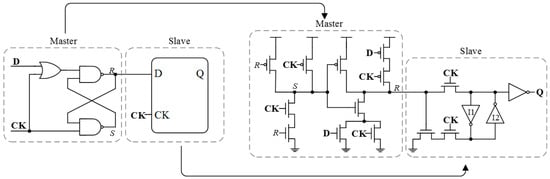
Figure 2.
Schematic of proposed design.
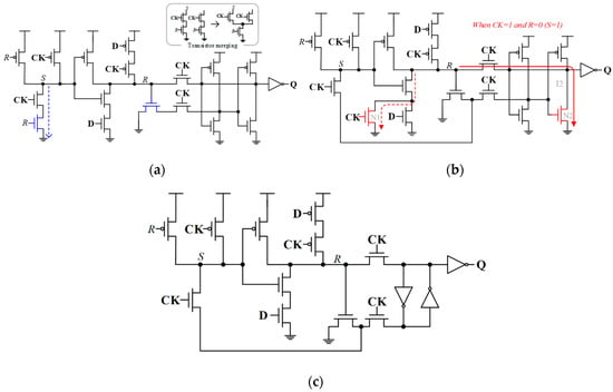
Figure 3.
Proposed FF design. (a) Transistor merging in pull-down nMOS. (b) Transistor removing in pull-down nMOS. (c) Proposed FF design with 17 transistors.
The proposed design uses a hybrid of fully complementary logic (AOI gate) and pass transistor logic in the FF circuit design. It successfully achieves the purpose of simultaneously increasing the timing parameter and reducing the circuit complexity. Figure 4; Figure 5 show the operation of the proposed design at different input signals (clock and data) cases operations, and the post layout simulation waveforms of our design, respectively. The FF design operates correctly in all cases, and all nodes have a complete voltage swing.
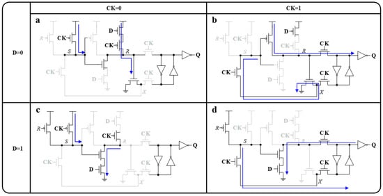
Figure 4.
Proposed FF operation diagram at different inputs cases (highlighting the active devices).
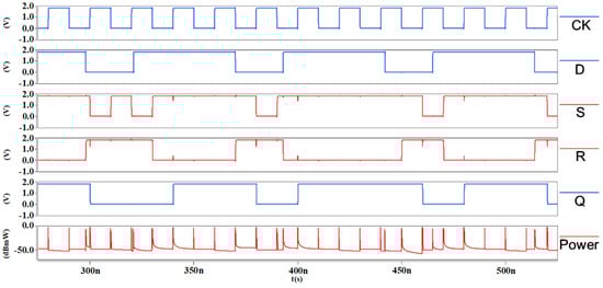
Figure 5.
Waveforms on HSPICE of proposed design.
3. Simulation Results
In order to fully evaluate the performance of the proposed FF design, post-layout simulations of various FF designs were conducted. Two classic master-slave based FF designs TGFF, SRFF and three low-power designs, i.e., ACFF [9], TCFF [11] and SSCFF [12] as shown in Figure 1, were included in comparisons. Besides the TCFF design, which basically trades its timing performance for power saving, an alternative design (denoted as *TCFF) using enlarged pMOS transistors to enhance its pull up driving capability was also evaluated. However, pulse-triggered based FF designs are excluded deliberately because they usually require a complicated transistor size tweaking process to ensure correct trigger timing and pulse width for different settings of VDD and working frequency. The design resilience to the process variations is another concern associated with these designs [14,15,16,17]. Note that, a TSPC-based FF design using 18-transistors is proposed in [18]. However, there are floating problems in some nodes inside this low-complexity and low-power FF design. Moreover, to ensure lower VDD operation, a back-bias voltage scheme was employed to reduce the threshold voltage, so it is not included in the discussion. The decision to use 180 nm technology is for emerging low-power applications where power performance rather than running speed is the ultimate concern. Therefore, it is cost effective to use more mature technology than to switch to advanced technology. In addition, compared with more advanced processes, the leakage power and process variation of the 180 nm process are relatively low.
The size of the transistor depends on the optimization of power-delay-product (PDPCQ) and the function at normal VDD (1.8v). Note that, in *TCFF, the width of the pMOS transistors is increased to provide better setup time performance. All input signals are also generated through buffers to account for the effects of rise/fall time delays. The operating condition used in simulations is 50 MHz/1.8 V. Five test patterns, each showing a different data-switching activity, were used in simulations. The switching activity ranged from 0% to 100% (input data signal toggles on every clock signal cycle). The model setup for FF simulations in this work is shown in Figure 6. To mimic a realistic scene, it had one clock buffer driving 8 FFs. The current driving into FFs was measured and then divided by 8. Thus, measured average power consumption in this work also considered the clock-driving power consumption. The post-layout simulation results including circuit complexity, timing parameter, average power consumption, energy consumption (power-delay-product), and leakage power consumption are summarized in Table 1.
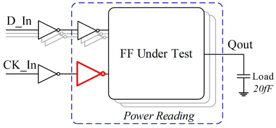
Figure 6.
Test bench for FF design simulations.

Table 1.
Comparison summary of various FFs @50 MHz/1.8 V/TT-Corner.
In terms of circuit complexity, the proposed design uses the fewest number of transistors and has the smallest layout area in all FF designs. As for the power consumption behavior as shown in Figure 7a, our design is the most power efficient in all but one case (when the input is static, i.e., 0% switching probability, the proposed design is slightly inferior to both ACFF and TCFF design). Compared with traditional TGFF design, the proposed design achieves power consumption saving from 31.3% to 51.1%. Compared with TCFF (*TCFF), ACFF and SSCFF designs, the power advantage of the proposed design is maximized when the data-switching probability is 100%. The average power consumption saving is up to 52.6% against the ACFF design. For the case of 12.5% data-switching activities, the average power consumption saving against TGFF, SRFF, ACFF, TCFF(*TCFF) and SSCFF were 51.1%, 55.7%, 23.0%, 2.0%(24.2%), and 34.3%, respectively. Figure 7b shows the comparison of average power consumption at different operating frequencies. The input signal switching activity was set to 12.5%. The proposed design is the best power efficiency in all cases. Although the ACFF design has a competitive advantage in the lower switching activity, as the switching activity increases, its power performance will rapidly decrease. The main reason is the frequent level of switching and contention issues in its master and slave latches. The SRFF and TGFF design have the worst power consumption performance because they have a higher clock tree loading than other true-signal-phase clocking-based FF designs. The average power consumption @12.5% switching under different VDD settings (from 1.8V to 1.0 V) is shown in Figure 7c. The working frequency was lowered to 10 MHz to ensure that all FF designs functioned properly in low VDD settings. The SRFF design exhibited the highest power in all cases. The TGFF design was ranked second, followed by the SSCFF and ACFF. The proposed design and the TCFF design exhibited the lower power consumption.
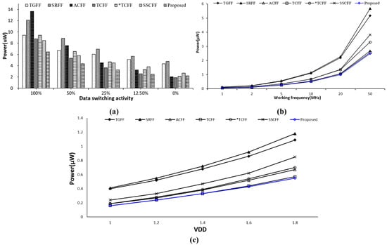
Figure 7.
Simulation results for power consumption comparison for (a) different switching activity factors; (b) different operation frequencies; (c) different operation supply voltages.
Besides the power consumption, the PDP index (the product of the CQ delay and the power consumption) was employed as a composite performance index in this work. When the data switching activity was 12.5%, the PDP of the proposed design was 17.0%~79.5% lower than those of the compared FF designs. A bar chart summarizing the PDP comparison results under different data switching activities is given in Figure 8a. Figure 8b shows the PDP performance against process variations with a 12.5% data-switching activity. For each process corner, the setup time value is scanned for the best PDP number. Even all FF designs can operate normally with process variations. The proposed design has the best PDP performance in all cases. This proves the consistent performance edge of the proposed design. Notably, both TGFF and SRFF designs have the worst PDP performances.
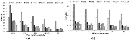
Figure 8.
Simulation results for power-delay-product (PDP) performances. (a) Different switching activity factors. (b) Different process corners.
Regarding the timing parameters of the FF designs, Table 1 also lists the setup time, the hold time, and the CQ delay of these designs (@50 MHz/1.8 V). As explained before, the setup times of ACFF and TCFF (even the version with enlarged pMOS *TCFF) are both much larger than that of the TGFF. This is because these two designs adopt weak pull-up logic structures for power consumption reduction at the cost of inferior timing. In fact, if TCFF uses a typical size i.e., pMOS = 1.20 u, its setup time will be 7 times that of the conventional TGFF design. By using hybrid logic style scheme and removing the redundant discharging path at both master and slave latch, our design improves the setup time and clock to Q delay significantly when compared with the ACFF and TCFF (*TCFF) designs. Regarding the hold-time, all FFs had negative hold times, except for our design. The hold time of the proposed design must be positive value to ensure the completion of input data transition in the slave latch. The proposed design also leads in the clock to Q delay. The delay is 9.5% shorter than the nearest rival, i.e., the SSCFF design. Figure 9 displays the variations in both setup and hold time subject to process variations. Due to the circuit simplification of the pull-up network, the setup time fluctuations of the low-power TCFF and ACFF designs are significantly larger than the traditional TGFF designs. Although the proposed design also uses logic and circuit structure minimization techniques, the setup time and the hold time variation was well confined due to its circuit simplicity.

Figure 9.
Simulation results for timing variation under different process corners. (a) Setup time. (b) Hold time.
In term of leakage power consumption, our design shows the lowest leakage power due to its circuit complexity (17-transistor only). The leakage power saving against the conventional TGFF design is 25.5%. As mentioned before, due to the floating problem of some internal nodes in ACFF design, its leakage power consumption will be the largest among all comparison circuits [10]. Post-layout simulation results also show that the power consumption of the ACFF design is over 2.4 times that of the conventional TGFF design in this particular case, which should not be overlooked when the ACFF design is employed in the low power applications. Figure 10 presents the Monte Carlo simulation results of PDPCQ derived by executing 1000 runs. Three FF designs, i.e., TGFF, ACFF, and the proposed design are simulated. The plot has a format of power consumption as the x-axis and the CQ delay as the y-axis. Therefore, the closer the point is to the lower left part of the plot, the better the performance of this design. From the simulation results, the advantage of our design is obvious in simulation trials.

Figure 10.
Monte Carlo simulation results.
Finally, Figure 11 shows the layout schematic of these FF designs. The height of all FF designs is fixed at 5.15 μm and layers up to metal-2 (M2) are used in drawing the layout schematic. The layout-area size of our design is only 5.15 μm by 8.0 μm. The area saving against the TGFF design is 29.3%. It should be noted that, although ACFF and TCFF have fewer transistors than the traditional TGFF design, in order to ensure that the operation requirements of all process variations are met, a larger transistor size is required to increase the layout area. It is no surprise that the *TCFF design has the worst layout area to increase the size of pMOS transistors (as shown in Figure 10) in order to improve the setup-time performance. Finally, the layout area of SSCFF is 10% larger than the TGFF design due to its need for a larger transistor and complexity layout structure.
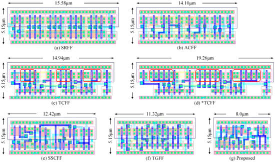
Figure 11.
Layout of FFs.
4. Chip Implementation and Measurement Results
The proposed design and TGFF design further extended to a multi-mode 32-bit shift register (providing 4 × 8bit and 1 × 32bit modes) [18]. This implemented chip is further combined with a ATMEL® 8-bit microcontroller ATmega-328P (which is used in the Arduino UNO board) to further verify its function as shown in Figure 12. The chip design in this work is mainly used with a smart-agricultural embedded system design based on the Arduino platform to monitor the environmental information of a greenhouse. The implemented chip acts as a buffer between the microprocessor (328P) and the SPI (serial peripheral interface bus) interface to reduce the time required for the microprocessor to read these sensors to achieve power consumption as shown in Figure 12c. Note that the standard operating voltage of the ATmega-328P is 3.3 V. In order to combine our chip, we set the relevant fuse to reduce the operating voltage of the ATmega-328P to the lowest 1.8 V by programming [19]. At the same time, the operating frequency uses its built-in oscillator and sets the operation frequency at 8 MHz. The test platform used is shown in Figure 13a and combines an oscilloscope (GWINSTEK GDS-1054B) and a power supply (GWINSTEK GDP-3303S). Figure 13b shows chip measurement waveforms of the proposed design. Each signal from up to down is the clock signal, the input D0, and the output Q31. The operation frequency is 4MHz and the measurement results is shown in Table 2 (the measured power consumption results recorded in Table 2 are the average of 8 chips). Compared with the traditional TGFF-based design, due to its circuit novelty, our design reduces by more than 64.7% the power consumption, while the layout area is reduced by 26.2%. All the above results demonstrate that the proposed design has lower power consumption and lower layout-area than other FF designs. Hence the proposed design is suitable for low-power applications.
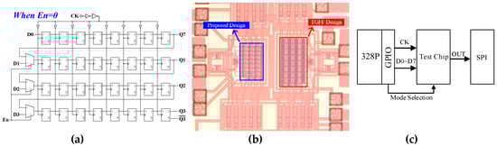
Figure 12.
A multi-mode 32-bit shift register. (a) On-chip configuration for the testing. (b) Die photographic. (c) Platform implemented in this work.
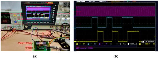
Figure 13.
Photographic of, (a) test setup and, (b)measurement waveforms (1 × 32bit mode).
Table 2.
Simulation and experimental results for the design.
5. Conclusions
In this paper, a novel low-complexity and low-power flip-flop design with fully static operations is proposed. This design uses an SR latch structure and combines a mixed logic circuit style solution for low-power applications. A comprehensive evaluation shows that of all the compared FF designs, the proposed design is the most economical in terms of power and energy consumption. It also requires the smallest chip area. Our designs can thus be used in cell library designs for power- and energy-critical applications.
Author Contributions
J.-F.L. and Z.-J.H. proposed the idea and method; C.-M.T. and S.-W.Y. performed the simulations and experiments; B.-C.W. and Z.-J.H. analyzed the data; J.-F.L. reviewed the manuscript. All authors have read and agreed to the published version of the manuscript.
Funding
This work was supported by the Ministry of Science and Technology, Taiwan under contract No. 107-2221-E- 324-017-MY2 and a grant (Grant No. 109AS-11.3.2-ST-a9) from the Council of Agriculture, ROC.
Acknowledgments
The authors also thank the National Chip Implementation Center (CIC), Taiwan for technical support in simulations.
Conflicts of Interest
The authors declare no conflict of interest.
References
- Atzori, L.; Iera, A.; Morabito, G. The Internet of Things: A survey. Comput. Netw. 2010, 54, 2787–2805. [Google Scholar] [CrossRef]
- Chang, K.-L.; Gwee, B.-H.; Chang, J.S.; Chong, K.-S. Synchronous logic and asynchronous-logic 8051 microcontroller cores for realizing the Internet of Things: A comparative study on dynamic voltage scaling and variation effects. IEEE J. Emerg. Sel. Top. Circuits Syst. 2013, 3, 23–34. [Google Scholar] [CrossRef]
- Shin, J.L.; Golla, R.; Li, H.; Dash, S.; Choi, Y.; Smith, A.; Sathianathan, H.; Joshi, M.; Park, H.; Elgebaly, M.; et al. The next generation 64b SPARC core in a T4 SoC processor. IEEE J. Solid-State Circuits 2013, 48, 82–90. [Google Scholar] [CrossRef]
- Moreau, L.; Rémi, D.; David, B. A 0.4 V 0.5 fJ/cycle TSPC flip-flop in 65nm LP CMOS with retention mode controlled by clock-gating cells. In Proceedings of the 2019 IEEE International Symposium on Circuits and Systems, Sapporo, Japan, 26–29 May 2019. [Google Scholar]
- Partovi, H.; Burd, R.; Salim, U.; Weber, F.; DiGregorio, L.; Draper, D. Flow-through latch and edge-triggered flip-flop hybrid elements. In Proceedings of the 1996 IEEE International Solid-State Circuits Conference. Digest of TEchnical Papers, ISSCC, San Francisco, CA, USA, 10 February 1996; pp. 138–139. [Google Scholar]
- Stojanovic, V.; Oklobdzija, V. Comparative analysis of master-slave latches and flip-flops for high-performance and low-power systems. IEEE J. Solid State Circuits 1999, 34, 536–548. [Google Scholar] [CrossRef]
- Klass, F.; Amir, C.; Das, A.; Aingaran, K.; Truong, C.; Wang, R.; Mehta, A.; Heald, R.; Yee, G. A new family of semi-dynamic and dynamic flip flops with embedded logic for high- performance processors. IEEE J. Solid State Circuits 1999, 34, 712–716. [Google Scholar] [CrossRef]
- Tschanz, J.; Narendra, S.; Chen, Z.; Borkar, S.; Sachdev, M.; De, V. Comparative delay and energy of single edge-triggered and dual edge triggered pulsed flip-flops for high-performance microprocessors. In Proceedings of the 2001 International Symposium on Low Power Electronics and Design, Hillsboro, OR, USA, 6–7 August 2001; pp. 207–212. [Google Scholar]
- Teh, C.K.; Fujita, T.; Hara, H.; Hamada, M. A 77% energy saving 22-transistor single phase clocking D-flip-flop with adoptive-coupling configuration in 40 nm CMOS’. In Proceedings of the 2011 IEEE International Solid-State Circuits Conference, San Francisco, CA, USA, 20–24 February 2011; pp. 338–339. [Google Scholar]
- Lin, J.F.; Sheu, M.H.; Hwang, Y.T.; Wong, C.S.; Tsai, M.Y. Low-power 19-transistor true single-phase clocking flip-flop design based on logic structure reduction schemes. IEEE Trans. Very Large Scale Integr. (VLSI) Syst. 2017, 25, 3033–3044. [Google Scholar] [CrossRef]
- Kawai, N.; Takayama, S.; Masumi, J.; Kikuchi, N.; Itoh, Y.; Ogawa, K.; Ugawa, A.; Suzuki, H.; Tanaka, Y. A fully static topologically-compressed 21-transistor flip-flop with 75% power saving. IEEE J. Solid State Circuits 2014, 49, 2526–2533. [Google Scholar] [CrossRef]
- Kim, Y.; Jung, W.; Lee, I.; Dong, Q.; Henry, M.; Sylvester, D.; Blaauw, D. A static contention-free single-phase-clocked 24T flip-flop in 45 nm for low-power applications. In Proceedings of the 2014 IEEE International Solid-State Circuits Conference Digest of Technical Papers (ISSCC), San Francisco, CA, USA, 9–13 February 2014; pp. 466–467. [Google Scholar]
- Consoli, E.; Alioto, M.; Palumbo, G.; Rabaey, J. Conditional push-pull pulsed latch with 726 fJ•ps energy delay product in 65nm CMOS. In Proceedings of the 2012 IEEE International Solid-State Circuits Conference Digest of Technical Papers (ISSCC), San Francisco, CA, USA, 19–23 February 2012; pp. 482–483. [Google Scholar]
- Alioto, M.; Consoli, E.; Palumbo, G. Analysis and comparison in the energy-delay-area domain of nanometer CMOS flip-flops: Part I-Methodology and design strategies. IEEE Trans. Very Large Scale Integr. (VLSI) Syst. 2011, 19, 725–736. [Google Scholar] [CrossRef]
- Alioto, M.; Consoli, E.; Palumbo, G. Analysis and comparison in the energy-delay-area domain of nanometer CMOS flip-flops: Part II–Results and figures of merit. IEEE Trans. Very Large Scale Integr. (VLSI) Syst. 2011, 19, 737–750. [Google Scholar] [CrossRef]
- Zhao, P.; McNeely, J.; Kuang, W.; Wang, Z. Design of sequential elements for low power clocking system. IEEE Trans. Vlsi Syst. 2011, 19, 914–918. [Google Scholar] [CrossRef]
- Jeong, H.; Oh, T.W.; Song, S.C.; Jung, S.-O. Sense-amplifier-based flip-flop with transition completion detection for low-voltage operation. IEEE Trans. Very Large Scale Integr. (VLSI) Syst. 2018, 26, 609–620. [Google Scholar] [CrossRef]
- Stas, F.; Bol, D. A 0.4-V 0.66-fJ/cycle retentive true-single-phase clock 18T flip-flop in 28-nm fully-depleted SOI CMOS. IEEE Trans. Circuits Syst. I Reg. Pap. 2018, 65, 935–945. [Google Scholar] [CrossRef]
- Yang, B.-D. Low-Power and Area-Efficient Shift Register Using Pulsed Latches. IEEE Trans. Circuits Syst. I Regul. Pap. 2015, 62, 1564–1571. [Google Scholar] [CrossRef]
© 2020 by the authors. Licensee MDPI, Basel, Switzerland. This article is an open access article distributed under the terms and conditions of the Creative Commons Attribution (CC BY) license (http://creativecommons.org/licenses/by/4.0/).