Article

Design of Soft-Switching Hybrid DC-DC Converter with 2-Phase Switched Capacitor and 0.8nH Inductor for Standard CMOS Process

1
Department of Electrical and Computer Engineering, Seoul National University, Seoul 08826, Korea
2
System LSI Business, Samsung Electronics, Hwaseong 18848, Korea
*
Author to whom correspondence should be addressed.
Electronics 2020, 9(2), 372; https://doi.org/10.3390/electronics9020372
Submission received: 30 January 2020 / Revised: 19 February 2020 / Accepted: 19 February 2020 / Published: 21 February 2020
(This article belongs to the Section Circuit and Signal Processing)

Abstract

:
A soft-switching hybrid DC-DC converter with a 2-phase switched capacitor is proposed for the implementation of a fully-integrated voltage regulator in a 65 nm standard CMOS process. The soft-switching operation is implemented to minimize power loss due to the parasitic capacitance of the flying capacitor. The 2-phase switched capacitor topology keeps the same resonance value for every soft-switching operation, resulting in minimizing the voltage imbalance of the flying capacitor. The proposed adaptive timing generator digitally calibrates the turn-on delay of switches to achieve a complete soft-switching operation. The simulation results show that the proposed soft-switching hybrid DC-DC converter with a 2-phase 2:1 switched capacitor improves the efficiency by 5.1% and achieves 79.5% peak efficiency at a maximum load current of 250 mA.

1. Introduction

Recently, developing a fully integrated voltage regulator (FIVR) is one of the design challenges for digital systems [1,2,3,4]. Instead of the conventional external voltage regulation, FIVR can supply the power to the digital system directly without PCB and package interconnections. FIVR can improve system efficiency with fine-grained dynamic voltage frequency scaling (DVFS). Furthermore, since FIVR eliminates the parasitic inductance and resistance of package, as well as PCB between the external voltage regulator and internal digital system, it reduces supply-voltage fluctuation and consequently minimizes the supply-voltage margin of logic cells.
Over the years, switched-capacitor (SC) DC-DC converters have been researched for FIVRs with on-chip or in-package high-density capacitors [5,6,7]. Capacitor-integration technology continues to develop rapidly, while inductor integration is not improving much. Although the SC DC-DC converter can be implemented with the integrated high-density capacitors, there is a limitation to implementing the wide-range input and output with high efficiency. The SC DC-DC converter can achieve high efficiency at only certain conversion ratios determined by the topology due to the charge sharing loss between capacitors. For example, a 2:1 SC DC-DC converter shows high efficiency at only the output voltage of half of the input voltage. To overcome it, reconfigurable SC topologies which support many conversion ratios were presented [8,9]. The reconfigurable SC can provide the wide-range input and output by adjusting conversion ratios based on the input voltage and required output voltage. However, it requires many switches and cascaded connections from input to output, and so the maximum output current is limited by large conduction losses. To overcome these drawbacks, hybrid converters have been introduced [10,11,12]. A small inductor is inserted between the flying capacitor and the output capacitor to eliminate the charge sharing loss. Furthermore, the hybrid converter can support wide-range input and output voltages by controlling the duty cycle, like the conventional inductor-based switching DC-DC converter.
However, in a standard CMOS process, the parasitic capacitor of metal-oxide-metal (MOM), metal-insulator-metal (MIM), and MOS capacitors still degrade the overall efficiency, since additional power is required to charge and discharge the parasitic capacitor [13,14]. Compared to the external capacitors such as a multi-layer ceramic capacitor, the capacitors implemented in a standard CMOS process have a low capacitance density and a high parasitic capacitance, which can greatly degrade overall efficiency. Therefore, in order to improve power efficiency, low-parasitic capacitors such as MOS capacitors in silicon on insulator (SOI) or deep-trench silicon capacitors are required, which significantly increases the overall cost [6].
In this paper, a fully-integrated hybrid DC-DC converter with an adaptive dead-time technique and a 2-phase SC is proposed to eliminate the effects due to the parasitic capacitance of the capacitors in a standard CMOS process.

2. Proposed Soft-Switching Hybrid DC-DC Converter

An example of 2:1 SC topology with the parasitic capacitor of the flying capacitor, Cpar, is shown in Figure 1. To charge Cpar, additional current Ipar flows from the input, and to discharge Cpar, Ipar flows to ground. As a result, it consumes additional power. The power loss, Ploss, caused by Cpar, is determined as follow:
P l o s s = C p a r V I N 2 2 f S W
where vIN is the input voltage and fsw is the switching frequency of the converter. Among the capacitors in a standard CMOS process, the MOS capacitor generally shows a high capacitance density of 4 nF/mm2 up to 12 nF/mm2 while it has a bottom-plate parasitic capacitance of around 10%. Although MIM and MOM capacitors have lower parasitic capacitances of around 1.5%, these show lower capacitance densities of up to 2 nF/mm2 [6,15]. For example, if a 2 nF flying capacitor with a 5% parasitic capacitance is implemented for the FIVR, the power loss due to Cpar can be tens of milliwatts. To overcome it, the SC DC-DC converter shown in [15] proposed the scalable parasitic charge redistribution technique with multi-phase SCs. By redistributing the charge of the parasitic capacitor to another flying capacitor of the opposite-phase SC instead of discharging to ground, it can improve the power efficiency of the converter implemented in a standard CMOS process. However, it is still an SC architecture, so it can not support wide-range input and output voltages.
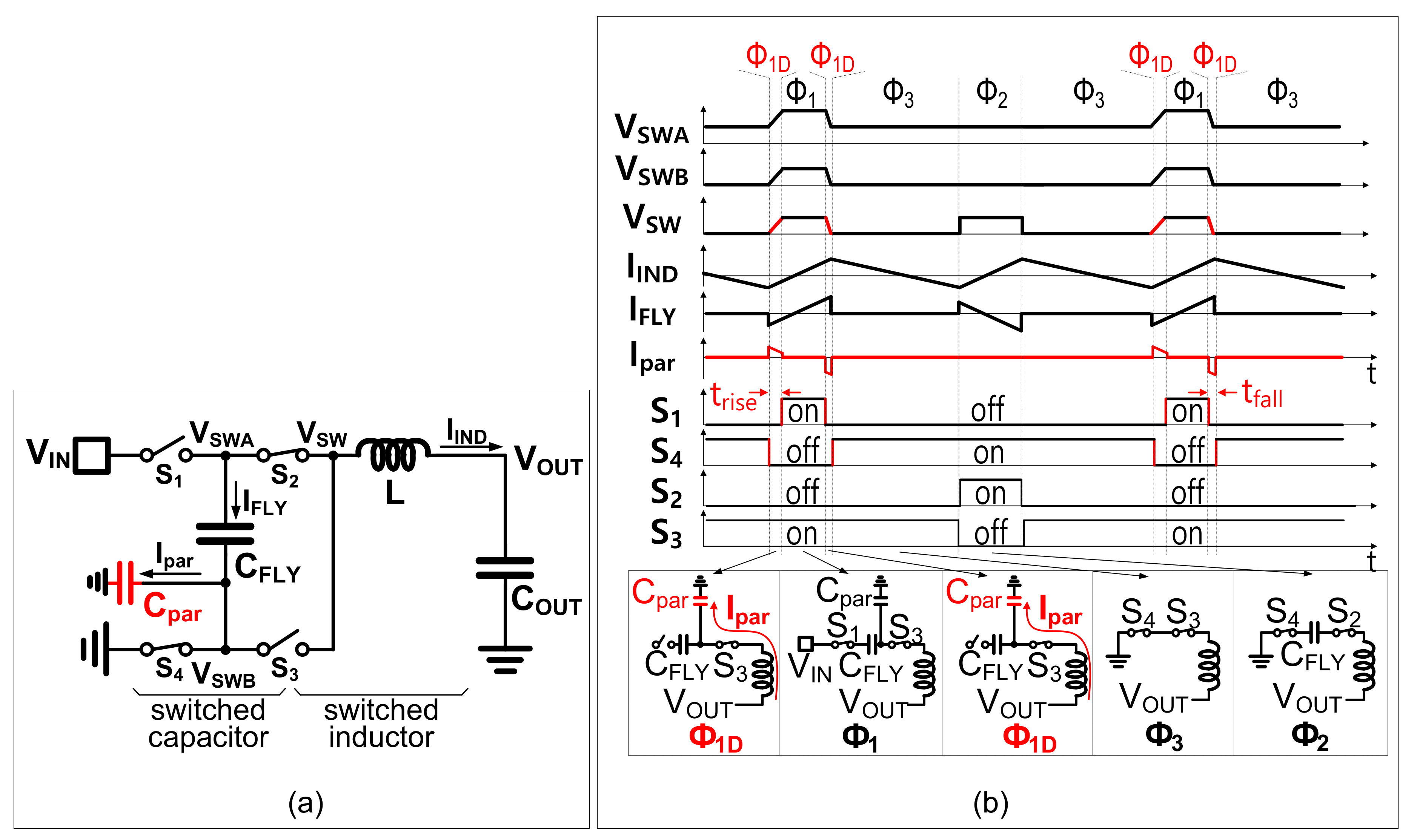
This paper proposes a hybrid DC-DC converter for not only eliminating charge sharing loss and supporting wide-range output voltage but also minimizing the power loss due to Cpar. The proposed soft-switching hybrid DC-DC converter with the 2:1 SC is shown in Figure 2. Without the soft-switching operation, it is also called a 3-level DC-DC converter. With the exception of Φ3 to demagnetize the inductor, the operations during Φ1 and Φ2 are the same as the operations of the conventional 2:1 SC, while Φ1D is added for soft-switching operation. Additional current Ipar is required to charge and discharge Cpar during Φ1D, like the conventional 2:1 SC DC-DC converter. However, thanks to the resonant operation between Cpar and the inductor, L, Ipar flows from the inductor, and not the input while charging Cpar. Also, Ipar flows to the inductor not ground while discharging Cpar. As a result, the power loss due to Cpar can be eliminated if two conditions are met: (1) the inductor current is positive during Φ1D before Φ1 to charge Cpar, and negative during Φ1D after Φ1 to discharge Cpar, and (2) switches are turned on when the drain-to-source voltage is zero. With these conditions, Cpar can be resonantly charged and discharged by the inductor current without power loss. As a result, if a small inductor to increase the inductor-current ripple and a high-accurate soft-switching timing generator for Φ1D are employed, the hybrid DC-DC converters implemented in a standard CMOS process can improve the power efficiency significantly.

3. Proposed Soft-Switching Hybrid DC-DC Converter with 2-phase Switched Capacitor

As shown in Figure 2b, VSWB connected to Cpar does not vary during Φ2, unlike Φ1. To charge and discharge Cpar, the voltage slew of VSW during Φ1D is slower than during Φ2, and the voltage slew depends on the capacitance of Cpar and the amount of Ipar. It makes a difference between the pulse widths during Φ1 and Φ2. Therefore, since the flying capacitor is discharged during Φ2 and charged during Φ1, the amount of charging current can be different from the amount of discharging current. As a result, the voltage of CFLY is varied to equalize the amounts of charging and discharging currents for charge balance, resulting in making CFLY voltage imbalance. The voltage imbalance of CFLY causes a larger output-voltage ripple and lower power-conversion efficiency [16]. To minimize the voltage imbalance of CFLY, this work employs the 2-phase SC topology as illustrated in Figure 3. The SC circuits basically operate with 2 steps for charging and discharging CFLY. Therefore, as depicted in Figure 3a, the proposed 2-phase SC is implemented so that the flying capacitor of SC-PHASE1, CFLY1, is charging/discharging when the flying capacitor of SC-PHASE2, CFLY2, is discharging/charging. The overall operation is the same as the previous 1-phase SC. However, with the 2-phase SC, each capacitor is charged or discharged simultaneously when the inductor is magnetized as shown in Figure 3b. Therefore, half of Cpar always affects all switching events. Moreover, the 2-phase SC keeps the same resonance value of L and 1/2·Cpar for every soft-switching operation, so the periods of Φ1D and Φ2D become the same. As a result, the amounts of charging and discharging currents for the flying capacitors can be the same. The proposed 2-phase SC therefore minimizes the voltage imbalance while the soft-switching technique improves power efficiency. In this work, since the capacitors and switches are fully integrated, the flying capacitor and power transistors can be easily divided in half without additional area and cost.

4. Soft-Switching Timing Generation

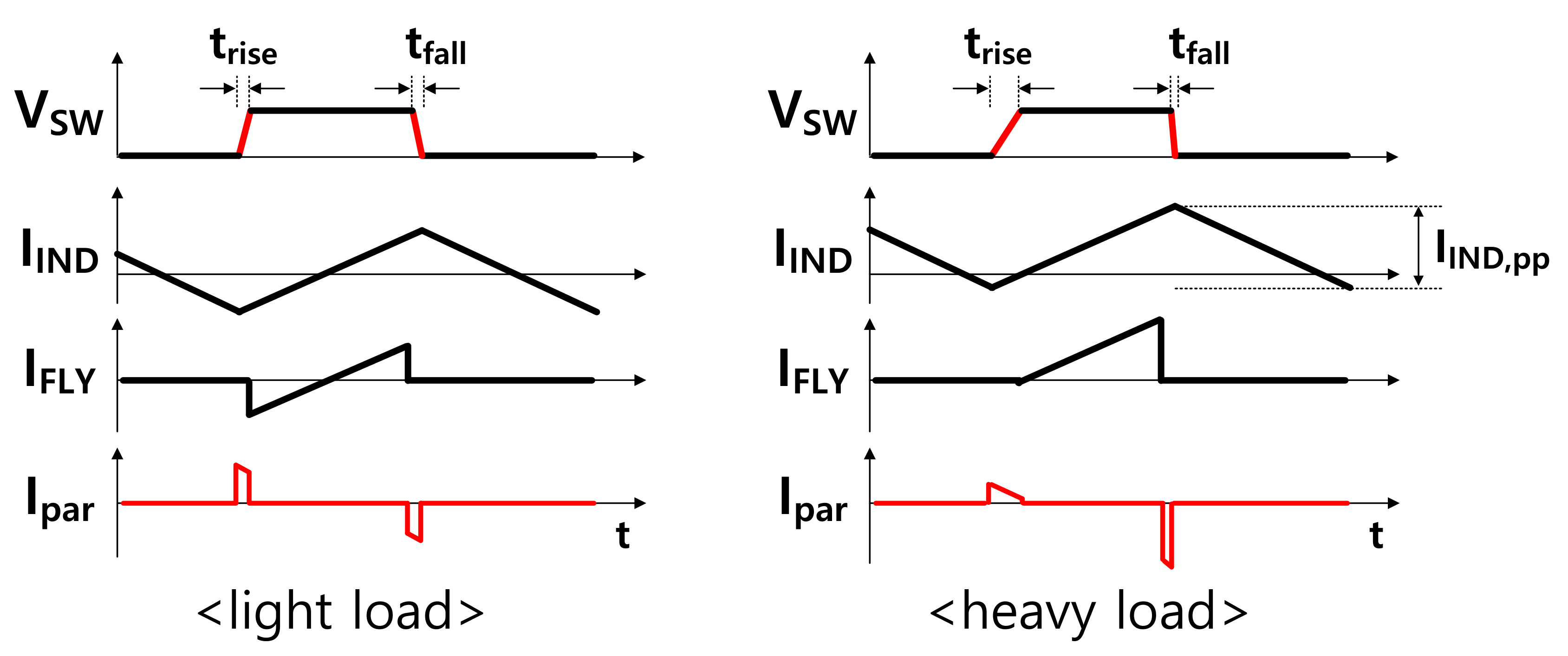
In order to support the proposed soft-switching operation as discussed in Section 2 and Section 3, the accurate timing generations for Φ1D and Φ2D are required. As illustrated in Figure 4, the periods of Φ1D and Φ2D are decided by the rising time, trise, and falling time, tfall, of VSW, and trise and tfall are determined as follows:
t r i s e C p a r , t o t · V I N 2 / ( I L O A D I I N D , p p 2 )
t f a l l C p a r , t o t · V I N 2 / ( I L O A D + I I N D , p p 2 )
where Cpar,tot is the total parasitic capacitance at VSW during Φ1D and Φ2D, VIN is the input voltage, IIND,pp is the peak-to-peak inductor current during a switching period, and ILOAD is the average load current. Based on Equations (2) and (3), trise and tfall can be varied according to parasitic capacitance, input voltage, inductor value, switching frequency of the converter, and load current. So, predetermined delay circuits for Φ1D and Φ2D are difficult to generate accurate timing. Accurate switching-node voltage sensors to determine the exact timing and high-speed gate drivers to turn on the switches immediately are therefore required.
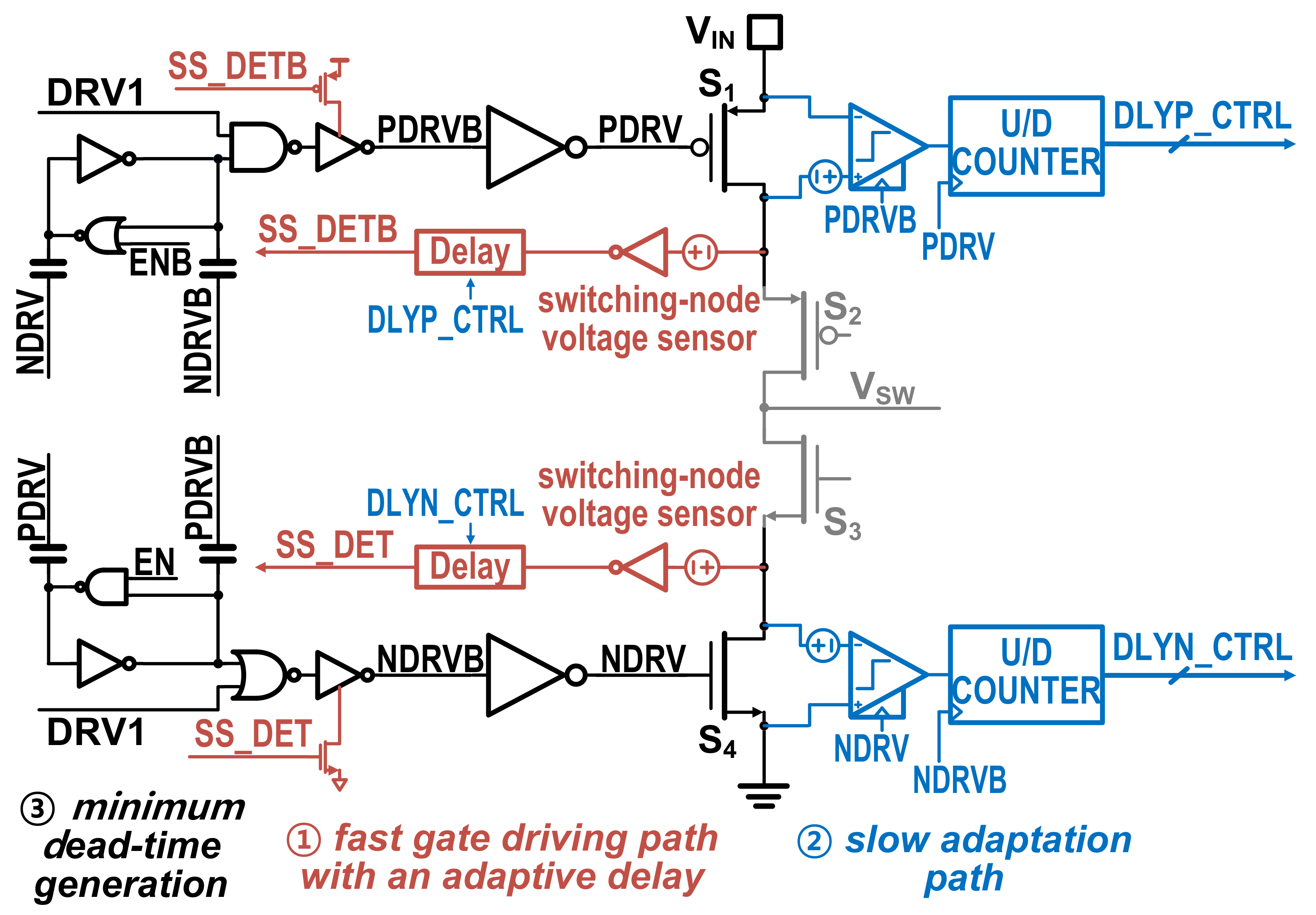
In this work, the adaptive delay generator with the switching-node voltage sensor is implemented to generate an accurate timing for Φ1D and Φ2D, as shown in Figure 5. Since the FIVR in this work should support a high-frequency operation of hundreds of MHz, the delays of the switching-node voltage sensor and the gate driver cannot be ignored for the variations of trise and tfall, resulting in degrading the timing accuracy and, consequently, degrading the power-conversion efficiency. However, the high-speed and high-accurate voltage sensor to support a high-frequency operation requires a large power. Moreover, the gate-driver delay is generally determined by the process and the output-transistor size, not by design. Therefore, instead of using a high-speed and high-accurate voltage sensor, this work adjusts the delay from the voltage sensor to the gate driver using the digital-adaptation loop as shown by the red line in Figure 5. The offset voltage is added to the input of the switching-node voltage sensor to detect the voltage lower or higher than the target, resulting in compensating the gate-driver delay. As shown by the blue line in Figure 5, in every switching cycle, the clocked comparator measures the voltage across the switch to determine whether the switch is turned on at the correct timing, while the up-down counters control the delay codes, DLYP_CTRL and DLYN_CTRL, to adjust the delays of the voltage sensing paths. The high-speed capacitive level shifter is used to generate the minimum dead time between the high-side switch and the low-side switch for reliable operation. The minimum dead time and minimum delay of the voltage sensor are designed to take into account the minimum trise and tfall, according to the load current range.

5. Overall Circuit Implementation and Simulation Results

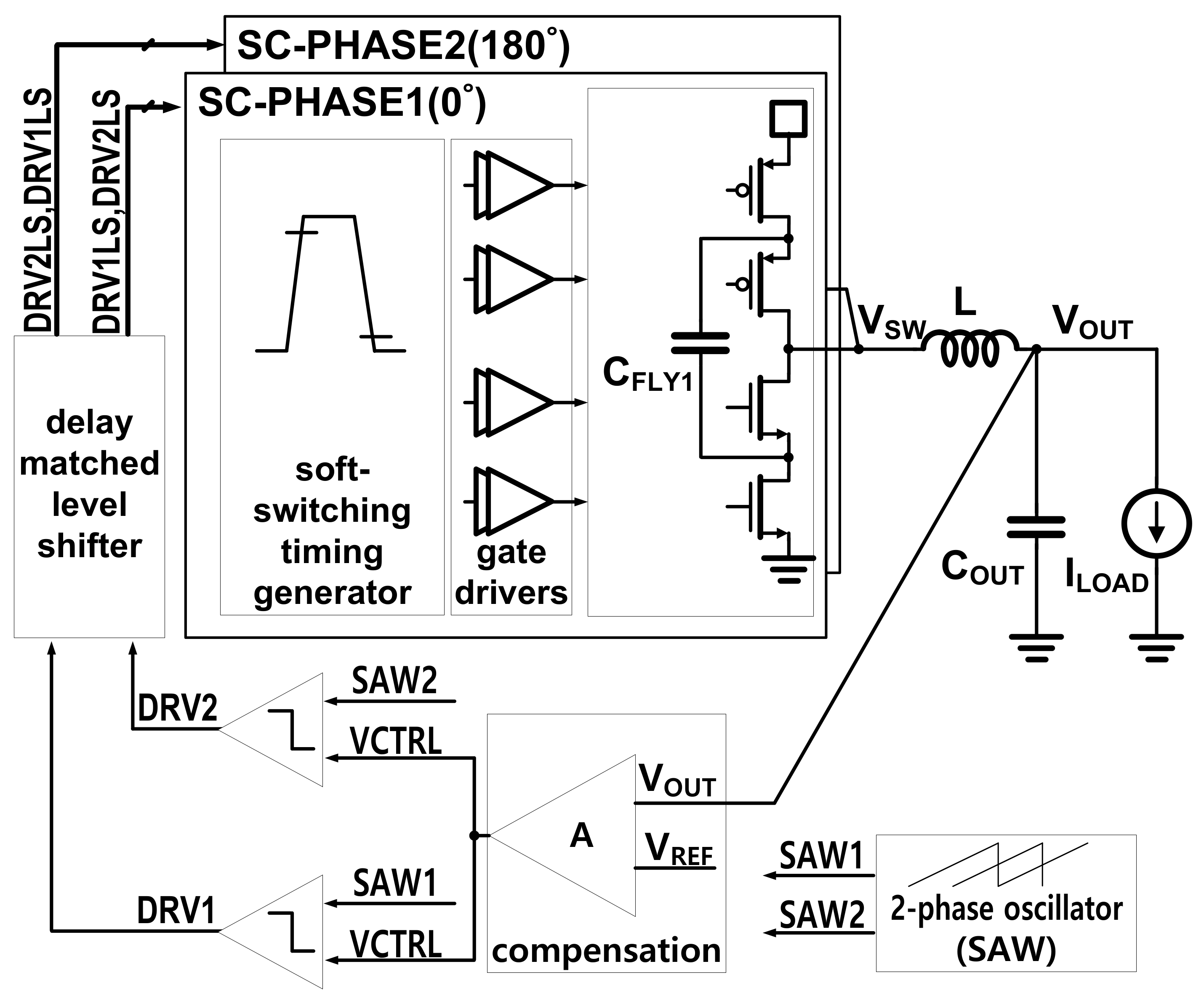
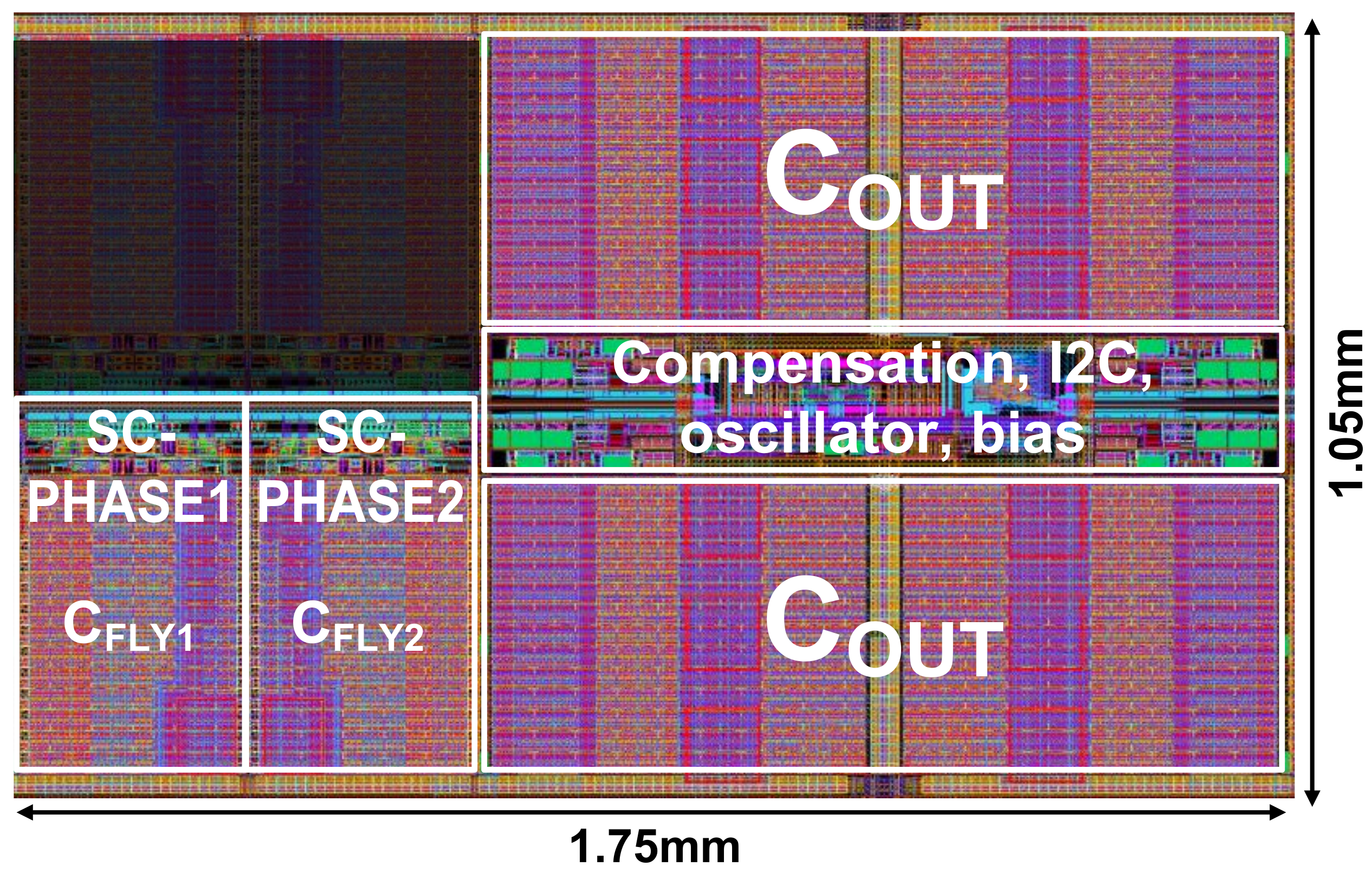
The overall implementation of the proposed soft-switching DC-DC converter with the 2-phase 2:1 SC is shown in Figure 6. The converter is implemented in a 65 nm standard CMOS process and all capacitors are designed with MOS and MOM capacitors. The layout of the converter is shown in Figure 7. The converter is designed with two flying capacitors of 1 nF each and an inductor of 0.8 nH, taking into account package inductors such as bond wires and redistribution layers. The capacitances of the flying capacitors and the parasitic capacitors of the flying capacitors are extracted by post-layout simulation. An amplifier with type-Ⅲ compensation and two sawtooth signals with a 180° phase shift are used for closed-loop control. By applying the two input signals (DRV1LS and DRV2LS) in reverse, the operation of the 2-phase SC is easily implemented. Output transistors are implemented with 1.2 V transistors instead of thick gate transistors with a breakdown voltage of 2.4 V or more, thanks to the advantage of the hybrid architecture.
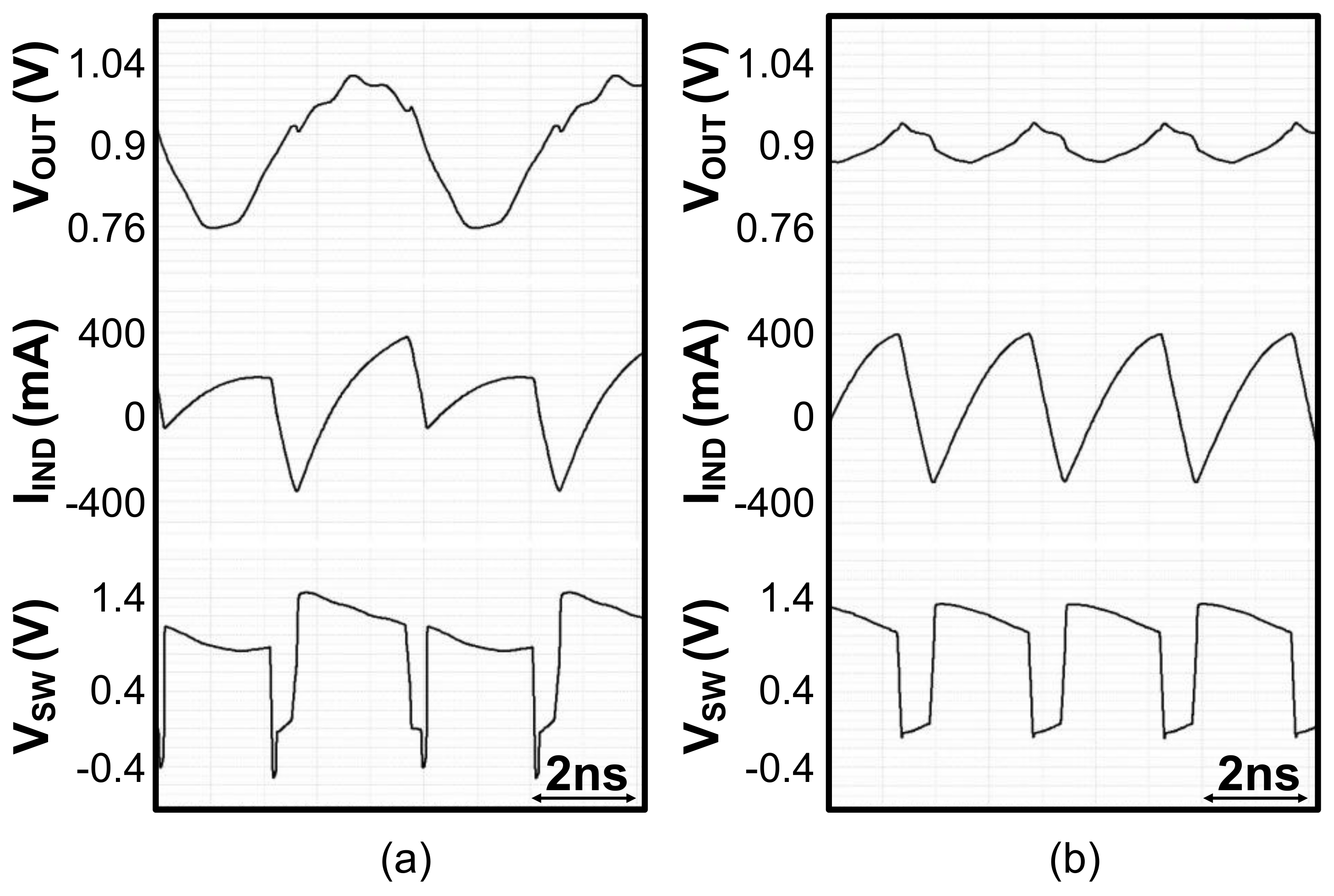
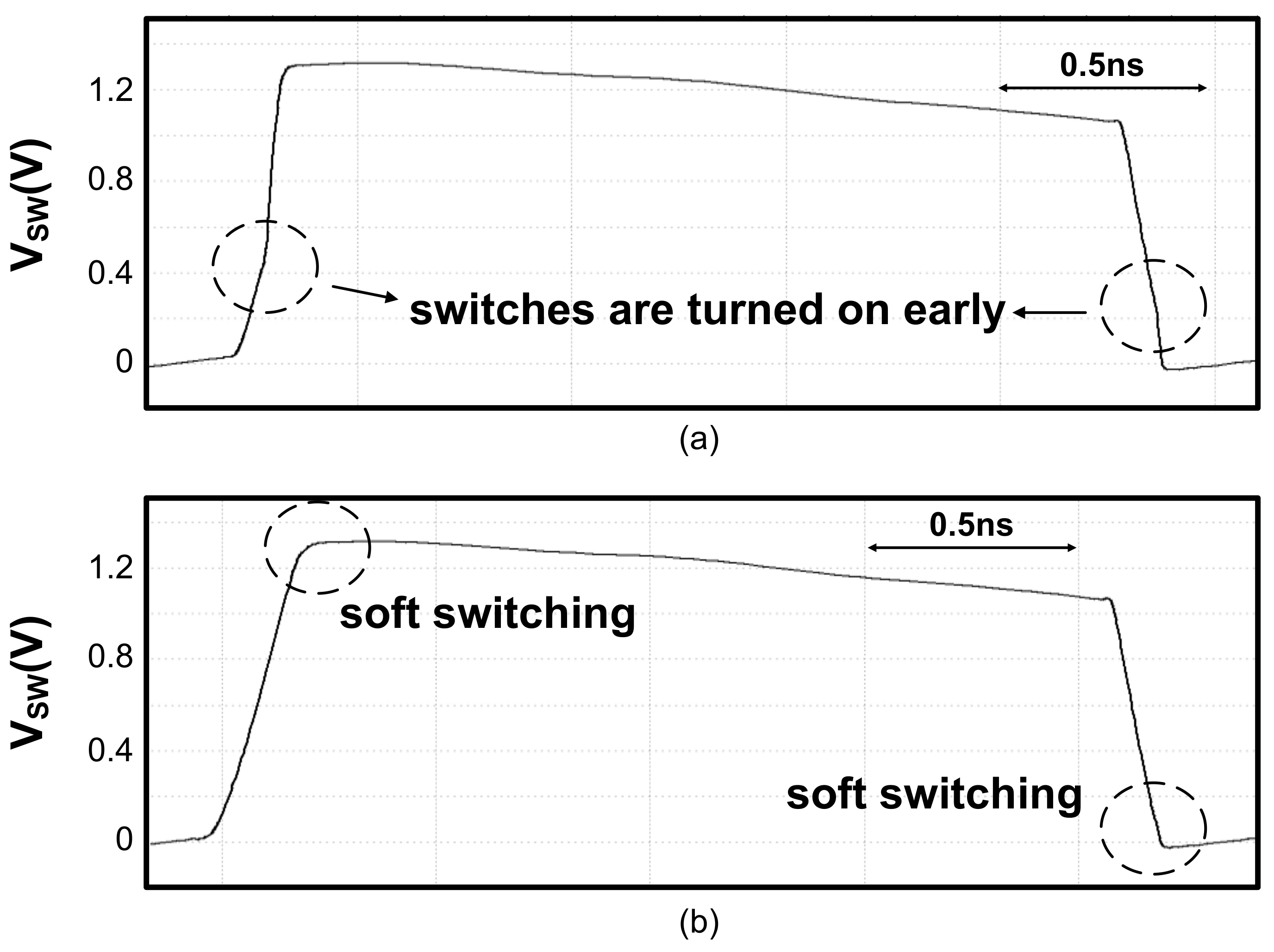
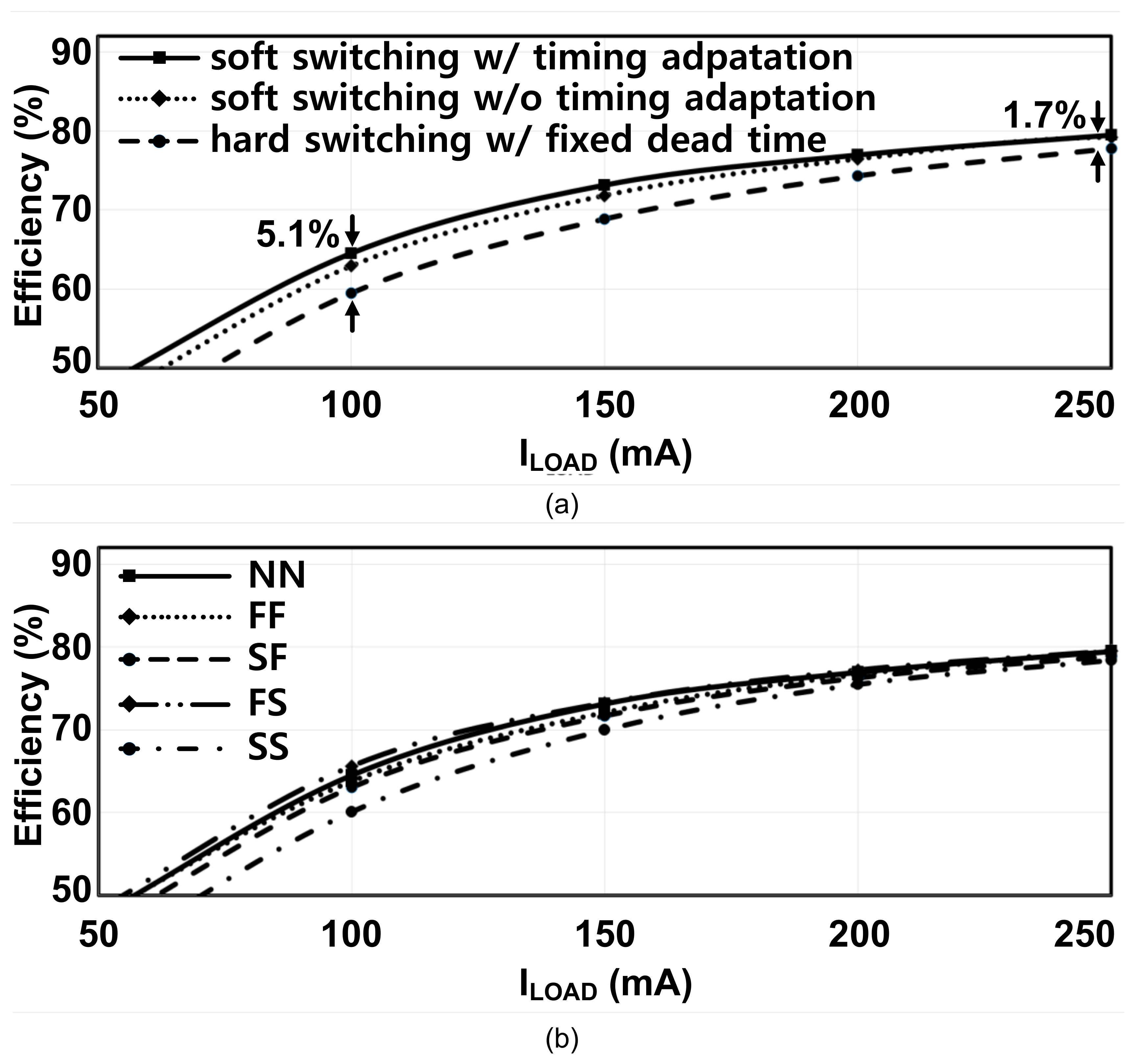
The effects of the proposed 2-phase SC are verified by transistor-based post-layout simulation as shown in Figure 8. With the 2-phase SC, the proposed soft-switching hybrid DC-DC converter maintains the voltage of CFLY at 1/2·VIN regardless of the parasitic capacitance of the flying capacitor. As a result, it prevents the output oscillation and reduces the voltage ripple to about 25% while voltage stresses on switch transistors maintain 1/2·VIN. The proposed soft-switching timing generator is verified, as illustrated in Figure 9. The proposed timing generator turns on the switches at the correct timing, so it supports complete soft-switching operation under any conditions. The power-conversion efficiency is summarized in Figure 10. The proposed soft-switching DC-DC converter with the 2-phase SC improves efficiency by up to 5.1% at 100 mA load current and 1.7% at 250 mA load current. Furthermore, the proposed converter shows a peak efficiency of 78.4% to 79.5% based on five corner simulations.
Table 1 compares the performance of the proposed converter with other FIVRs. Although the buck converter in [3] supports a wide range of the output from 0.45 V to 1.05 V, the converter shows a low peak efficiency of 71% and requires an inductor of 11.8 nH. The SC DC-DC converter in [14] shows a high peak efficiency of 82%, however, the maximum current is 100 mA and supports only a 3:1 conversion ratio, so the input and output ranges are limited. The hybrid DC-DC converter with a small inductor of 1.5 nH in [11] supports a low input voltage of 1.5 V and achieves a low peak efficiency of 72%. Another hybrid DC-DC converter implemented in 28 nm FDSOI process in [2] can support a high input voltage of 4.2 V and shows a high peak efficiency of 78%. However, the converter provides a low output current of about 33 mA and requires an inductor of 3 nH and two flying capacitors of 5 nF each.
Compared with these previous works, the proposed DC-DC converter is implemented with the smallest inductor of 0.8 nH and flying capacitors totaling 2 nF. The proposed soft-switching architecture allows the use of a small inductor and a low switching frequency with low power losses, resulting in supporting a high load current of 250 mA. Furthermore, the proposed hybrid DC-DC converter minimizes power losses due to the parasitic capacitance of the flying capacitors in a standard CMOS process. As a result, the converter achieves a high peak efficiency of 79.5%. The proposed converter provides a wide range of outputs from 0.4 V to 1.2 V with an input voltage from 2.0 V to 2.4 V to support DVFS of digital processors, which is typically required for FIVRs.

6. Conclusions

The fully-integrated soft-switching hybrid DC-DC converter is proposed to minimize the power loss due to the parasitic capacitance of the flying capacitors. Although the 2:1 SC was used in this work, the other SC topologies such as Dickson, flying capacitor multilevel, etc. can be implemented with the proposed schemes to improve power-conversion efficiency. The proposed 2-phase SC topology sufficiently reduces the voltage imbalance of the flying capacitor without additional area. The proposed DC-DC converter using the flying capacitor in a standard CMOS process achieves a high peak efficiency of 79.5%, and the proposed soft-switching scheme with the adaptive timing generator improves efficiency by up to 5.1%.

Author Contributions

Conceptualization, M.C.; Investigation, M.C.; Visualization, M.C.; Writing-review & editing, D.-K.J.; Supervision, D.-K.J. All authors have read and agreed to the published version of the manuscript.

Funding

This research received no external funding.

Conflicts of Interest

The authors declare no conflict of interest.

References

  1. Gutierrez, F. Fully-Integrated Converter for Low-Cost and Low-Size Power Supply in Internet-of-Things Applications. Electronics 2017, 6. [Google Scholar] [CrossRef] [Green Version]
  2. Amin, S.S.; Mercier, P.P. A Fully Integrated Li-Ion-Compatible Hybrid Four-Level DC–DC Converter in 28-nm FDSOI. IEEE J. Solid-State Circuits 2019, 54, 720–732. [Google Scholar] [CrossRef]
  3. Kar, M.; Singh, A.; Rajan, A.; De, V.; Mukhopadhyay, S. An All-Digital Fully Integrated Inductive Buck Regulator With A 250-MHz Multi-Sampled Compensator and a Lightweight Auto-Tuner in 130-nm CMOS. IEEE J. Solid-State Circuits 2017, 52, 1825–1835. [Google Scholar] [CrossRef]
  4. Lee, M.; Choi, Y.; Kim, J. A 500-MHz, 0.76-W/mm Power Density and 76.2% Power Efficiency, Fully Integrated Digital Buck Converter in 65-nm CMOS. IEEE Trans. Ind. Appl. 2016, 52, 3315–3323. [Google Scholar] [CrossRef]
  5. Wang, W.-L.; Lin, H.; Yu, C.-L.; Henrickson, L.E. Output current enhanced cyclic switched-capacitor step-down DC–DC regulator. Electron. Lett. 2018, 54, 95–97. [Google Scholar] [CrossRef]
  6. Villar-Piqué, G.; Bergveld, H.J.; Alarcón, E. Survey and Benchmark of Fully Integrated Switching Power Converters: Switched-Capacitor Versus Inductive Approach. IEEE Trans. Power Electron. 2013, 28, 4156–4167. [Google Scholar] [CrossRef] [Green Version]
  7. Lee, J.-Y.; Kim, G.-S.; Oh, K.-I.; Baek, D. Fully Integrated Low-Ripple Switched-Capacitor DC–DC Converter with Parallel Low-Dropout Regulator. Electronics 2019, 8, 98. [Google Scholar] [CrossRef] [Green Version]
  8. Jung, W.; Sylvester, D.; Blaauw, D. A rational-conversion-ratio switched-capacitor DC-DC converter using negative-output feedback. In Proceedings of the 2016 IEEE International Solid-State Circuits Conference (ISSCC), San Francisco, CA, USA, 31 January–4 February 2016; pp. 218–219. [Google Scholar] [CrossRef] [Green Version]
  9. Teh, C.K.; Suzuki, A. A 2-output step-up/step-down switched-capacitor DC-DC converter with 95.8% peak efficiency and 0.85-to-3.6V input voltage range. In Proceedings of the 2016 IEEE International Solid-State Circuits Conference (ISSCC), San Francisco, CA, USA, 31 January–4 February 2016; pp. 222–223. [Google Scholar] [CrossRef]
  10. Lei, Y.; Pilawa-Podgurski, R.C.N. A General Method for Analyzing Resonant and Soft-Charging Operation of Switched-Capacitor Converters. IEEE Trans. Power Electron. 2015, 30, 5650–5664. [Google Scholar] [CrossRef]
  11. Kumar, P.; Vaidya, V.A.; Krishnamurthy, H.; Kim, S.; Matthew, G.E.; Weng, S.; Thiruvengadam, B.; Proefrock, W.; Ravichandran, K.; De, V. A 0.4V~1V 0.2A/mm2 70% efficient 500MHz fully integrated digitally controlled 3-level buck voltage regulator with on-die high density MIM capacitor in 22nm tri-gate CMOS. In Proceedings of the 2015 IEEE Custom Integrated Circuits Conference (CICC), San Jose, CA, USA, 28–30 September 2015. [Google Scholar] [CrossRef]
  12. Zucchelli, M.; Colalongo, L.; Richelli, A.; Kovacs-Vajna, Z.M. Dickson charge pump using integrated inductors in complementary metal–oxide semiconductor technology. Iet Power Electron. 2016, 9, 553–558. [Google Scholar] [CrossRef]
  13. Mahmoudidaryan, P.; Mandal, D.; Bakkaloglu, B.; Kiaei, S. Wideband Hybrid Envelope Tracking Modulator With Hysteretic-Controlled Three-Level Switching Converter and Slew-Rate Enhanced Linear Amplifier. IEEE J. Solid-State Circuits 2019, 54, 3336–3347. [Google Scholar] [CrossRef]
  14. Butzen, N.; Steyaert, M. 10.1 A 1.1W/mm2-power-density 82%-efficiency fully integrated 3∶1 Switched-Capacitor DC-DC converter in baseline 28nm CMOS using Stage Outphasing and Multiphase Soft-Charging. In Proceedings of the 2017 IEEE International Solid-State Circuits Conference (ISSCC), San Francisco, CA, USA, 5–9 February 2017; pp. 178–179. [Google Scholar] [CrossRef] [Green Version]
  15. Butzen, N.; Steyaert, M. A 94.6%-efficiency fully integrated switched-capacitor DC-DC converter in baseline 40nm CMOS using scalable parasitic charge redistribution. In Proceedings of the 2016 IEEE International Solid-State Circuits Conference (ISSCC), San Francisco, CA, USA, 31 January–4 February 2016; pp. 220–221. [Google Scholar] [CrossRef] [Green Version]
  16. Liu, X.; Huang, C.; Mok, P.K.T. A 50MHz 5V 3W 90% efficiency 3-level buck converter with real-time calibration and wide output range for fast-DVS in 65nm CMOS. In Proceedings of the 2016 IEEE Symposium on VLSI Circuits (VLSI-Circuits), Honolulu, HI, USA, 13–17 June 2016. [Google Scholar] [CrossRef]
Figure 1. 2:1 SC DC-DC converter with the parasitic capacitor of a flying capacitor, CFLY.
Electronics 09 00372 g001
Figure 2. Soft-switching hybrid DC-DC converter with the 2:1 SC: (a) block diagram (b) timing diagram when VOUT < 1/2·VIN.
Electronics 09 00372 g002
Figure 3. Proposed soft-switching hybrid DC-DC converter with the 2-phase 2:1 SC: (a) block diagram (b) timing diagram when VOUT < 1/2·VIN.
Electronics 09 00372 g003
Figure 4. Waveforms and timing variation of trise and tfall according to the load currents.
Electronics 09 00372 g004
Figure 5. Circuit implementations of soft-switching timing generator for S1 and S4 with minimum dead time, gate drivers, and output power transistors.
Electronics 09 00372 g005
Figure 6. Overall implementation of the proposed soft-switching hybrid DC-DC converter.
Electronics 09 00372 g006
Figure 7. Chip layout of the proposed DC-DC converter.
Electronics 09 00372 g007
Figure 8. Simulated waveforms of the soft-switching hybrid DC-DC converter in steady state: (a) with the conventional 1-phase SC and (b) with the proposed 2-phase SC.
Electronics 09 00372 g008
Figure 9. Switching-node waveforms (a) without the adaptive timing generation and (b) with the adaptive timing generation.
Electronics 09 00372 g009
Figure 10. Power-conversion efficiency (a) according to the output current and (b) process corners at VIN = 2.4 V and VOU T= 1.0 V.
Electronics 09 00372 g010
Table 1. Performance comparison of different FIVRs (fully integrated voltage regulators).
[3][14][11][2]This Work
StructureBuckSCHybridHybridHybrid
Process130 nm CMOS28 nm CMOS22 nm CMOS28 nm FDSOI65 nm CMOS
VIN [V]1.23.21.52.8–4.22.0–2.4
VOUT [V]0.45–1.050.950.4–1.20.6–1.20.4–1.2
IMAX [A]0.070.1 *0.150.033 *0.25
L [nH]11.8-1.530.8
CFLY [nF]-1.555 (×2)2
FSW [MHz]125/2501600500200340
Peak efficiency [%]7182727879.5
Area [mm2]1.190.1171.51.51.5
VeificationMeasuredMeasuredMeasuredMeasuredSimulated
* estimated from the paper.