Wide Voltage Resonant Converter Using a Variable Winding Turns Ratio

Department of Electrical Engineering, National Yunlin University of Science and Technology, Yunlin 640, Taiwan
*
Author to whom correspondence should be addressed.
Electronics 2020, 9(2), 370; https://doi.org/10.3390/electronics9020370
Submission received: 5 February 2020
/
Revised: 18 February 2020
/
Accepted: 20 February 2020
/
Published: 21 February 2020
(This article belongs to the Section Power Electronics)
Abstract
:This paper presents a inductor–inductor–capacitor (LLC) resonant converter with variable winding turns to achieve wide voltage operation (100–400 V) and realize soft switching operation over the entire load range. Resonant converters have been developed for consumer power units in computers, power servers, medical equipment, and adaptors due to the advantages of less switching loss and better circuit efficiency. The main disadvantages of the LLC resonant converter are narrow voltage range operation owing to wide switching frequency variation and limited voltage gain. For computer power supplies with hold-up time function, electric vehicle battery chargers, and for power conversion in solar panels, wide input voltage or wide output voltage operation capability is normally demanded for powered electronics. To meet these requirements, the variable winding turns are used in the presented circuit to achieve high- or low-voltage gain when Vin is at low- or high-voltage, respectively. Therefore, the wide voltage operation capability can be implemented in the presented resonant circuit. The variable winding turns are controlled by an alternating current (AC) power switch with two back-to-back metal-oxide-semiconductor field-effect transistors (MOSFETs). A 500-W prototype is implemented and test results are presented to confirm the converter performance.
1. Introduction
Renewable energy systems with electronic power techniques [1,2,3,4] have been widely researched to lessen the demands for fossil fuels and reduce the effects of global warming. Form the various renewable energy sources, solar and wind power are more attractive out of the clean energy sources. The main problem with solar and wind power is the non-constant output voltage from wind turbine generators and photovoltaic (PV) solar panels. The output voltage of a wind turbine generator is related to wind speed and the output voltage of a PV solar panel is related to solar intensity. High-efficiency direct current (DC) power converters [5,6,7,8] have been proposed for power units for computers, battery dischargers and chargers, telecommunication systems, and server systems. Out of the various soft switching techniques, the active clamp technique [9,10], asymmetric pulse width modulation (PWM) [11,12], and phase-shift PWM converters [13,14] are the most attractive circuit topologies with the lowest switching losses. The PWM scheme is widely used to control these circuit topologies with constant output voltage. However, the turn-on time of the PWM scheme is dependent on the input voltage. PWM converters have a low (high) duty cycle at high (low) voltage input. However, the low duty cycle results in a high root mean square current and high conduction loss. Thus, the PWM converters have low (high) circuit efficiency at high (low) input voltage conditions. This drawback limits PWM converters in terms of wide voltage operation. Pulse frequency modulation (PFM), or variable frequency control, has been adopted in resonant converters [15]. In many resonant circuit topologies, the inductor–inductor–capacitor (LLC) resonant converter is a more attractive circuit topology for use in high-input voltage inputs. The main advantages of LLC resonant converters [16,17,18] are low switching loss in power devices, high efficiency, and low electromagnetic interference (EMI). The main drawback of LLC resonant converters is the limited voltage gain. This means it is difficult to operate the resonant converter in wide voltage operation. To realize wide voltage operation, two-stage converters and series–parallel connection for full-bridge or half-bridge converters [19,20,21,22] have been proposed for battery charger, solar power, and wind power applications. The two-stage converters have the drawback of low efficiency, while the series- or parallel-connected converters have more circuit components, which increase the conduction loss and reduce the converter reliability. In [23,24], two full-bridge LLC converters with primary-parallel–secondary-series connection were proposed to achieve wide input or output voltage operation. However, eight power switches and eight diodes are used in this circuit topology. The conduction losses in power semiconductors and the cost are increased. An interleaved LLC resonant converter has been studied and implemented in [25] to realize wide input voltage operation and ripple-free input current. However, this circuit topology is a two-stage circuit structure, meaning that the circuit efficiency is low in full load conditions, when both the boost converter and LLC converter are operated. In [26], a half-bridge LLC resonant converter with two sets of center-tapped rectifiers was proposed to extend the hold-up time problem for personal computers. However, four winding turns are used on the secondary side in this circuit topology, and the copper losses on magnetic windings are increased.
An LLC resonant converter with variable winding turns is proposed and investigated to achieve soft switching operation on active switches over the entire load range and for wide voltage range operation (Vin = 100–400 V). The variable winding turns controlled by an alternating current (AC) switch are adopted to achieve different voltage gains based on low- or high-input voltage ranges. During the low-input voltage range (from Vin = 100 V to 200 V), the converter with more secondary turns is selected to achieve high-voltage gain for the LLC converter. During the input voltage range (Vin = 200–400 V), the converter with fewer secondary turns is operated to achieve low-voltage gain for the LLC converter. Therefore, the proposed converter can be operated under wide input voltage variation, such as for solar power or switching mode power supplies without power factor correction, under the universal AC input voltage. The LLC resonant circuit with pulse-frequency modulation is used to control active devices. Due to the inductive impedance load of the LLC resonant tank, the converter can realize soft switching operation for both active switches and rectifier diodes. The voltage double rectifier topology is adopted on the output side to limit the voltage rating of the secondary diodes at Vo instead of 2Vo in center-tapped rectifiers. The rectifier diodes with a low-voltage rating have low-voltage drop. Comparing the center-tapped rectifier structure, the voltage double rectifier structure has less conduction losses for rectifier diodes and secondary windings. Comparing the conventional two-stage power converters, parallel-series connected converters, and the other resonant converters in [19,20,21,22,23,24,25,26], the presented LLC resonant converter has a simple circuit structure, a simple control algorithm, and requires fewer power components to achieve wide voltage operation. The description of the presented circuit schematic and operation principle is presented in Section 2. The circuit analysis and design procedures of the presented resonant converter are provided in Section 3. Experiments are demonstrated and discussed to confirm the effectiveness of the presented converter in Section 4. Finally, the conclusions are discussed in Section 5.
2. Proposed Converter and Operation Principle
Figure 1a shows the conventional LLC converter. The half-bridge leg and center-tapped rectifier are used on the primary and secondary sides, respectively, for high-voltage input and low-voltage output applications. According to the center-tapped rectifier topology, the secondary diodes have 2Vo voltage stress. Figure 1b shows the circuit topology with the voltage double rectifier for medium- or high-voltage output applications. The advantages of this circuit topology are the low-voltage rating of the rectifier diodes (VD1,rating = VD1,rating = Vo) and fewer secondary winding turns (ns instead of 2ns) in the center-tapped rectifier structure. Therefore, the voltage double rectifier structure has less copper loss on the secondary windings.
In order to improve the drawback of the limit voltage range in conventional LLC converters, Figure 2a shows the circuit configuration of the presented LLC converter with variable winding turns to achieve wide input voltage operation (100–400 V). The input voltage of the proposed LLC converter can be from the output of the solar panels, wind turbine DC generators, or battery banks. The output voltages of battery banks and large solar panels vary widely. A half-bridge LLC resonant tank is used on the primary side for soft switching operation in active devices S1 and S2 over the entire load range. The voltage rating of the active devices equals the maximum input voltage. Two sets of voltage double rectifiers and one AC switch Sac implemented with two metal-oxide-semiconductor field-effect transistors (MOSFETs) back-to-back connection are used on the output-side. If the proposed converter is operated under low-voltage input Vin,L (100–200 V), then Sac is turned on (Figure 2b). Due to Sac is conducting, the 2ns secondary winding turns are connected to load voltage. One observes that D3 and D4 are off. The transformer turns-ratio under low-input voltage operation is np/(2ns). The proposed converter has DC voltage gain Vo/Vin,L = G(f)(2ns)/np, where Vin,L and G (f) are low-input voltage range and the voltage transfer function of LLC converter. When the circuit is worked under high-voltage range Vin,H (200–400 V), Sac is controlled at off state (Figure 2c). The ns winding turns are connected to load voltage and the diodes D1 and D2 are off. Therefore, the transformer turns-ratio for high-voltage operation is equal to np/ns. The direct current voltage gain Vo/Vin,H of the LLC converter is G(f)ns/np, where Vin,H is high-input voltage range. From the previous discussion, one can observe that Vo/Vin,L = G(f)(2ns)/np = 2Vo/Vin,H. It is concluded that Vin,H = 2Vin,L, such as Vin,H = 200–400 V and Vin,L = 100–200 V. Therefore, the presented resonant converter has high (low) DC voltage gain operated at low (high) input voltage range with low (high) transformer turns-ratio. The PWM signals of S1 and S2 are controlled with pulse-frequency modulation scheme shown in Figure 3a and Figure 4a and the AC switch Sac is controlled by the Schmitt voltage comparator. The reference voltage of the Schmitt voltage comparator is 200 V and the hysteresis voltage band is 10 V.
2.1. Low-Voltage Operation Vin,L = Vin,min–2Vin,min (Sac: on, D3, D4: off)
If the converter is operated at the low-voltage input from Vin,min to 2Vin,min, then Sac is turned on and D3 and D4 are turned off. The proposed converter has a DC voltage gain of Vo/Vin,L = G(f)(2ns)/np. According to the switching states of S1, S2, D1, and D2, the converter has six operating modes for each switching cycle. The PWM waveforms are demonstrated in Figure 3a. Figure 3b–g gives the equivalent circuits of six operating modes under fr1 (series resonant frequency) > fsw (switching frequency).
Mode 1 [t0 ~ t1]: This mode begins at t0 if vCS1 = 0 V and vCS2 = Vin. Owing to iLr(t0) < 0 and iLr > iLm, the body diode DS1 conducts and D1 is forward-biased. Switch S1 turns on after t0 to achieve zero voltage switching. The magnetizing voltage vLm = npVCo1/(2ns) = npVo/(4ns) and the magnetizing current iLm increase in this mode. In mode 1, the series resonant frequency is . If fr1 (series resonant frequency) < fsw (switching frequency), then the circuit goes to mode 3. Otherwise, the circuit goes to mode 2 at time t1.
Mode 2 [t1 ~ t2]: At t1, iD1 = 0 and D1 turns off without the reverse recovery current. In mode 2, the resonant frequency is . It is clear that the resonant frequency fr2 in mode 2 is less than the frequency fr1 in mode 1. The peak-to-peak current of Lm is approximately obtained as
Thus, the magnetizing current at time t2 is given as
Mode 3 [t2 ~ t3]: This mode starts at t2 when switch S1 is turned off. Owing to iLr(t2) > 0 and iLr < iLm, CS2 (CS1) is discharged (charged) from Vin (0 V) and D2 is forward-biased. If the inductor energy ELr+Lm at time t2 is larger than the capacitor energy ECS1+CS2, then vCs2 will be decreased to zero voltage at time t3. The zero voltage switching condition of S2 is expressed as
where Coss = CS1 = CS2. The dead time (td) between S1 and S2 must be greater than the discharge time of CS2 to ensure the zero voltage turn-on of S2. Thus, the maximum value of Lm can be calculated as
Mode 4 [t3 ~ t4]: At time t3, vCS2 = 0 V and vCS1 = Vin. Owing to iLr(t3) > 0 and iLr < iLm, the body diode DS2 conducts and D2 is forward-biased. S2 can turn on after t3 with soft switching operation. In mode 4, vLm = −npVCo2/(2ns) = −npVo/(4ns) and iLm decreases. The resonant frequency in mode 4 is fr1. If fsw < fr1, then iD2 = 0 at time t4.
Mode 5 [t4 ~ t5]: At t4, iD2 = 0 and D2 turns off without the reverse recovery current. Lr, Lm, and Cr are naturally resonant with the frequency fr2.
Mode 6 [t5 ~ Tsw+t0]: At t5, S2 is turned off. Owing to iLr(t5) < 0 and iLr > iLm, CS1 is discharged and D1 is forward-biased. The soft switching turn-on condition of S1 is expressed as
At time t0 + Tsw, vCS1 = 0 V.
2.2. High-Voltage Operation Vin,H = 2Vin,min–4Vin,min (Sac: off, D1, D2: off)
If the converter is worked at the high-voltage input from 2Vin,min to 4Vin,min, then Sac turns off, and D1 and D2 are also off. The DC voltage gain becomes Vo/Vin,H = G(f)ns/np. According to the on–off states of S1, S2, D3, and D4, the LLC converter has six operating modes for each switching period. Figure 4 gives the PWM waveforms and equivalent circuits under high-input voltage operation.
Mode 1 [t0 ~ t1]: At time t0, vCS1 = 0 V. Since iLr > iLm and iLr(t0) < 0, DS1 is forward-biased and D3 conducts. Thus, the zero voltage turn-on of S1 can be realized after t0. Due to D3 being forward-biased, one can obtain vLm = npVCo1/ns = npVo/(2ns) and iLm increases. The resonant frequency in mode 1 is .
Mode 2 [t1 ~ t2]: At time t1, iD3 = 0 and D3 turns off at t1 without the reverse recovery current. The resonant frequency in mode 2 is . The peak-to-peak ripple current ΔLm and the magnetizing current at time t2 are approximately calculated as
Mode 3 [t2 ~ t3]: At t2, S1 turns off. Due to iLr < iLm and iLr(t2) > 0, D4 conducts and CS2 is discharged from Vin. If the inductor energy on Lr and Lm is larger than the capacitor energy on CS1 and CS2, then vCS2 is decreased to zero voltage at t3. The zero voltage turn-on condition of S2 is expressed as
If the dead time (td) between S1 and S2 is given, the maximum value of Lm under the high-input voltage range is obtained as
Mode 4 [t3 ~ t4]: At t3, vCS2 = 0. Owing to iLm > iLr and iLr(t3) > 0, D4 conducts and DS2 is forward-biased. Therefore, the zero voltage turn-on of S2 can be achieved. Due to D4 conducting, one can obtain vLm = -npVCo2/ns = -npVo/(2ns) and iLm decreases in this mode. The resonant frequency in this mode is fr1.
Mode 5 [t4 ~ t5]: At time t4, iD4 = 0 and D4 turns off without the reverse recovery current. The resonant frequency in mode 5 equals fr2.
Mode 6 [t5 ~ Tsw+t0]: At time t5, S2 turns off. Since iLm < iLr and iLr(t5) < 0, D3 is forward-biased and CS1 is discharged. The zero voltage turn-on condition of S1 is expressed as
At t0 + Tsw, vCS1 = 0.
3. Circuit Analysis and Design Procedure
The presented LLC converter is operated with pulse frequency modulation (PFM). Power switches have a constant duty cycle (d = 0.5) with variable frequency. The switching frequency is dependent on Vin and Po. The fundamental harmonic frequency approach is used to analyze the circuit characteristics. The variable winding turns controlled by the AC switch Sac are used on the secondary side to adjust the voltage gain under low- or high-voltage input. Based on the fundamental harmonic frequency analysis, the AC equivalent circuit of the resonant tank is given in Figure 5. Re is the equivalent primary side resistor of transformer. Since the PWM signals of S1 and S2 are square waves with duty cycle d = 0.5, the input voltage of the LLC circuit becomes a square voltage wave measuring 0 V (if S2 is on) or Vin (if S1 is on). The fundamental root mean square (rms) input voltage is calculated as . Since Sac is turned on at low-voltage inputs and off at high-voltage inputs, the secondary winding turns 2ns (ns) are connected to the output load under low (high) input voltage ranges. The primary side magnetizing voltage is a square wave with a voltage value of vLm = ±npVo/(4ns) if Sac is conducting or vLm = ±npVo/(2ns) if Sac is off. The fundamental rms voltage VLm,rms is calculated as for low-input voltage ranges or for high-input voltage operation. The DC load resistor Ro is reflected to the primary side of the transformer and the AC equivalent resistor Re can be obtained as for low-voltage ranges or for high-voltage ranges. The voltage transfer function in Figure 5 is calculated as
Here, , Fn = fsw/fr and Ln = Lm/Lr. From Equation (11), the output voltage is obtained as
Power switches S1 and S2 are controlled with pulse frequency modulation and the LLC converter is operated over wide voltage ranges.
The design procedures of prototypes are provided to confirm the feasibility of the presented LLC converter. The input voltage range Vin is from 100 to 400 V, the output voltage Vo is 48 V, the full power Po,rated is 500 W, and the series resonant frequency fr1 is 100 kHz. The inductance ratio Ln is assumed as 7. When Vin = 100–200 V, the proposed converter is operated at low-voltage ranges. If Vin = 200–400 V, then the proposed LLC converter is worked under high-voltage ranges. Since the proposed converter has the same resonant tank under high and low-voltage ranges, the prototype circuit can be designed for either high- or low-input voltage ranges. For high-voltage range operation, the minimum voltage gain of the presented LLC converter under Vin,max = 400 V is assumed at unity. Then, the turns ratio np/ns is expressed in Equation (13) as
The magnetic core TDK EE-55 with ΔB = 0.4 T and Ae = 354 mm2 is adopted to implement transformer T. It is assumed that the minimum switching frequency is 50 kHz under Vin = 200 V conditions. Therefore, the minimum primary winding turns are calculated as
In the laboratory prototype, we selected np = 16 and ns = 2. Thus, the actual DC gains are obtained in Equations (15) and (16) as
Similarly, the DC voltage gains of the presented resonant converter for low-voltage ranges are obtained as
From the calculated winding turns np and ns, the equivalent resistance Re at high-voltage ranges and the rated power are calculated as
The quality factor X is selected as 0.2. The resonant inductor Lr is calculated as
In the proposed converter, the actual resonant inductance Lr is 20 μH. Then, the resonant capacitor is calculated as
Since the selected Ln = Lm/Lr = 7, the magnetizing inductance Lm is obtained as
MBR40100PT diodes with a 100 V/40 A rating are used for D1–D4. The selected output capacitance Co1 = Co2 = 540 μF/100 V. The Schmitt voltage comparator with a reference voltage of 200 V is used to control switch Sac. Switch Sac is implemented by two IRF1405ZPBF metal-oxide-semiconductor field-effect transistors (MOSFETs) with a 55 V/118 A rating. The voltage stress of S1 and S2 is Vin,max = 400 V. In the prototype, STW48N60M2 MOSFETs with a 600 V/26 A rating are used for S1 and S2. The UCC25600 PWM integrated circuit is adopted to realize pulse frequency modulation. The voltage TL431 regulator and the PC 817 optocoupler are adopted on the low-voltage side to achieve load voltage regulation and signal isolation, respectively. Figure 6 provides the circuit diagram of the prototype with the adopted control scheme.
4. Experimental Results
The measured waveforms of the prototype circuit are given to confirm the effectiveness of the presented LLC resonant converter with wide voltage operation. The experimental waveforms of vS1,g, vS2,g, vCr, and iLr for different input voltages 100 V, 190 V, 210 V, and 400 V are given in Figure 7. For Vin = 100 V and 190 V, the presented converter is operated at low-voltage ranges. The Sac conducts and 2ns winding turns are connected to the output load. The converter operated at Vin = 100 V has high-voltage gain compared to the converter operated at Vin = 190 V. One can observe that the switching frequency of the converter at Vin = 190 V is greater than the switching frequency at Vin = 100 V. For Vin = 210 V and 400 V conditions, the presented LLC converter is operated at high-voltage ranges. The Sac is turned off and ns instead of 2ns winding turns are connected to the output load. Similarly, the proposed converter operated at Vin = 210 V has a lower switching frequency compared to the converter operated at Vin = 400 V. The experimental waveforms of iD1–iD4 for different input voltage conditions and the full power are given in Figure 8. For Vin = 100 V and 190 V conditions, the switch Sac is turned on and D3 and D4 are reverse-biased. Therefore, iD3 = iD4 = 0, as shown in Figure 8a,b. On the other hand, Sac is turned off, while D1 and D2 are also off for Vin = 210 V and 400 V conditions. Therefore, iD1 = iD2 = 0, as shown in Figure 8c,d. Diodes D1 and D2 turn off without the reverse recovery current at Vin = 100 V (Figure 8a) because fsw at Vin = 100 V is about 45 kHz < fr1 = 100 kHz. Similarly, D3 and D4 also turn off without the reverse recovery current at Vin = 210 V (Figure 8c) because fsw is about 50 kHz < fr1 = 100 kHz. The experimental waveforms of switch S1 at 20% power and different input voltage conditions are given in Figure 9. The experimental waveforms of S1 at 100% power and different input voltage conditions are illustrated in Figure 10. From the experimental waveforms in Figure 9; Figure 10, it is clear that S1 is turned when zero voltage switches from 20% power to 100% power and over the entire voltage range.
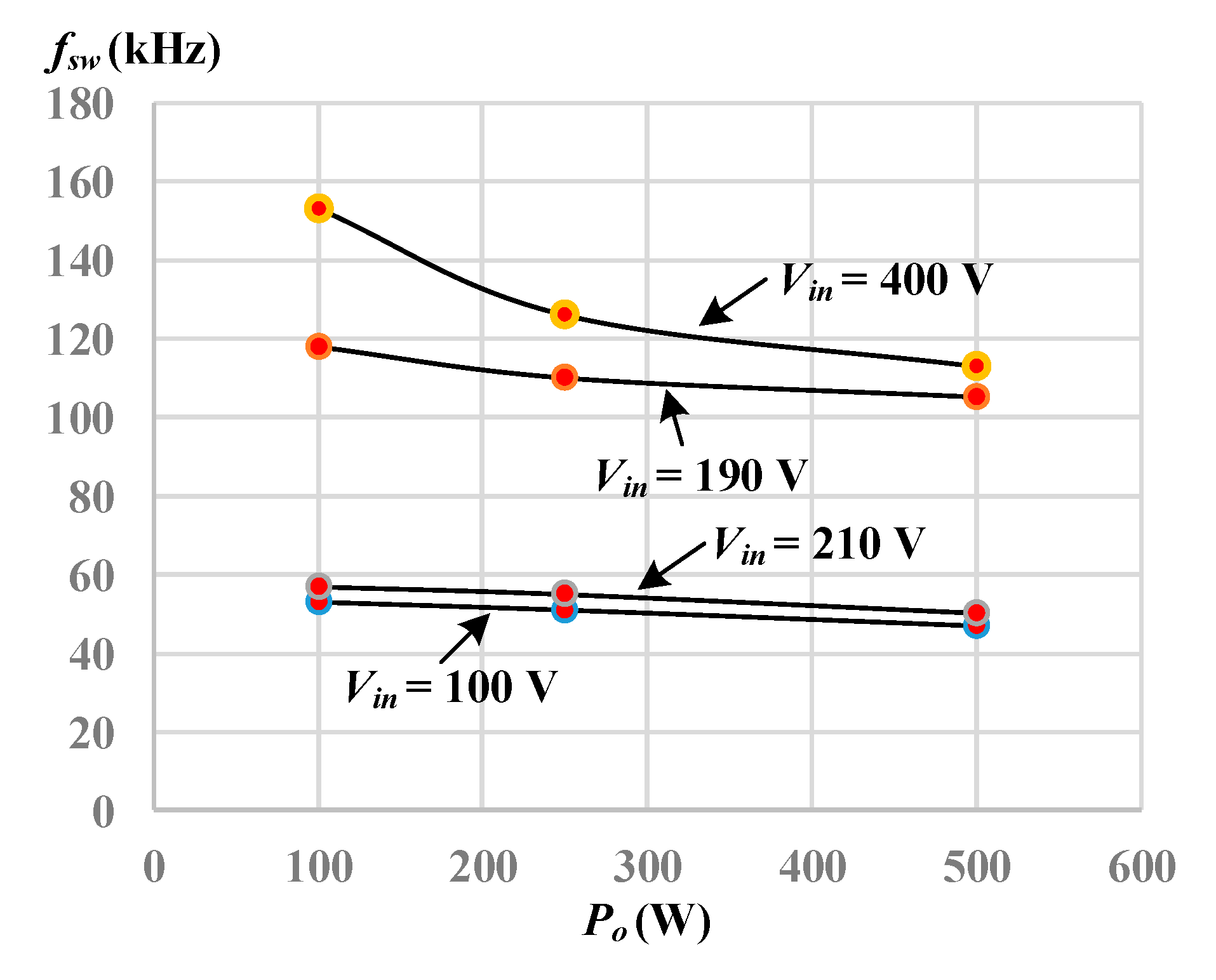
The measured input voltage and the PWM signal of the AC switch Sac are provided in Figure 11. The hysteresis voltage band and reference voltage of the voltage comparator are 10 V and 200 V, respectively. First, the input voltage is increased from 100 V to 400 V. When Vin is greater than 205 V, the PWM signal of Sac is changed from the “on” state (high-voltage) to “off” state (low-voltage). Second, the input voltage is decreased from 400 V. When Vin is less than 195 V, Sac is turned on (high-voltage). Figure 12 gives the experimental switching frequency of the proposed resonant converter. For low-voltage ranges and the same load condition, the voltage gain of the resonant converter under Vin = 100 V is higher than Vin = 190 V. One can see that the measured switching frequency at 100 V input voltage is lower than 190 V input voltage. The experimental circuit efficiencies of the proposed converter at 100% load are 87.3% (100 V input), 91.2% (190 V input), 89.5% (210 V input), and 92.8% (400 V input). Since the turns ratio np/ns is used under high-voltage ranges (Vin = 200–400 V) instead of np/(2ns) under low-voltage ranges (Vin = 100–200 V), the converter has a lower magnetizing current under high-voltage ranges compared to the low-voltage range operation. The converter has lower conduction loss on power switches at high-input voltage ranges. Therefore, the experimental circuit efficiency at 400 V input is better than the 190 V input, and the efficiency with the 210 V input is better than the 100 V input.
5. Conclusions
The half-bridge LLC resonant converter with variable winding turns is studied and implemented in this paper to accomplish two objectives: (1) wide, soft switching ranges over the entire input voltage and output road; and (2) wide voltage operation. The general half-bridge resonant converter is adopted on the high-voltage side to a achieve series resonant circuit and realize the soft switching operation for powered semiconductors. Two sets of winding turns are adopted on the low-voltage side to accomplish wide voltage operation capability. Based on the circuit analysis and test results, the proposed LLC converter can achieve zero voltage switching with wide input voltage (100 V to 400 V) and wide load (20% to 100% rated power) ranges. Compared to the conventional LLC resonant converters with wide voltage operation, the proposed converter has lower component counts, a simple control scheme, and less voltage stress on rectifier diodes. The studied LLC converter can be used for power units in computers and power servers with large hold-up times, PV power converters, fuel cell converters, and battery chargers and dischargers with wide voltage operation. Experimental waveforms from a 500 W prototype are given and presented to confirm the usefulness of the presented circuit topology. The future works will investigate the new wide voltage converters with low cost and high power density advantages for industry power applications and renewable energy power conversion.
Author Contributions
B.-R.L. proposed and designed this project and was responsible for writing the paper. C.-X.D. measured the circuit waveforms in the experiment. All authors have read and agreed to the published version of the manuscript.
Funding
This research is funded by the Ministry of Science and Technology, Taiwan, under grant number MOST 108-2221-E-224-022-MY2.
Acknowledgments
This work is supported by the Ministry of Science and Technology, Taiwan (MOST 108-2221-E-224-022-MY2). In addition, the authors are grateful to the all the editor and the reviewers for their valuable suggestions to improve this paper.
Conflicts of Interest
The author declares no conflict of interest.
References
- Kim, J.Y.; Kim, H.S.; Baek, J.W.; Jeong, D.K. Analysis of effective three-level neutral point clamped converter system for the bipolar LVDC distribution. Electronics 2019, 8, 691. [Google Scholar] [CrossRef] [Green Version]
- Blaabjerg, F.; Dragicevic, T.; Davari, P. Applications of Power Electronics. Electronics 2019, 8, 465. [Google Scholar] [CrossRef] [Green Version]
- Almalaq, Y.; Matin, M. Three topologies of a non-isolated high gian switched-capacitor step-up cuk converter for renewable energy applications. Electronics 2018, 7, 94. [Google Scholar] [CrossRef] [Green Version]
- Tahir, S.; Wang, J.; Balocj, M.H.; Kaloi, G.S. Digital control techniques based on voltage source inverters in renewable energy applications: A review. Electronics 2018, 7, 18. [Google Scholar] [CrossRef] [Green Version]
- Lin, B.R. Phase-shift pwm converter with wide voltage operation capability. Electronics 2020, 9, 47. [Google Scholar] [CrossRef] [Green Version]
- Lin, B.R. Analysis of a dc converter with low primary current loss and balance voltage and current. Electronics 2019, 8, 439. [Google Scholar] [CrossRef] [Green Version]
- Kamal, T.; Karabackk, M.; Hassan, S.Z.; Fernández-Ramírez, L.M.; Riaz, M.H.; Riaz, M.T.; Khan, M.A.; Khan, L. Energy management and switching control of PHEV charging stations in a hybrid smart micro-grid system. Electronics 2018, 7, 156. [Google Scholar] [CrossRef] [Green Version]
- Wang, P.; Zhou, L.; Zhang, Y.; Li, J.; Sumner, M. Input-parallel output-series DC-DC boost converter with a wide input voltage range, for fuel cell vehicles. IEEE Trans. Vehicular Tech. 2017, 66, 7771–7781. [Google Scholar] [CrossRef]
- Lin, B.R.; Hsieh, F.Y. Soft-switching zeta-flyback converter with a buck-boost type of active clamp. IEEE Trans. Ind. Electron. 2007, 54, 2813–2822. [Google Scholar]
- Jeong, Y.; Park, J.D.; Moon, G.W. An interleaved active-clamp forward converter modified for reduced primary conduction loss without additional components. IEEE Trans. Power Electron. 2020, 35, 121–130. [Google Scholar] [CrossRef]
- Lin, B.R.; Chao, C.H. A new ZVS DC/DC converter with three APWM circuits. IEEE Trans. Ind. Electron. 2013, 60, 4351–4358. [Google Scholar] [CrossRef]
- Pont, N.C.D.; Bandeira, D.; Lazzarin, T.B.; Barbi, I. A ZVS APWM half-bridge parallel resonant DC–DC converter with capacitive output. IEEE Trans. Ind. Electron. 2019, 66, 5231–5241. [Google Scholar] [CrossRef]
- Mishima, T.; Akamatsu, K.; Nakaoka, M. A high frequency-link secondary-side phase-shifted full-bridge soft-switching PWM DC-DC converter with ZCS active rectifier for EV battery charger. IEEE Trans. Power Electron. 2013, 28, 5758–5773. [Google Scholar] [CrossRef] [Green Version]
- Pahlevaninezhad, M.; Das, P.; Drobnik, J.; Pain, P.K.; Bakhshai, A. A novel ZVZCS full-bridge DC/DC converter used for electric vehicles. IEEE Trans. Power Electron. 2012, 27, 2752–2769. [Google Scholar] [CrossRef]
- Steigerwald, R.L. A comparison of half-bridge resonant converter topologies. IEEE Trans. Power Electron. 1988, 3, 174–182. [Google Scholar] [CrossRef]
- Lin, B.R.; Chu, C.W. Hybrid full-bridge and LLC converter with wide ZVS range and less output inductance. IET Power Electron. 2016, 9, 377–384. [Google Scholar] [CrossRef]
- Yang, G.; Dubus, P.; Sadarnac, D. Double-phase high-efficiency, wide load range high-voltage/low-voltage LLC DC/DC converter for electric/hybrid vehicles. IEEE Trans. Power Electron. 2015, 30, 1876–1886. [Google Scholar] [CrossRef] [Green Version]
- Lee, J.B.; Kim, J.K.; Baek, J.I.; Kim, J.H.; Moon, G.W. Resonant capacitor on/off control of half-bridge LLC converter for high efficiency server power supply. IEEE Trans. Ind. Electron. 2016, 63, 5410–5415. [Google Scholar] [CrossRef]
- Lu, J.; Kumar, A.; Afridi, K.K. Step-down impedance control network resonant DC-DC converter utilizing an enhanced phase-shift control for wide-input-range operation. IEEE Trans. Ind. Appl. 2018, 54, 4523–4536. [Google Scholar] [CrossRef]
- Hu, H.; Fang, X.; Chen, F.; Shen, Z.J.; Batarseh, I. A modified high-efficiency LLC converter with two transformers for wide input-voltage range applications. IEEE Trans. Power Electron. 2013, 28, 1946–1960. [Google Scholar] [CrossRef]
- Sun, W.; Xing, Y.; Wu, H.; Ding, J. Modified high-efficiency LLC converters with two split resonant branches for wide input-voltage range applications. IEEE Trans. Power Electron. 2018, 33, 7867–7870. [Google Scholar] [CrossRef]
- Jeong, Y.; Kim, J.K.; Lee, J.B.; Moon, G.W. An asymmetric half-bridge resonant converter having a reduced conduction loss for DC/DC power applications with a wide range of low-input voltage. IEEE Trans. Power Electron. 2017, 32, 7795–7804. [Google Scholar] [CrossRef]
- Lin, B.R. Implementation of a Parallel-Series Resonant Converter with Wide Input Voltage Range. Energies 2019, 12, 4095. [Google Scholar] [CrossRef] [Green Version]
- Lin, B.R. Resonant converter with soft switching and wide voltage operation. Energies 2019, 12, 3479. [Google Scholar] [CrossRef] [Green Version]
- Lin, B.R. Resonant converter with wide input voltage range and input current ripple free. IET Proc. Electron. Lett. 2018, 54, 1086–1088. [Google Scholar] [CrossRef]
- Lin, B.R. Series resonant converter with auxiliary winding turns: Analysis, design and implementation. Int. J. Electron. 2018, 105, 836–847. [Google Scholar] [CrossRef]
Figure 1.
Conventional inductor–inductor–capacitor (LLC) converter based on (a) a center-tapped rectifier structure and (b) a voltage double rectifier structure.
Figure 1.
Conventional inductor–inductor–capacitor (LLC) converter based on (a) a center-tapped rectifier structure and (b) a voltage double rectifier structure.

Figure 2.
Circuit structure of (a) the presented converter (b) under low-voltage operation (Sac on) and (c) under high-voltage operation (Sac off).
Figure 2.
Circuit structure of (a) the presented converter (b) under low-voltage operation (Sac on) and (c) under high-voltage operation (Sac off).
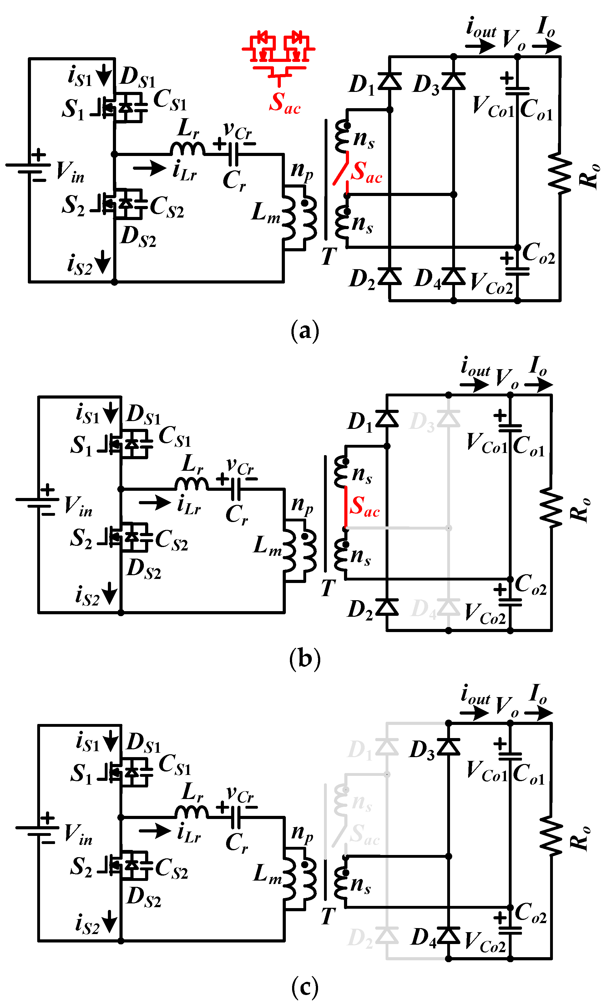
Figure 3.
LLC circuits operated at low-input voltage ranges: (a) pulse width modulation PWM waveforms; (b) mode 1; (c) mode 2; (d) mode 3; (e) mode 4; (f) mode 5; (g) mode 6.
Figure 3.
LLC circuits operated at low-input voltage ranges: (a) pulse width modulation PWM waveforms; (b) mode 1; (c) mode 2; (d) mode 3; (e) mode 4; (f) mode 5; (g) mode 6.


Figure 4.
LLC circuits operated at high-input voltage ranges: (a) PWM waveforms; (b) mode 1; (c) mode 2; (d) mode 3; (e) mode 4; (f) mode 5; (g) mode 6.
Figure 4.
LLC circuits operated at high-input voltage ranges: (a) PWM waveforms; (b) mode 1; (c) mode 2; (d) mode 3; (e) mode 4; (f) mode 5; (g) mode 6.


Figure 5.
Alternating current (AC) equivalent circuit of the resonant tank.

Figure 6.
Circuit diagram of the laboratory prototype.
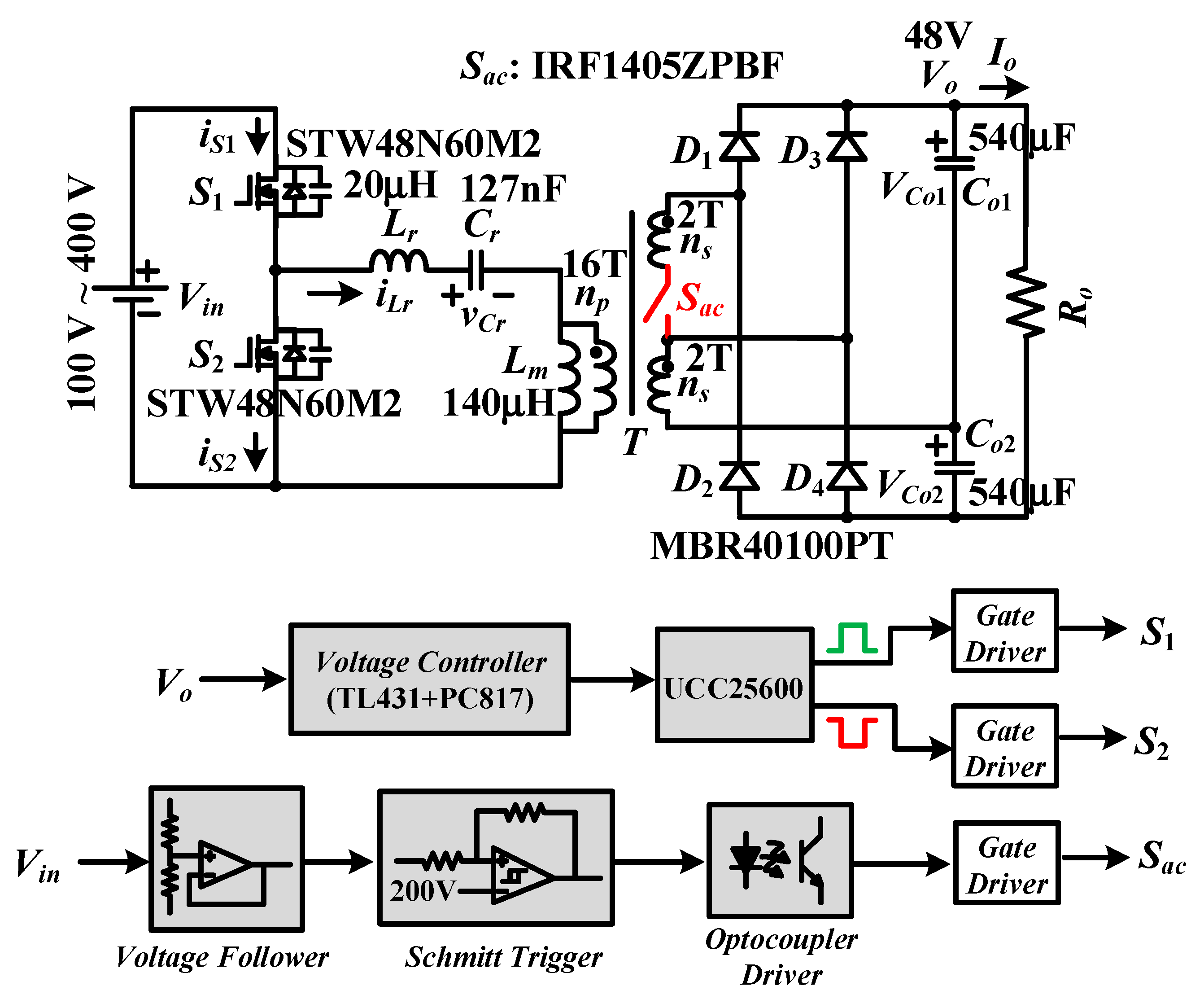
Figure 7.
Measured results of vS1,g, vS2,g, vCr, and iLr at rated power values of:(a) Vin = 100 V; (b) Vin = 190 V; (c) Vin = 210 V; (d) Vin = 400 V.
Figure 7.
Measured results of vS1,g, vS2,g, vCr, and iLr at rated power values of:(a) Vin = 100 V; (b) Vin = 190 V; (c) Vin = 210 V; (d) Vin = 400 V.

Figure 8.
Measured results of the secondary side diode currents at rated power values of: (a) Vin = 100 V; (b) Vin = 190 V; (c) Vin = 210 V; (d) Vin = 400 V.
Figure 8.
Measured results of the secondary side diode currents at rated power values of: (a) Vin = 100 V; (b) Vin = 190 V; (c) Vin = 210 V; (d) Vin = 400 V.

Figure 9.
Measured results of vS1,g, vS1,d, and iS1 at 20% power; (a) Vin = 100 V; (b) Vin = 190 V; (c) Vin = 210 V; (d) Vin = 400 V.
Figure 9.
Measured results of vS1,g, vS1,d, and iS1 at 20% power; (a) Vin = 100 V; (b) Vin = 190 V; (c) Vin = 210 V; (d) Vin = 400 V.

Figure 10.
Measured results of vS1,g, vS1,d, and iS1 at the rated power values of: (a) Vin = 100 V; (b) Vin = 190 V; (c) Vin = 210 V; (d) Vin = 400 V.
Figure 10.
Measured results of vS1,g, vS1,d, and iS1 at the rated power values of: (a) Vin = 100 V; (b) Vin = 190 V; (c) Vin = 210 V; (d) Vin = 400 V.

Figure 11.
The experimental waveforms of the input voltage Vin and PWM signal of Sac.
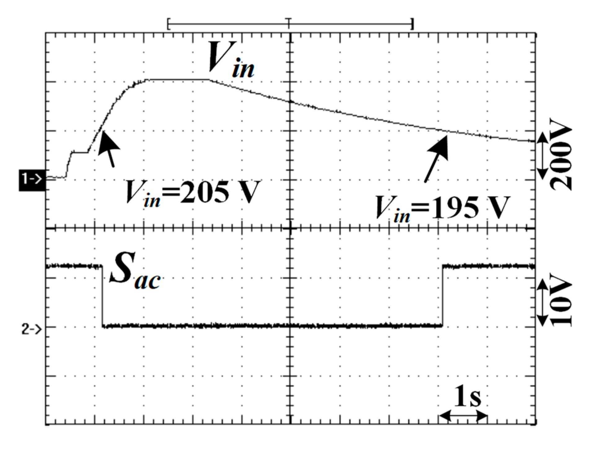
Figure 12.
Measured switching frequency under various input voltages and load conditions.
© 2020 by the authors. Licensee MDPI, Basel, Switzerland. This article is an open access article distributed under the terms and conditions of the Creative Commons Attribution (CC BY) license (http://creativecommons.org/licenses/by/4.0/).
Share and Cite
MDPI and ACS Style
Lin, B.-R.; Dai, C.-X. Wide Voltage Resonant Converter Using a Variable Winding Turns Ratio. Electronics 2020, 9, 370. https://doi.org/10.3390/electronics9020370
AMA Style
Lin B-R, Dai C-X. Wide Voltage Resonant Converter Using a Variable Winding Turns Ratio. Electronics. 2020; 9(2):370. https://doi.org/10.3390/electronics9020370
Chicago/Turabian StyleLin, Bor-Ren, and Chu-Xian Dai. 2020. "Wide Voltage Resonant Converter Using a Variable Winding Turns Ratio" Electronics 9, no. 2: 370. https://doi.org/10.3390/electronics9020370
Note that from the first issue of 2016, this journal uses article numbers instead of page numbers. See further details here.