Design and Implementation of 150 W AC/DC LED Driver with Unity Power Factor, Low THD, and Dimming Capability

 ,
,
Abstract
:
1. Introduction
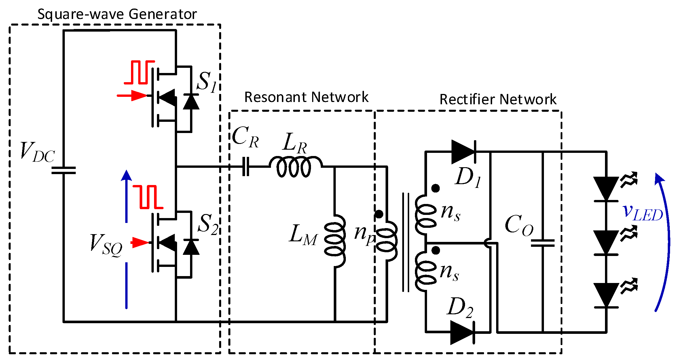
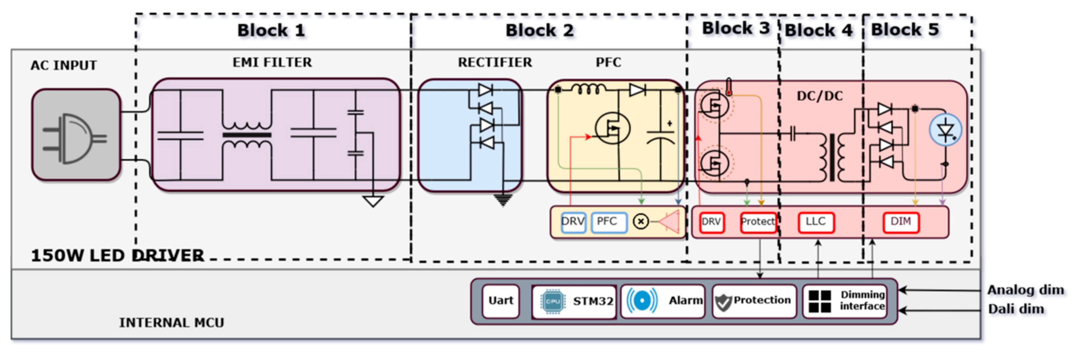
2. Principle Operation of Two-Stage LED Driver
2.1. Principle Operation of Boost PFC Converter
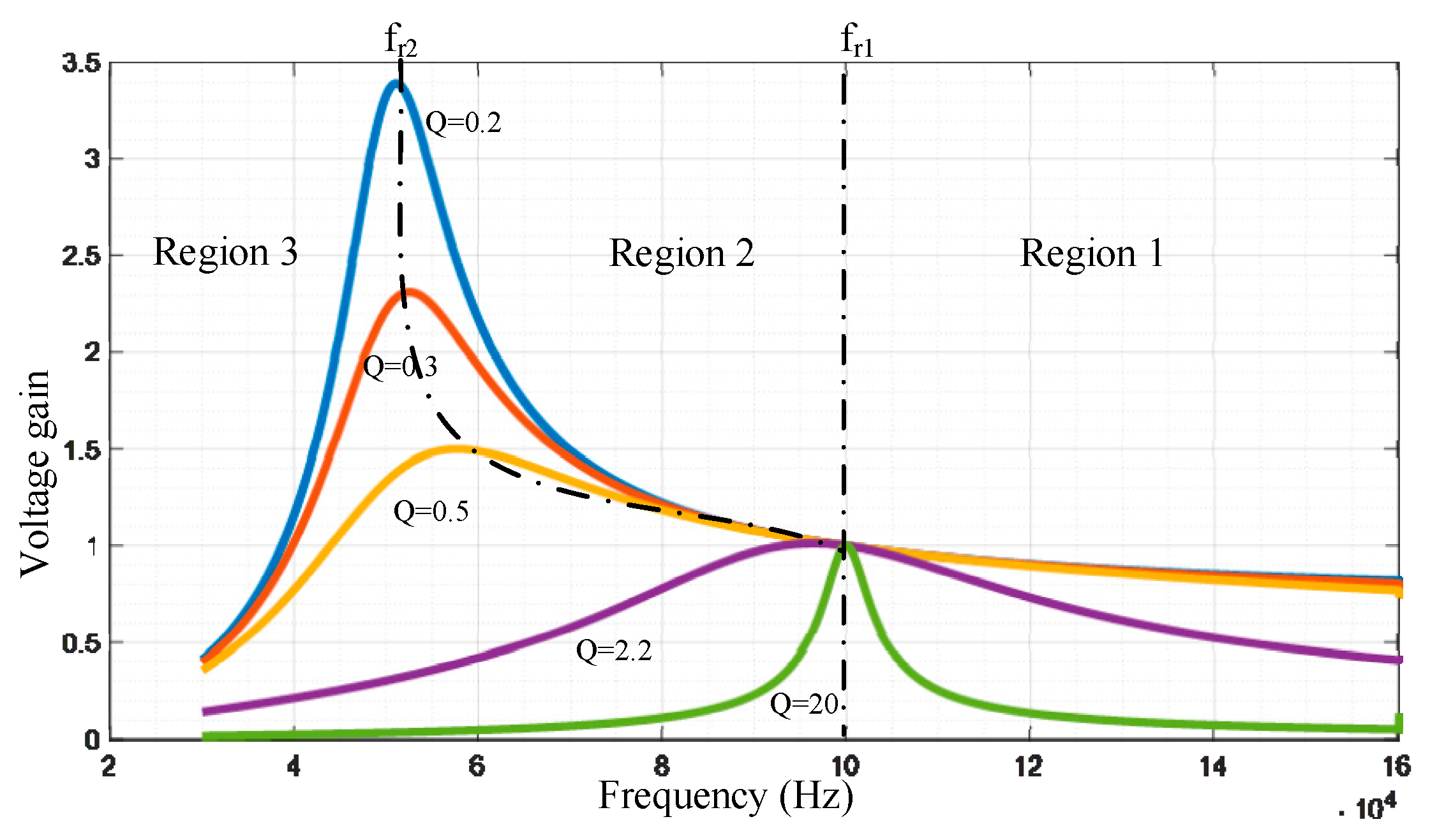
2.2. Principle Operation of LLC Resonant Converter
3. Design Procedure of the Two-Stage LED Driver
3.1. Boost-PFC Stage Design
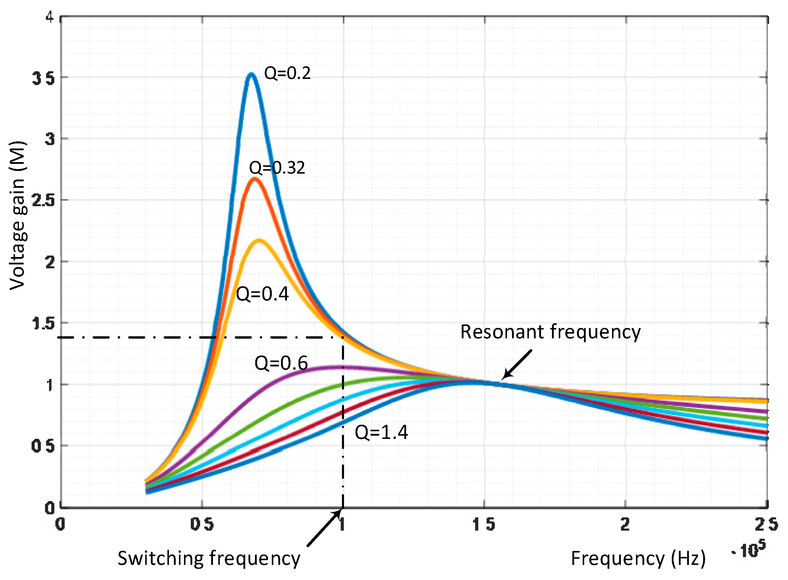
3.2. LLC Resonant DC-DC Converter Design
3.3. EMI Design
3.4. Dimming Control
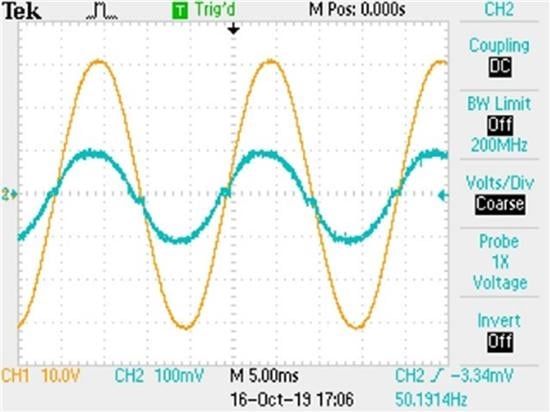
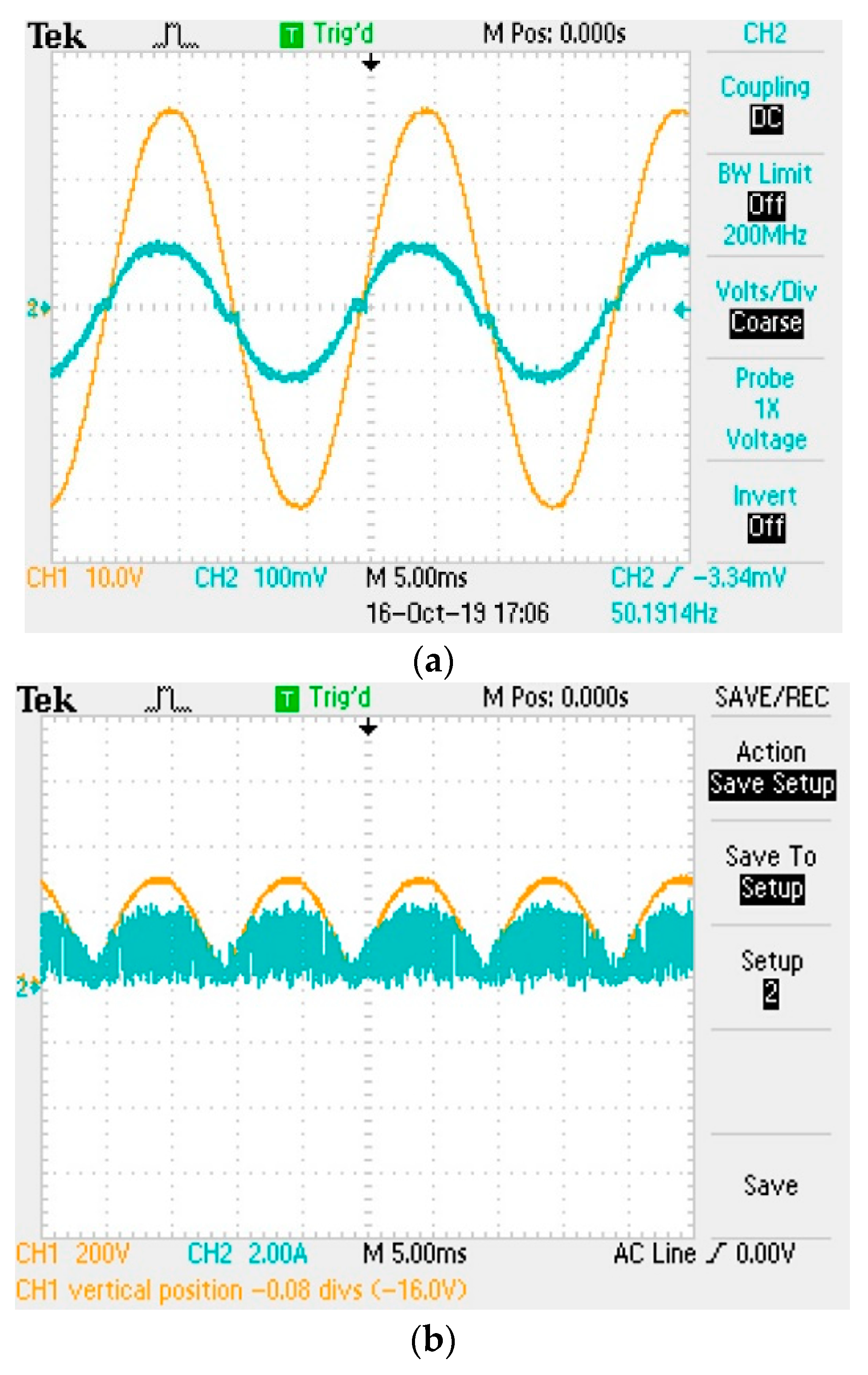
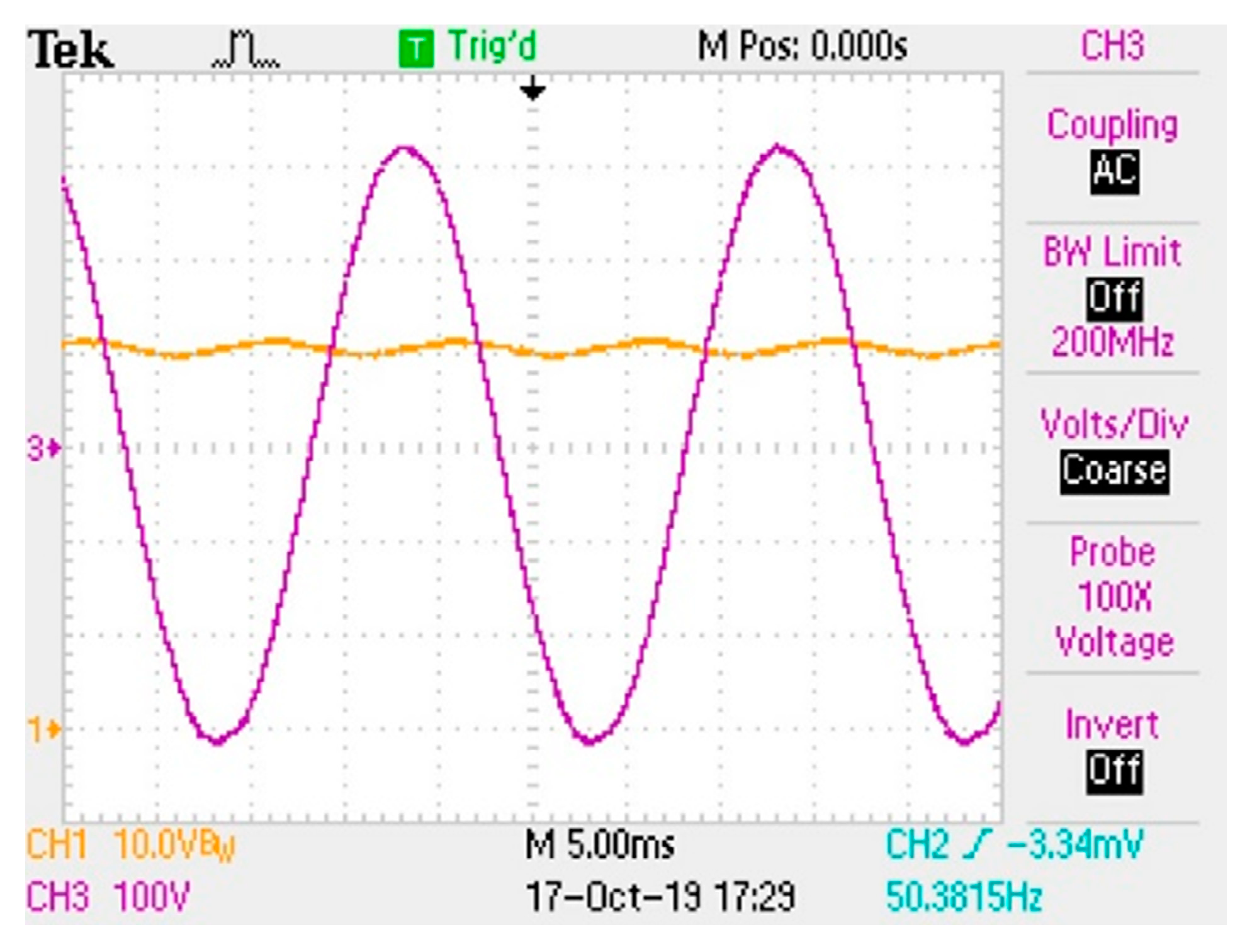
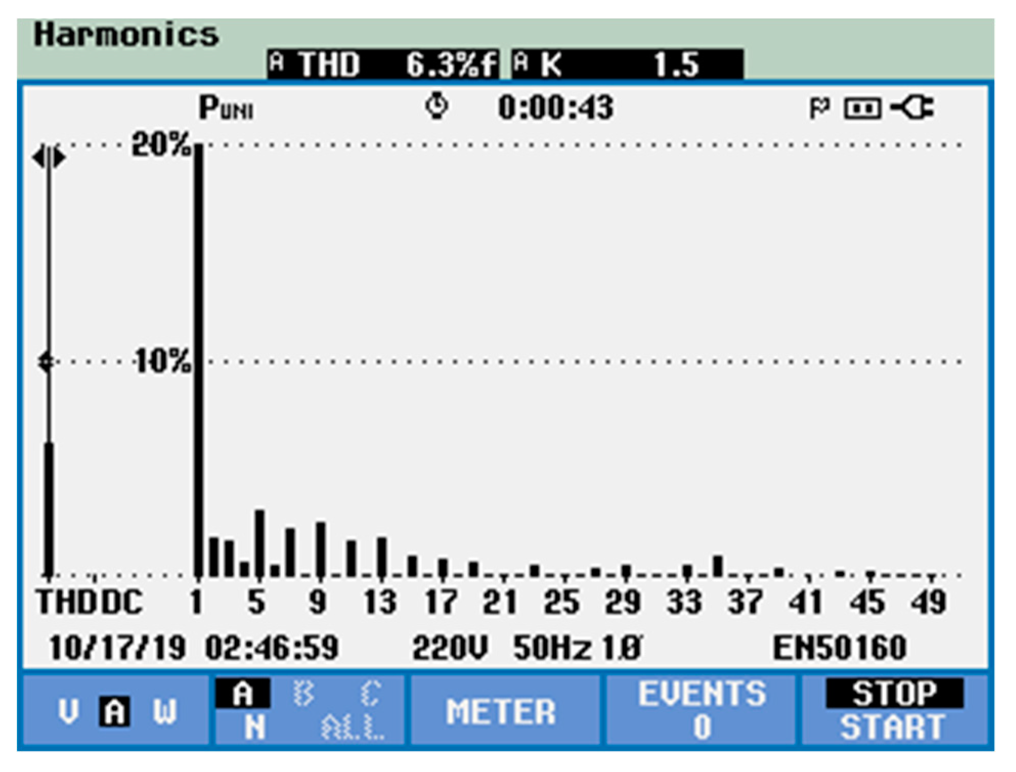
4. Hardware Prototype and Experimental Results
5. Conclusions
Author Contributions
Funding
Conflicts of Interest
References
- Uddin, S.; Shareef, H.; Mohamed, A.; Hannan, M.A.; Mohamed, K. LEDs as energy efficient lighting systems: A detail review. In Proceedings of the 2011 IEEE Student Conference on Research and Development, Cyberjaya, Malaysia, 19–20 December 2011; pp. 468–472. [Google Scholar]
- Jin, H.; Jin, S.; Chen, L.; Cen, S.; Yuan, K. Research on the Lighting Performance of LED Street Lights with Different Color Temperatures. IEEE Photonics J. 2015, 7, 1–9. [Google Scholar] [CrossRef]
- Wu, C.-Y.; Wu, T.-F.; Tsai, J.-R.; Chen, Y.-M.; Chen, C.-C. Multistring LED Backlight Driving System for LCD Panels with Color Sequential Display and Area Control. IEEE Trans. Ind. Electron. 2008, 55, 3791–3800. [Google Scholar]
- Wang, Y.; Alonso, J.M.; Ruan, X. A Review of LED Drivers and Related Technologies. IEEE Trans. Ind. Electron. 2017, 64, 5754–5765. [Google Scholar] [CrossRef]
- Cheng, C.-A.; Cheng, H.-L.; Chung, T.-Y. A Novel Single-Stage High-Power-Factor LED Street-Lighting Driver with Coupled Inductors. IEEE Trans. Ind. Appl. 2014, 50, 3037–3045. [Google Scholar] [CrossRef]
- Mangkalajan, S.; Ekkaravarodome, C.; Jirasereeamornkul, K.; Thounthong, P.; Higuchi, K.; Kazimierczuk, M.K. A Single-Stage LED Driver Based on ZCDS Class-E Current-Driven Rectifier as a PFC for Street-Lighting Applications. IEEE Trans. Power Electron. 2018, 33, 8710–8727. [Google Scholar] [CrossRef]
- Cheng, C.-A.; Chang, C.-H.; Chung, T.-Y.; Yang, F.-L. Design and Implementation of a Single-Stage Driver for Supplying an LED Street-Lighting Module with Power Factor Corrections. IEEE Trans. Power Electron. 2015, 30, 956–966. [Google Scholar] [CrossRef]
- Camponogara, D.; Ferreira, G.F.; Campos, A.; Costa, M.A.D.; Garcia, J. Offline LED Driver for Street Lighting with an Optimized Cascade Structure. IEEE Trans. Ind. Appl. 2013, 49, 2437–2443. [Google Scholar] [CrossRef]
- Lee, E.S.; Choi, B.H.; Nguyen, D.T.; Choi, B.G.; Rim, C.T. Static Regulated Multistage Semiactive LED Drivers for High-Efficiency Applications. IEEE Trans. Power Electron. 2015, 31, 6543–6552. [Google Scholar] [CrossRef]
- Lin, W.; Chen, H.; Ke, S. Research on a single-stage Flyback/boost LED driver with lower output ripple. In Proceedings of the 2016 IEEE 2nd Annual Southern Power Electronics Conference (SPEC), Auckland, New Zealand, 5–8 December 2016; pp. 1–5. [Google Scholar]
- Guo, Y.; Li, S.; Lee, A.T.L.; Tan, S.-C.; Lee, C.K.; Hui, S.Y.R. Single-Stage AC/DC Single-Inductor Multiple-Output LED Drivers. IEEE Trans. Power Electron. 2015, 31, 5837–5850. [Google Scholar] [CrossRef]
- Wang, Y.; Guan, Y.; Xu, D.; Wang, W. A CLCL Resonant DC/DC Converter for Two-Stage LED Driver System. IEEE Trans. Ind. Electron. 2015, 63, 2883–2891. [Google Scholar] [CrossRef]
- Athalye, P.; Harris, M.; Negley, G. A two-stage LED driver for high-performance high-voltage LED fixtures. In Proceedings of the 2012 Twenty-Seventh Annual IEEE Applied Power Electronics Conference and Exposition (APEC), Orlando, FL, USA, 5–9 February 2012; pp. 2385–2391. [Google Scholar]
- Xie, X.; Ye, M.; Cai, Y.; Wu, J. An optocouplerless two-stage high power factor LED driver. In Proceedings of the 2011 Twenty-Sixth Annual IEEE Applied Power Electronics Conference and Exposition (APEC), Fort Worth, TX, USA, 6–11 March 2011; pp. 2078–2083. [Google Scholar]
- Lin, W.; Yuzhen, X.; Zheng, Q.L. A high efficiency integrated step-down Cuk and flyback converter for LED power driver. In Proceedings of the 2015 9th International Conference on Power Electronics and ECCE Asia (ICPE-ECCE Asia), Seoul, Korea, 1–5 June 2015; pp. 60–64. [Google Scholar]
- Lee, S.-W.; Do, H.-L. Boost-Integrated Two-Switch Forward AC–DC LED Driver with High Power Factor and Ripple-Free Output Inductor Current. IEEE Trans. Ind. Electron. 2017, 64, 5789–5796. [Google Scholar] [CrossRef]
- Wang, Y.; Deng, X.; Wang, Y.; Xu, D. Single-Stage Bridgeless LED Driver Based on a CLCL Resonant Converter. IEEE Trans. Ind. Appl. 2018, 54, 1832–1841. [Google Scholar] [CrossRef]
- Zuo, L.; Qin, H.; Ma, L.; Fang, T. Design and implementation of LLC Half-bridge LED driver based on NCP1396. In Proceedings of the 2011 International Conference on Electrical and Control Engineering, Yichang, China, 16–18 September 2011; pp. 4424–4426. [Google Scholar]
- Zawawi, N.A.; Iqbal, S.; Jamil, M.K.M. Implementation of a single-stage LED driver using resonant controller. In Proceedings of the 2016 6th International Conference on Intelligent and Advanced Systems (ICIAS), Kuala Lumpur, Malaysia, 15–17 August 2016; pp. 1–6. [Google Scholar]
- Deng, C.; Chen, M.; Chen, P.; Hu, C.; Zhang, W.; Xu, D. A PFC Converter with Novel Integration of Both the EMI Filter and Boost Inductor. IEEE Trans. Power Electron. 2014, 29, 4485–4489. [Google Scholar] [CrossRef]
- Majid, A.; Saleem, J.; Kotte, H.B.; Ambatipudi, R.; Bertilsson, K. Design and implementation of EMI filter for high frequency (MHz) power converters. In Proceedings of the International Symposium on Electromagnetic Compatibility—EMC EUROPE, Rome, Italy, 17–21 September 2012; pp. 1–4. [Google Scholar]
- Fan, J.W.; Chow, J.P.-W.; Chan, W.-T.; Zhang, K.; Relekar, A.; Ho, K.-W.; Tung, C.-P.; Wang, K.-W.; Chung, H.S.-H. Modeling and Experimental Assessment of the EMI Characteristics of Switching Converters with Power Semiconductor Filters. IEEE Trans. Power Electron. 2020, 35, 2519–2533. [Google Scholar] [CrossRef]
- King, R.; Stuart, T. A Normalized Model for the Half-Bridge Series Resonant Converter. IEEE Trans. Aerosp. Electron. Syst. 1981, 17, 190–198. [Google Scholar] [CrossRef]
- Shrivastava, A.; Singh, B. LLC series resonant converter-based LED lamp driver with ZVS. In Proceedings of the 2012 IEEE Fifth Power India Conference, Murthal, India, 19–22 December 2012; pp. 1–5. [Google Scholar]
- Ma, J.; Wei, X.; Hu, L.; Zhang, J. LED Driver Based on Boost Circuit and LLC Converter. IEEE Access 2018, 6, 49588–49600. [Google Scholar] [CrossRef]
- Wang, Y.; Guan, Y.; Ren, K.; Wang, W.; Xu, D.; Yueshi, G. A Single-Stage LED Driver Based on BCM Boost Circuit and LLC Converter for Street Lighting System. IEEE Trans. Ind. Electron. 2015, 62, 5446–5457. [Google Scholar] [CrossRef]
- Cheng, C.-A.; Chang, C.-H.; Cheng, H.-L.; Chang, E.-C.; Chung, T.-Y.; Chang, M.-T. A Single-Stage LED Streetlight Driver with Soft-Switching and Interleaved PFC Features. Electronics 2019, 8, 911. [Google Scholar] [CrossRef] [Green Version]
- Available online: https://www.onsemi.com/pub/Collateral/NCP1608-D.PDF (accessed on 18 December 2019).
- Available online: https://www.onsemi.com/products/power-management/led-drivers/ac-dc-led-drivers/fls2100xs (accessed on 18 December 2019).
- Available online: https://katalog.we-online.de/pbs/datasheet/760895441.pdf (accessed on 18 December 2019).
- Nassary, M.; Orabi, M.; Arias, M.; Ahmed, E.M.; Hasaneen, E.-S. Analysis and Control of Electrolytic Capacitor-Less LED Driver Based on Harmonic Injection Technique. Energies 2018, 11, 3030. [Google Scholar] [CrossRef] [Green Version]
- Zhai, L.; Zhang, T.; Cao, Y.; Yang, S.; Kavuma, S.; Feng, H. Conducted EMI Prediction and Mitigation Strategy Based on Transfer Function for a High-Low Voltage DC-DC Converter in Electric Vehicle. Energies 2018, 11, 1028. [Google Scholar] [CrossRef] [Green Version]


| Boost PFC Design Parameters | ||
|---|---|---|
| Input voltage | 220 V | Vin |
| Frequency | 50 Hz | fin |
| Output voltage | 400 V | VDC |
| Input power | 150 W | P |
| Minimum Efficiency | 92% | ηmin |
| Minimum switching frequency | 40 kHz | fsw(min) |
| Boost PFC Design Specification | |
|---|---|
| Diode Rectifier (DR1, DR2, DR3, DR4) | TS15P05GC2 (Taiwan Semiconductor) |
| Boost Inductor LB | 300 µ (Core PQ2625) |
| Mosfet SPFC | STF13NM60N (STMicroelectronics) |
| Boost Diode DB | STTH15R06FP (STMicroelectronics) |
| Cbulk | 100µF/450V (Nichion) |
| IC | NCP1608BDR2G (Onsemi) |
| LLC Resonant Half-Bridge Design Parameters | ||
|---|---|---|
| Half-bridge input voltage | 390–410 V | VDC |
| Switching frequency | 100–120 kHz | fsw |
| Output voltage | 32 V | VLED |
| Output current | 4.7 A | ILED |
| LLC Resonant Half-Bridge Design Parameters | |
|---|---|
| Transformer | ETD 34 (35:4:4) |
| Switching frequency | 100–120 kHz |
| Resonant Inductor LR | 100 µH |
| Magnetizing Inductor LM | 500 µH |
| Resonant Capacitor | 10 nF |
| Didoe D1, D2 | STPS30H60CFP |
| Mosfet S1, S2 and Driver | IC FLS2100XS |
| Feedback Isolation Optocoupler | PC817 |
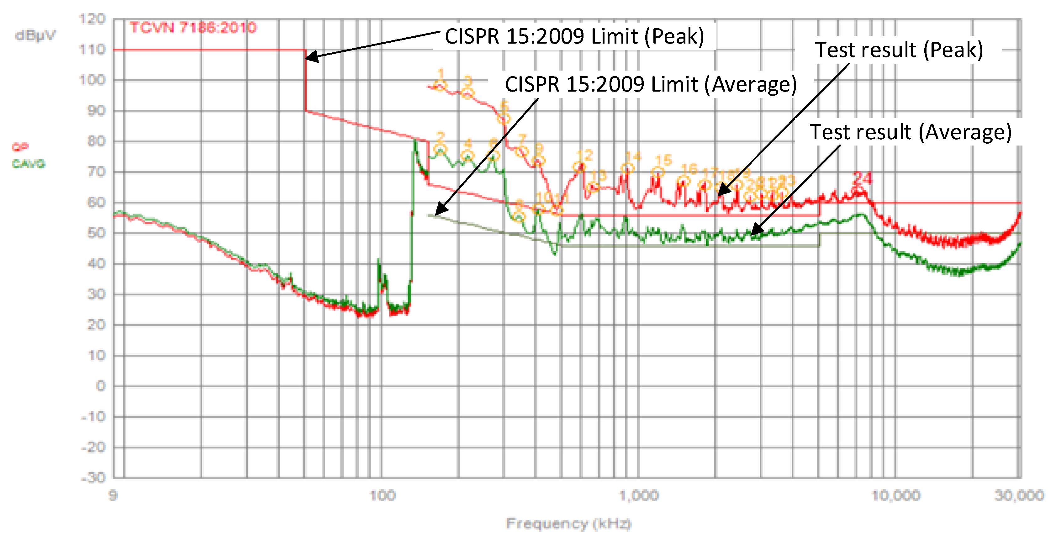
| ID | Frequency | Average Value (dBµV) | Peak Value (dBµV) | Standard CISPR 15:2009 (dBµV) | Distinguished Limit (dBµV) |
|---|---|---|---|---|---|
| 1 | 168 kHz | 68.3 | 98.3 | 65.1 | 33.2 |
| 3 | 213 kHz | 65.8 | 95.8 | 63.1 | 32.7 |
| 5 | 294 kHz | 57.5 | 87.5 | 60.4 | 27.1 |
| 7 | 348 kHz | 46.8 | 76.8 | 59.0 | 17.8 |
| 9 | 402 kHz | 43.7 | 73.7 | 57.8 | 15.8 |
| 12 | 582 kHz | 41.6 | 71.6 | 56.0 | 15.6 |
| 14 | 888 kHz | 41.1 | 71.1 | 56.0 | 15.1 |
| 15 | 1176 kHz | 39.8 | 69.8 | 56.0 | 13.8 |
| 16 | 1473 kHz | 37.0 | 67.0 | 56.0 | 11.0 |
| 17 | 1779 kHz | 35.8 | 65.8 | 56.0 | 9.8 |
| 19 | 2373 kHz | 35.7 | 65.7 | 56.0 | 9.7 |
| Component | Values |
|---|---|
| Cy1, Cy2 | 1 nF/400 V |
| Cy-f1, Cy-f2, Cy-f3 | 1 nF/400 V |
| Cx1, Cx2 | 470 nF/240 V |
| LCM | 40 mH |
| LDM | 170 µH |
| Lcom | 20 mH |
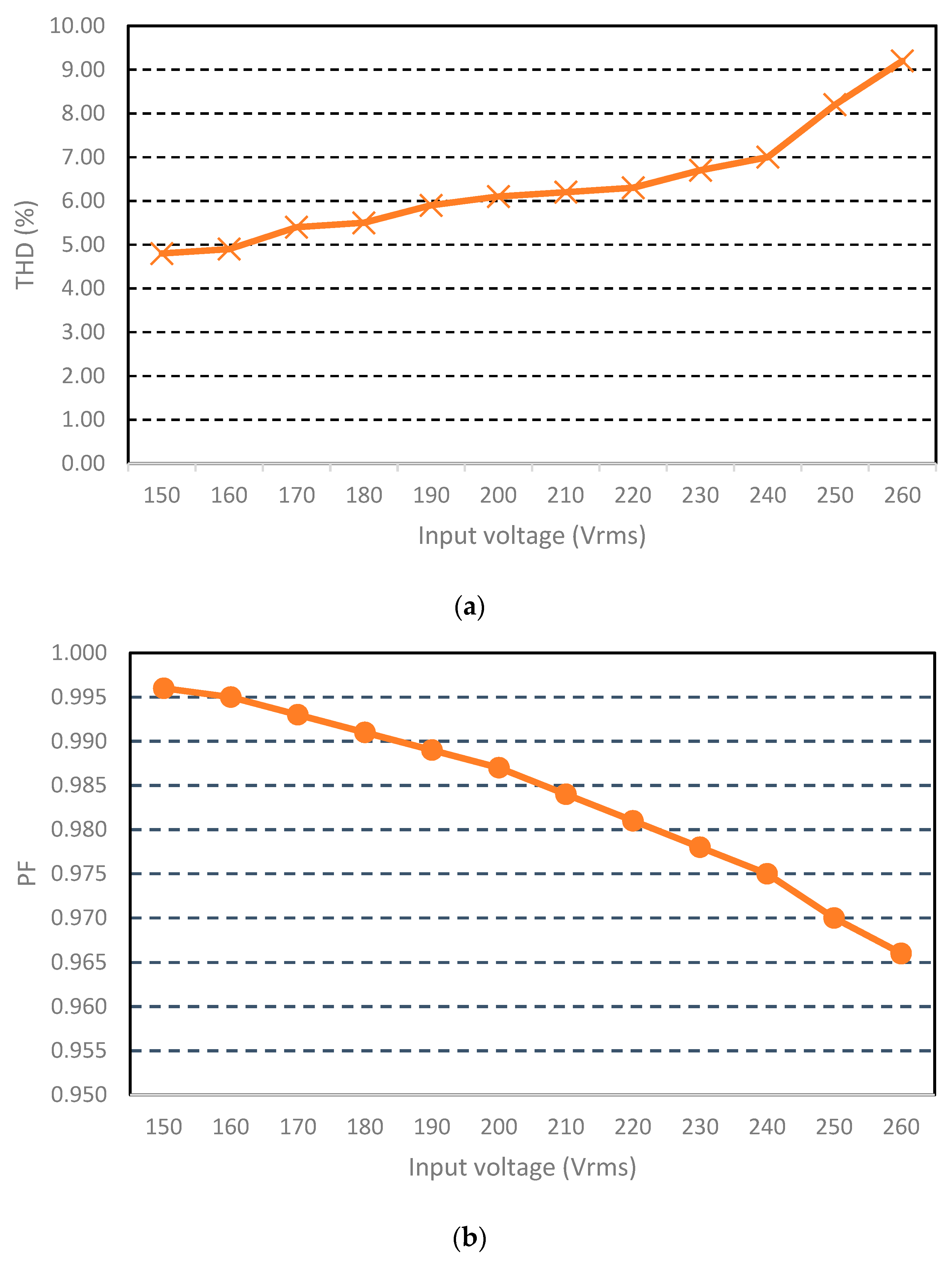
| Input Voltage (V) | Input Current (A) | Input Power (W) | Output Voltage (V) | Output Current (A) | Output Power | Efficiency % | Power Factor | THD % |
|---|---|---|---|---|---|---|---|---|
| 260.7 | 0.676 | 170.1 | 31.33 | 4.995 | 156.5 | 92.00 | 0.966 | 9.20% |
| 250.3 | 0.7 | 169.8 | 31.33 | 4.98 | 156.0 | 91.89 | 0.97 | 8.20% |
| 240.4 | 0.731 | 171.1 | 31.38 | 5.003 | 157.0 | 91.76 | 0.975 | 7.10% |
| 230.9 | 0.76 | 171.5 | 31.41 | 4.993 | 156.8 | 91.45 | 0.978 | 6.70% |
| 220.8 | 0.786 | 170.3 | 31.32 | 4.985 | 156.1 | 91.68 | 0.981 | 6.40% |
| 210.2 | 0.824 | 170.4 | 31.32 | 4.987 | 156.2 | 91.66 | 0.984 | 6.20% |
| 200.3 | 0.866 | 171.1 | 31.33 | 5.003 | 156.7 | 91.61 | 0.987 | 6.10% |
| 190.2 | 0.907 | 170.6 | 31.32 | 4.987 | 156.2 | 91.56 | 0.989 | 5.90% |
| 180.6 | 0.955 | 171 | 31.31 | 4.995 | 156.4 | 91.46 | 0.991 | 5.50% |
| 170.2 | 1.012 | 171.1 | 31.31 | 4.994 | 156.4 | 91.39 | 0.993 | 5.40% |
| 160.2 | 1.075 | 171.2 | 31.3 | 4.988 | 156.1 | 91.19 | 0.995 | 4.90% |
| 150.5 | 1.144 | 171.4 | 31.3 | 4.985 | 156.0 | 91.03 | 0.996 | 4.80% |
© 2019 by the authors. Licensee MDPI, Basel, Switzerland. This article is an open access article distributed under the terms and conditions of the Creative Commons Attribution (CC BY) license (http://creativecommons.org/licenses/by/4.0/).
Share and Cite
Tung, N.T.; Tuyen, N.D.; Huy, N.M.; Phong, N.H.; Cuong, N.C.; Phuong, L.M. Design and Implementation of 150 W AC/DC LED Driver with Unity Power Factor, Low THD, and Dimming Capability. Electronics 2020, 9, 52. https://doi.org/10.3390/electronics9010052
Tung NT, Tuyen ND, Huy NM, Phong NH, Cuong NC, Phuong LM. Design and Implementation of 150 W AC/DC LED Driver with Unity Power Factor, Low THD, and Dimming Capability. Electronics. 2020; 9(1):52. https://doi.org/10.3390/electronics9010052
Chicago/Turabian StyleTung, Ngo Thanh, Nguyen Dinh Tuyen, Nguyen Minh Huy, Nguyen Hoai Phong, Ngo Cao Cuong, and Le Minh Phuong. 2020. "Design and Implementation of 150 W AC/DC LED Driver with Unity Power Factor, Low THD, and Dimming Capability" Electronics 9, no. 1: 52. https://doi.org/10.3390/electronics9010052