Polarization-Independent Tunable Ultra-Wideband Meta-Absorber in Terahertz Regime


Beijing Key Laboratory of Network System Architecture and Convergence, Beijing University of Posts and Telecommunications, Beijing 100876, China
*
Author to whom correspondence should be addressed.
Electronics 2019, 8(8), 831; https://doi.org/10.3390/electronics8080831
Submission received: 23 May 2019
/
Revised: 16 July 2019
/
Accepted: 17 July 2019
/
Published: 26 July 2019
(This article belongs to the Special Issue Applications of Electromagnetic Waves)
Abstract
:In this paper, we demonstrate an ultra-broadband terahertz bilayer graphene-based absorption structure. It has two stacking graphene layers sandwiched by an Au cylinders array, backed by a metallic ground plane. Au cylinders are used to adjust the input impedance to be closely matched to the free space, enabling an ultra-broadband absorption. The absorption spectrum of the bilayer graphene-based absorption structure with Au cylinder arrays shows a bandwidth of 7.1 THz, with the absorption exceeding 80%. The achieved ultra-wideband THz meta-absorber has high absorption, independence of polarization property, simultaneously, illustrating to be a promising candidate for teraherz broadband absorption application.
1. Introduction
The terahertz (THz) range of the electromagnetic spectrum, located between microwave and infrared band, has received fast growing research interest in the past two decades, due to extensive applications such as safety inspection, imaging, sensing, material detection, secure communication and so on in virtue of its unique properties [1,2,3,4,5]. The THz absorbing structure has been part of important elements in these THz applications. Limited by the lack of natural absorbing materials in the terahertz gap, metamaterial absorbers (MAs), where the periodic elements are much smaller than the working wavelength of THz waves, have been considered to be an effective solution [6,7,8,9,10]. Therefore, the emergence of terahertz metamaterials brings new opportunities for the development and application of terahertz absorbing technology. MAs are generally realized by using lossy materials in periodic patterns. According to the equivalent medium theory, by reducing transmission and reflection, the energy of the electromagnetic wave is confined in the material, thus illustrating absorption characteristics.
However, THz MAs studied to date still exhibit compromised performance between broadband operation, high absorption, polarization dependence, angle insensitivity and structural complexity. Long Ju and Yongzhi Cheng proposed the polarization independent tunable absorber, however, the mechanism of metamaterial resonance absorption still makes the absorption bandwidth of metamaterials narrow and limit the practical application [11,12]. Yannan Jiang et al. studied a wide-angle incidence Tunable Terahertz Absorber, but the tunable range is only about 1 THz [13]. In addition, dual-band, multi-band and broadband terahertz metamaterial absorber has attracted more attention from engineering researchers [14,15,16,17]. To achieve broadband absorption, one way is tantamount to merge multiple resonators in one cell [18,19,20,21]. Another strategy is used by stacking structure or cascading the multi-layered sheet with different frequency responses separated by dielectric with different thicknesses [22,23,24]. Delin Jia designed a broadband THz bi-metasurfaces absorber composed of two stacking metasurfaces [25]. The absorber combines the above two methods by horizontally arranging multiplexed resonators on each planar layer and then vertically stacking the two layers. However, the absorption rate is lower than 60% at the middle part of the spectrum, and lack of the wide-angle incidence characteristics.
Motivated by the methods and structures of researches to achieve broad angle [26,27], and high absorption [28,29], and driven by the essential need for polarization-independent ultra-wideband meta-absorber, we theoretically investigate a bilayer graphene-based absorption structure with Au cylinder arrays on parylene substrate. We use the cascading bilayer graphene structure with two different frequency resonances. The first graphene layer achieves wave absorption in low frequency band, the second graphene layer achieves wave absorption in high frequency band. Due to the two frequency bands are close to each other, we put the two graphene layers together with cascading structure. To achieve as high absorption as possible, we need to have the input impedance of the whole structure to be as close to the impedance of free space. However, the cascading structure suffers an unsatisfactory impedance matching, then the metallic cylinders are attached to improve the impedance matching of the whole structure. Finally, we have the ultra-broadband Meta-absorber about 7.1 THz with absorption higher than 80% with polarization insensitive for both TE and TM polarizations.
2. Models and Design
The schematic of the proposed absorption structure is depicted in Figure 1. The whole structure consists of cylinders array with the first graphene on the top, and substrate with second graphene on the top and the metallic layer on the bottom. Both the first graphene layer and the second graphene layer use the gradient diameter of the graphene sheet as the resonance unit cell. Aiming to obtain absorption peaks at low frequency, the period of the top graphene is 75 m, employing one outer annulus with outer radius m, inner annulus with outer radius m, and inner circle disk with radius m. The gap between outer annulus with inner annulus and inner annulus with inner circle disk are m and m, respectively. To get an absorption targeting at high spectrum, the second graphene has an 18.75 m periodicity of resonators array with a 25% fill factor, thus making the bilayer graphene-based absorber has a periodicity P of 75 m. The bottom graphene layer consists of 16 identical circle disks, each one has one outer annulus with outer radius m, and inner annulus with outer radius m, and inner circle disk with radius m. The gap between outer annulus with inner annulus and inner annulus with inner circle disk are m and m, respectively. As shown in Figure 1, four Au cylinders as resonators are periodically arranged in both the x- and y-directions. The radius of the Au cylinder, and the height of the Au cylinder are denoted as m and m, respectively. At the bottom layer, Au is also selected as the ground plate, whose conductivity is described by Drude model as , with , s and s [30]. The low loss parylene with thickness m is chosen as the substrate. A permittivity and loss are used to model the parylene film. The electrical vector of plane wave is parallel to x-direction in simulation. The bilayer graphene can be modeled as a 2-D surface, with surface conductivity of top layer for top graphene layer and for second graphene layer. In the terahertz range, for both and , governed by the Kubo formula including the interband and intraband transition contributions [11]. The contribution of the interband is negligible compared with the intraband , which can be expressed as:
where is the Boltzmann’s constant, T is the temperature in Kelvin, e is the electron charge, and , is the chemical potential. Moreover, , are the angular frequency, ℏ is the reduced Planck’s constant, , is the electron relaxation time, and , are the electron scattering rate. Here assuming K and , . The whole structure, including the bilayer graphene and four Au cylinder arrays, is objected to possess the symmetry principle, ensuring the insensitivity to the polarization of electromagnetic waves. The dimensions of the whole structure are optimized with HFSS software. The absorption rate is described as , where , , and represent frequency dependent absorptivity, reflectivity, and transmission rate, respectively. Moreover, the transmissivity of the structure is equal to 0 due to the gold-backed slab (), leading to the absorption rate .
3. Simulation and Results
In the simulation, the first graphene layer is set as impedance boundary1 with resistance1: , and reactance1: . In addition, the second graphene layer is set as impedance boundary2 with resistance2: , and reactance2: . Where, , .
Master-Slave boundary conditions are used to represent the periodicity of the structure. As shown in Figure 2a, the simulation model of one unit cell is based on two FloquetPorts air-filled waveguide with master–slave boundary conditions for numerically computing the absorption rate of the absorber. FloquetPorts are set for the two-sides of the z-direction, while periodic boundary condition is used in x/y-direction.
The simulated absorption spectrum of only the first graphene absorber is plotted in Line 1 of Figure 2b, the absorption peaks are at 1.9 THz and 3.3 THz. The simulation results show that the absorption peaks are 93% and 97%, respectively. The simulated absorption peak of the second graphene layer is at 6 THz with an absorption of 81%, as shown in Line 2 of Figure 2b. When we combine the first and second graphene layers sandwiched by parylene, a low ebb occurs, the absorber appears to have dual-band characteristics, as presented in Line 4 of Figure 2b. It may be caused by the mismatch of the impedance. Then, the diagrammatic sketch of an equivalent circuit model of the absorber is drawn in Figure 3. The principle can be started with considering the bottom metallic ground with acceptable approximation as a short circuit. The dielectric layer can be characterized as an ideal transmission line, which represents a capacitance or inductive element. The impedance of the periodic graphene is composed of an infinite number of RLC circuits, each representing a mode of graphene. In this equivalent circuit model, represents free space impedance and , represent the impedance of the first and second graphene layer in the structure. The goal of the following design is to set the real part of the input impedance approximate to through optimizing the parameters of bilayer graphene and cylinders array. It is easy to find that the impedance matching improves a lot when the bilayer structure are sandwiched by the cylinders array, as depicted in Figure 4a. To validate the influence of Au cylinders array, various , the ratio of period P and the radius R of Au cylinders, are simulated. As plotted in Figure 4b, that brings obvious affections to the absorption performance, when is chosen as , the proposed structure obtains the optimum, with absorption higher than 80% in about 7.1 THz.
4. Discussion
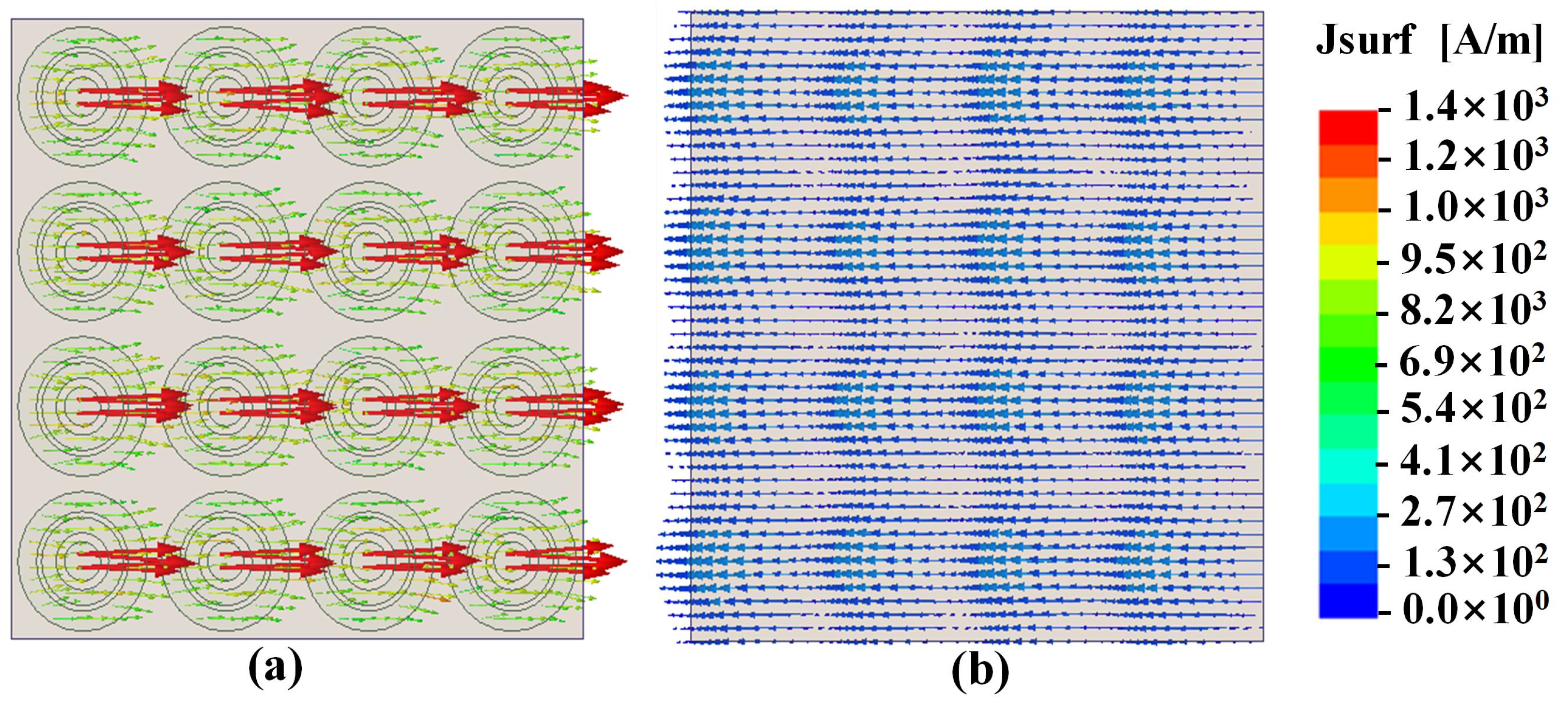
To reveal the mechanism inducing such high absorption, the electric field distribution and surface current distribution of the absorber will be provided. Simulated electric field distribution, surface current density of the first graphene layer and surface current density of the backed Au ground at THz are plotted in Figure 5. Apparently, electric resonance occurs in the edge of both the outer Annulus and the inner Annulus, and the transient current directions of the first graphene layer and the ground plane are just opposite, forming a magnetic dipole response at 3.8 THz. As for the second graphene layer, the absorption peak is obtained at THz with the absorption of 81.73%, as shown in Figure 2b. The surface current distribution on the second graphene layer and backed Au ground layer are next investigated to further explore the high spectrum absorption. Obviously, there exists an electric resonance on each super unit cell, as depicted in Figure 6 and Figure 7 offers that the directions of transient current of the second graphene layer and the ground plane are also reversed, emerging the magnetic dipole response at 6 THz.
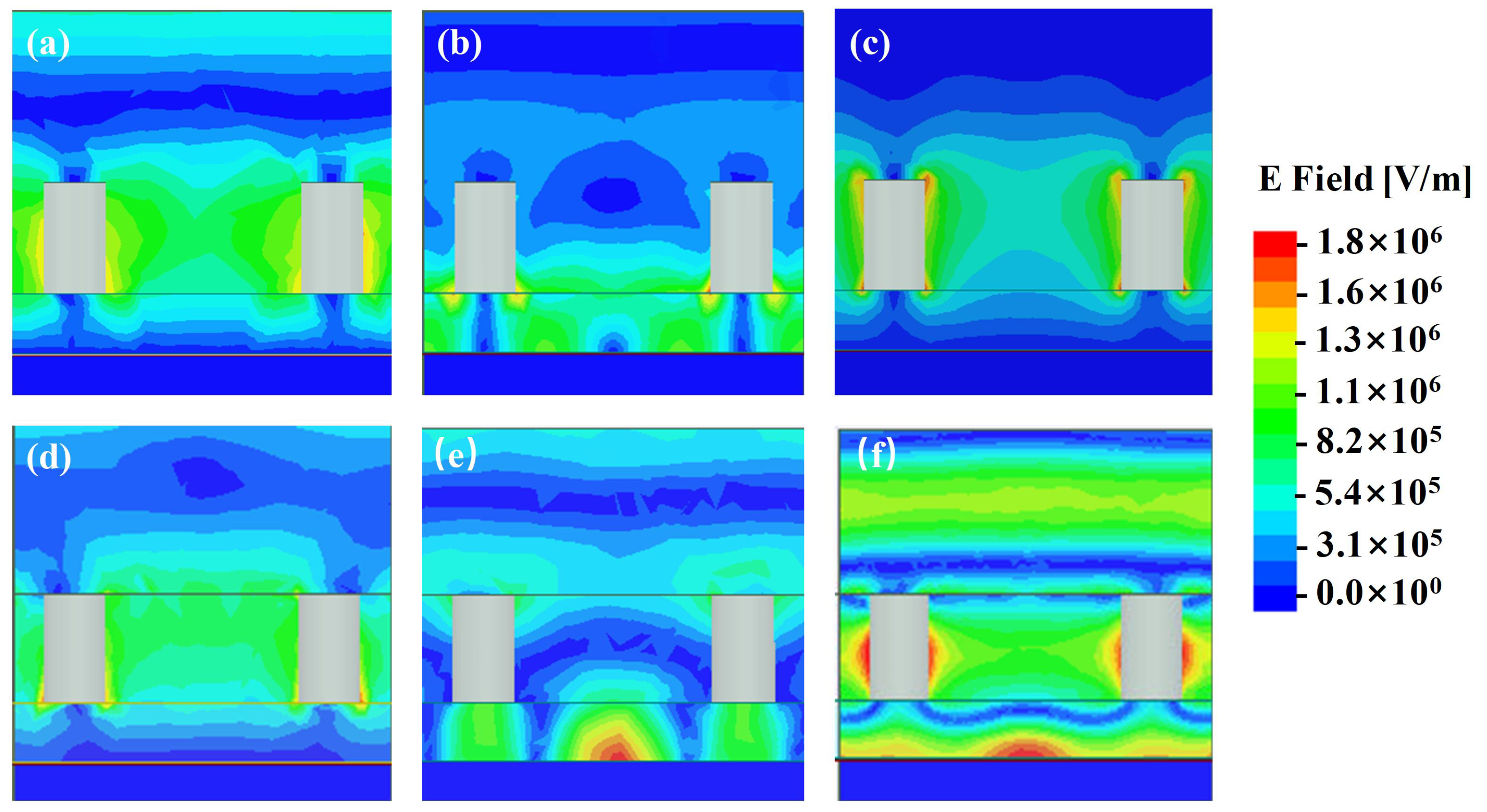
To further explain the mechanism of improved absorption, electromagnetic field profile for the structures with and without graphene are delineated, as shown in Figure 8. At 3.7 THz, it is easy to find that few changes appear, the absorption holds normal at lower spectrum. At 6.5 THz, we can catch the sight of local electric field enhancement, which could explain the ascendant absorption at higher spectrum. In addition, at 7.6 THz, upon the basis of cylinders’ resonance, interaction within graphene and metal columns is perceived, with improved absorption rate of high spectrum. Compared with the recently reported THz broadband absorber with a bandwidth of 3.31 THz while absorption exceeding 50% [25], the bandwidth of our proposed absorber has wider bandwidth of 7.1 THz and higher absorption of 80%. Furthermore, the electrically tunable property of the ultra-broadband absorber is investigated. The surface conductivity of graphene sheet relates largely to its Fermi energy, which can be controlled by electrostatic doping or applying bias voltage. Through varying the Fermi level of the graphene sheet located on the separate layer, the absorption amplitude of low spectrum and high spectrum can be independently controlled with almost unchanging influence of adjacent band, as shown in Figure 9. It should be noted that through changing the chemical potential of graphene, the conductivity of graphene can be changed correspondingly. Thus by tuning the chemical potential of graphene can indirectly change impedance matching. Trough changing the impedance matching, we can flexibly obtain the demanding absorption bandwidth. When the chemical potential of the first layer goes down, the absorption for the simulated frequency response of the lower spectrum goes down too, vice versa. In addition, when the chemical potential of the second layer goes down, the absorption for the simulated frequency response of the upper spectrum goes down too. Only when we choose the optimized value of combination of the two variables, , , can we get the optimal bandwidth.
Next, we will discuss the characteristics of independence of polarization angle. The polarization angle is defined as included angle between x-axis and electric vector of plane wave. In the above mentioned analysis, we discussed the characteristics only under normal incidence scenario. We have investigated the absorption consistency of variational trend under the changes of the polarization angle ranging from to in steps of , at varying incidence angle from to , with a step width of . As shown in Figure 10, little variance of absorbance emerges for the structure, illustrating highly consistent absorption performance under various polarization angles of incident plane wave. In other words, the absorption performance of the structure is independent of polarization. It has a great advantage in many THz applications where non-polarized source is preferred to achieve high absorption efficiency.
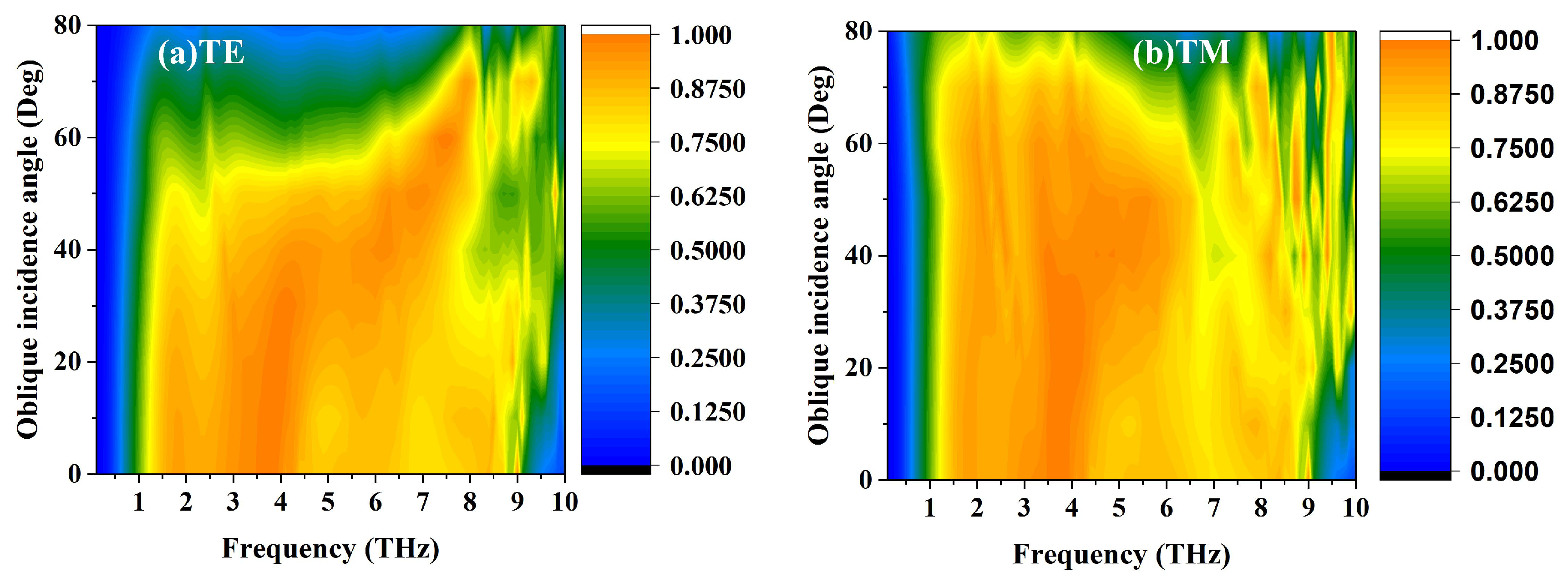
Additionally, the absorption spectrum under varied oblique incidence in both the TE and TM modes are studied, as depicted in Figure 11a,b, respectively. In the simulation, the incidence angles vary from to with the step width of . It can be presented that the peak absorption keeps larger than 70% up to incidence angles for both the TE mode and the TM mode, respectively.
In addition, regarding the angular stability study, both TE- and TM-polarized incident plane waves are considered. The angular stability of the proposed absorber under oblique incidence is determined by the thickness of the metallic cylinders and the substrate, the geometry and the size of the unit-cell (periodicity) compared to the whole thickness of the structure [31]. However, it should be aware that these factors not only influence the angular stability but also the absorbing bandwidth. It can be explained from Figure 3, the impedance of is related to the thickness of the metallic cylinders and has relation with the thickness of the substrate. Changing and can affect the input impedance of the whole structure, further influencing the absorbing bandwidth. Thus, a trade-off solution has to be optimized for the values of the thickness and the absorption bandwidth. Commercial Software HFSS of Ansoft based on finite elements methods (FEM) and Quasi Newton algorithm are chosen to achieve the optimization process. First, we set the incidence angle (theta) varied from to in steps of , at varying polarization angles from to , with a step width of . The comparison is implemented in terms of the absolute bandwidth, comprising the frequencies for which the absorption of the structure keeps higher than 70%, no matter the phi and theta angles in the considered range. As shown in Table 1 and Table 2, when theta is lower than , the bandwidth has wide bandwidth with absorption higher than 70%. In addition, when the theta angle is higher than , it is obvious that the absorption bandwidth reduces.
As shown in Figure 10, for different oblique illuminations, we can clearly find that when the incident angle is above , the bandwidth with absorption higher than 70% reduced a lot. It may be explained that the sheet impedance of graphene does not change with the incident angle and polarization states, but as the incident angle of plane wave changes, projection impedance of incident wave varies, the impedance mismatch becomes worse. So the meta-absorber has an incident angle about with broadband absorption higher than 70%.
Finally, we have achieved a bilayer graphene-based absorption structure with Au cylinder arrays on parylene substrate. It can achieve high absorption rate of 80% within 7.1 THz with polarization-insensitive both TE and TM polarizations, and an incident-angle about with broadband absorption higher than 70%.
5. Conclusions
In summary, a bilayer graphene-based absorption structure with Au cylinder arrays on parylene substrate is proposed and numerically simulated at THz wavelengths. We use the cascading bilayer graphene structure with two different frequency resonances. The first graphene layer achieves wave absorption in low frequency band, the second graphene layer achieves wave absorption in high frequency band. Ultra-wideband is realized when the guided resonance is excited in the Au cylinder array, promoting input impedance of the whole structure to closely match with the free space, connecting the low frequency and high frequency absorption bands and broadening the whole spectrum. The bandwidth and resonance position of the absorption resonance can be independently tuned by varying the chemical potential of separate graphene layers. Simulation results demonstrate that the absorption of the proposed structure can be as high as more than 80% from 2.9 THz to 7.1 THz with variation of the graphene’s chemical potential from 0.2 to 0.97 with polarization insensitive for both TE and TM polarizations stable against frequency.
Author Contributions
Conceptualization, S.L. (Shuxiang Liu) and L.D.; methodology, S.L. (Shuxiang Liu); software, S.L. (Shuxiang Liu); validation, S.L. (Shuxiang Liu); formal analysis, S.L. (Shuxiang Liu); investigation, S.L. (Shuxiang Liu); resources, L.D. and S.L. (Shufang Li); data curation, S.L. (Shuxiang Liu); writing—original draft preparation, S.L. (Shuxiang Liu); writing—review and editing, S.L. (Shuxiang Liu), M.Q. and S.L. (Shufang Li); visualization, S.L. (Shuxiang Liu); supervision, L.D.; project administration, L.D. and S.L. (Shufang Li); funding acquisition, L.D. and S.L. (Shufang Li).
Funding
This research was funded by National Nature Science Foundation of China No. 61601040 and 61427801.
Acknowledgments
This work was supported by National Nature Science Foundation of China (No. 61601040 and 61427801), 111 project (No. B17007) and Director Funds of Beijing Key Laboratory of Network System Architecture and Convergence (No. 2017BKL-NSAC-ZJ-01), Beijing Nova Program (No. Z181100006218039).
Conflicts of Interest
The authors declare no conflict of interest.
References
- Zhang, C.; Huang, C.; Pu, M.; Song, J.; Zhao, Z.; Wu, X.; Luo, X. Dual-band wide-angle metamaterial perfect absorber based on the combination of localized surface plasmon resonance and Helmholtz resonance. Sci. Rep. 2017, 7, 5652. [Google Scholar] [CrossRef] [PubMed]
- Stantchev, R.I.; Phillips, D.B.; Hobson, P.; Hornett, S.M.; Padgett, M.J.; Hendry, E. Compressed sensing with near-field THz radiation. Optica 2017, 4, 989–992. [Google Scholar] [CrossRef] [Green Version]
- Chen, M.; Singh, L.; Xu, N.; Singh, R.; Zhang, W.; Xie, L. Terahertz sensing of highly absorptive water-methanol mixtures with multiple resonances in metamaterials. Opt. Express 2017, 25, 14089–14097. [Google Scholar] [CrossRef] [PubMed]
- Tao, H.; Landy, N.I.; Bingham, C.M.; Zhang, X.; Averitt, R.D.; Padilla, W.J. A metamaterial absorber for the terahertz regime: Design, fabrication and characterization. Opt. Express 2008, 16, 7181–7188. [Google Scholar] [CrossRef] [PubMed]
- Cong, L.; Xu, N.; Zhang, W.; Singh, R. Polarization Control in Terahertz Metasurfaces with the Lowest Order Rotational Symmetry. Adv. Opt. Mater. 2015, 3, 1176–1183. [Google Scholar] [CrossRef]
- Yen, T.J.; Padilla, W.J.; Fang, N.; Vier, D.C.; Smith, D.R.; Pendry, J.B.; Basov, D.N.; Zhang, X. Terahertz magnetic response from artificial materials. Science 2004, 303, 1494–1496. [Google Scholar] [CrossRef] [PubMed]
- Zhang, S.; Park, Y.S.; Li, J.; Lu, X.; Zhang, W.; Zhang, X. Negative refractive index in chiral metamaterials. Phys. Rev. Lett. 2009, 102, 023901. [Google Scholar] [CrossRef] [PubMed]
- Singh, R.; Plum, E.; Zhang, W.; Zheludev, N.I. Highly tunable optical activity in planar achiral terahertz metamaterials. Opt. Express 2010, 18, 13425–13430. [Google Scholar] [CrossRef] [PubMed]
- Bahk, Y.M.; Kang, B.J.; Kim, Y.S.; Kim, J.Y.; Kim, W.T.; Kim, T.Y.; Kang, T.; Rhie, J.; Han, S.; Park, C.H.; et al. Electromagnetic saturation of angstrom-sized quantum barriers at terahertz frequencies. Phys. Rev. Lett. 2015, 115, 125501. [Google Scholar] [CrossRef]
- Yoshida, K.; Shibata, K.; Hirakawa, K. Terahertz field enhancement and photon-assisted tunneling in single-molecule transistors. Phys. Rev. Lett. 2015, 115, 138302. [Google Scholar] [CrossRef]
- Ju, L.; Geng, B.; Horng, J.; Girit, C.; Martin, M.; Hao, Z.; Bechtel, H.A.; Liang, X.; Zettl, A.; Shen, Y.R.; et al. Graphene plasmonics for tunable terahertz metamaterials. Nat. Nanotechnol. 2011, 6, 630. [Google Scholar] [CrossRef] [PubMed]
- Cheng, Y.; Gong, R.; Cheng, Z. A photoexcited broadband switchable metamaterial absorber with polarization-insensitive and wide-angle absorption for terahertz waves. Opt. Commun. 2016, 361, 41–46. [Google Scholar] [CrossRef]
- Jiang, Y.; Wan, X.; Wang, J.; Wang, J. Tunable Terahertz Absorber Based on Bulk-Dirac-Semimetal Metasurface. IEEE Photonics J. 2018, 10, 1–7. [Google Scholar] [CrossRef]
- Zhang, J.; Tian, J.; Li, L. A Dual-Band Tunable Metamaterial Near-Unity Absorber Composed of Periodic Cross and Disk Graphene Arrays. IEEE Photonics J. 2018, 10, 1–12. [Google Scholar] [CrossRef]
- Deng, G. Triple-band polarisation-independent metamaterial absorber at mm wave frequency band. IET Microw. Antennas Propag. 2018, 12, 1120–1125. [Google Scholar] [CrossRef]
- Huang, X.; Lu, C.; Rong, C.; Hu, Z.; Liu, M. Multiband Ultrathin Polarization-Insensitive Terahertz Perfect Absorbers With Complementary Metamaterial and Resonator Based on High-Order Electric and Magnetic Resonances. IEEE Photonics J. 2018, 10, 1–11. [Google Scholar] [CrossRef]
- Dorche, A.E.; Abdollahramezani, S.; Chizari, A.; Khavasi, A. Broadband, Polarization-Insensitive, and Wide-Angle Optical Absorber Based on Fractal Plasmonics. IEEE Photonics Technol. Lett. 2016, 28, 2545–2548. [Google Scholar] [CrossRef] [Green Version]
- Zhang, Y.; Li, Y.; Cao, Y.; Liu, Y.; Zhang, H. Graphene induced tunable and polarization-insensitive broadband metamaterial absorber. Opt. Commun. 2017, 382, 281–287. [Google Scholar] [CrossRef]
- Guo, W.; Liu, Y.; Han, T. Ultra-broadband infrared metasurface absorber. Opt. Express 2016, 24, 20586–20592. [Google Scholar] [CrossRef]
- Xiong, H.; Wu, Y.B.; Dong, J.; Tang, M.C.; Jiang, Y.N.; Zeng, X.P. Ultra-thin and broadband tunable metamaterial graphene absorber. Opt. Express 2018, 26, 1681–1688. [Google Scholar] [CrossRef]
- Torabi, E.S.; Fallahi, A.; Yahaghi, A. Evolutionary Optimization of Graphene-Metal Metasurfaces for Tunable Broadband Terahertz Absorption. IEEE Trans. Antennas Prog. 2017, 65, 1464–1467. [Google Scholar] [CrossRef] [Green Version]
- Dong, Y.; Liu, P.; Yu, D.; Li, G.; Yang, L. A Tunable Ultrabroadband Ultrathin Terahertz Absorber Using Graphene Stacks. IEEE Antennas Wirel. Propag. Lett. 2017, 16, 1115–1118. [Google Scholar] [CrossRef]
- Fardoost, A.; Vanani, F.G.; Safian, R. Design of a Multilayer Graphene-Based Ultrawideband Terahertz Absorber. IEEE Trans. Nanotechnol. 2017, 16, 68–73. [Google Scholar]
- Pan, W.; Yu, X.; Zhang, J.; Zeng, W. A Novel Design of Broadband Terahertz Metamaterial Absorber Based on Nested Circle Rings. IEEE Photonics Technol. Lett. 2016, 28, 2335–2338. [Google Scholar] [CrossRef]
- Jia, D.; Xu, J.; Yu, X. Ultra-broadband terahertz absorption using bi-metasurfaces based multiplexed resonances. Opt. Express 2018, 26, 26227. [Google Scholar] [CrossRef] [PubMed]
- Sayem, A.A.; Mahdy, M.R.C.; Rahman, M.S. Broad angle negative refraction in lossless all dielectric or semiconductor based asymmetric anisotropic metamaterial. J. Opt. 2016, 18, 015101. [Google Scholar] [CrossRef]
- Cong, L.; Pitchappa, P.; Wu, Y.; Ke, L.; Lee, C.; Singh, N.; Yang, H.; Singh, R. Active Multifunctional Microelectromechanical System Metadevices: Applications in Polarization Control, Wavefront Deflection, and Holograms. Adv. Opt. Mat. 2016, 5, 1600716. [Google Scholar] [CrossRef]
- Cong, L.; Tan, S.; Yahiaoui, R.; Yan, F.; Zhang, W.; Singh, R. Experimental demonstration of ultrasensitive sensing with terahertz metamaterial absorbers: A comparison with the metasurfaces. Appl. Phys. Lett. 2015, 106, 031107. [Google Scholar] [CrossRef]
- Cong, L.; Pitchappa, P.; Lee, C.; Singh, R. Active Phase Transition via Loss Engineering in a Terahertz MEMS Metamaterial. Adv. Mater. 2017, 29, 1700733. [Google Scholar] [CrossRef]
- Liu, N.; Liu, H.; Zhu, S.; Giessen, H. Stereometamaterials. Nat. Photonics 2009, 3, 157–162. [Google Scholar] [CrossRef]
- De Cos, M.E.; Las-Heras, F. On the advantages of loop-based unit-cell’s metallization regarding the angular stability of artificial magnetic conductors. Appl. Phys. A 2015, 118, 699–708. [Google Scholar] [CrossRef]
Figure 1.
Proposed meta-absorber with bilayer graphene and Au cylinders. (a) Schematic of the proposed absorber. (b) Top view of the unit cell of top layer, (c) Top view of the unit cell of second graphene layer.
Figure 1.
Proposed meta-absorber with bilayer graphene and Au cylinders. (a) Schematic of the proposed absorber. (b) Top view of the unit cell of top layer, (c) Top view of the unit cell of second graphene layer.

Figure 2.
(a) Boundary and Excitation setting for the unit cell of the proposed absorber, (b) The simulated frequency responses for Line 1: with the first graphene layer, Line 2: with the second graphene layer, Line 3: the proposed absorber, Line 4: without the cylinders array.
Figure 2.
(a) Boundary and Excitation setting for the unit cell of the proposed absorber, (b) The simulated frequency responses for Line 1: with the first graphene layer, Line 2: with the second graphene layer, Line 3: the proposed absorber, Line 4: without the cylinders array.

Figure 3.
The diagrammatic sketch of an equivalent circuit model of the proposed absorber.

Figure 4.
(a) Comparison of input impedance with cylinders array and with parylene substrate. (b) The simulated frequency responses with different .
Figure 4.
(a) Comparison of input impedance with cylinders array and with parylene substrate. (b) The simulated frequency responses with different .

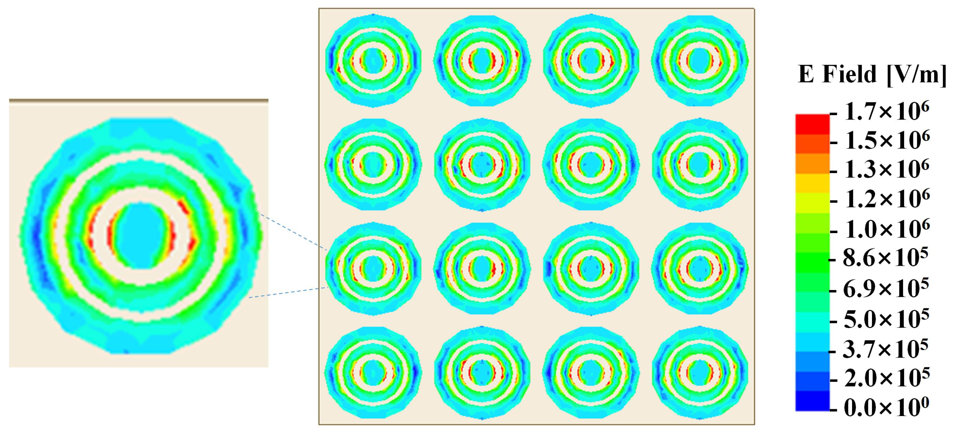
Figure 5.
The simulated (a) electric field distribution and (b) surface current density of the first graphene layer and (c) surface current density of the backed Au ground at THz.
Figure 5.
The simulated (a) electric field distribution and (b) surface current density of the first graphene layer and (c) surface current density of the backed Au ground at THz.

Figure 6.
The simulated electric field distribution of the second graphene layer at THz.

Figure 7.
The simulated surface current density of (a) the second graphene layer and (b) the backed ground at the frequency of THz.
Figure 7.
The simulated surface current density of (a) the second graphene layer and (b) the backed ground at the frequency of THz.

Figure 8.
The electromagnetic field profile for the structures, (a) without graphene at 3.7 THz, (b) without graphene at 6.5 THz, (c) without graphene at 7.6 THz, (d) with graphene at 3.7 THz, (e) with graphene at 6.5 THz, (f) with graphene at 7.6 THz.
Figure 8.
The electromagnetic field profile for the structures, (a) without graphene at 3.7 THz, (b) without graphene at 6.5 THz, (c) without graphene at 7.6 THz, (d) with graphene at 3.7 THz, (e) with graphene at 6.5 THz, (f) with graphene at 7.6 THz.

Figure 9.
The simulated absorption spectrum with changing graphene loading voltage of (a) the first graphene layer, (b) the second graphene layer.
Figure 9.
The simulated absorption spectrum with changing graphene loading voltage of (a) the first graphene layer, (b) the second graphene layer.

Figure 10.
Simulated absorption spectra of the absorber for different polarization angles under various incidence.
Figure 10.
Simulated absorption spectra of the absorber for different polarization angles under various incidence.

Figure 11.
Absorption contour map of the absorber under various incident angles (a) TE mode and (b) TM mode.
Figure 11.
Absorption contour map of the absorber under various incident angles (a) TE mode and (b) TM mode.


Table 1.
Absorption bandwidth under the changes of the incident angle theta for TE incident wave.
| Bandwidth (THz) | phi = | phi = | phi = | phi = | phi = |
|---|---|---|---|---|---|
| theta = | 7.3 | 7.4 | 7.3 | 7.4 | 7.4 |
| theta = | 7.4 | 7.5 | 7.4 | 7.4 | 7.5 |
| theta = | 7.6 | 7.7 | 7.6 | 7.6 | 7.7 |
| theta = | 7.9 | 7.9 | 7.9 | 7.9 | 7.9 |
| theta = | 8.3 | 8.0 | 8.3 | 8.1 | 6.7 |
| theta = | 6.2 | 4.3 | 6.2 | 4.9 | 4.7 |
| theta = | 2.7 | 2.4 | 2.7 | 2.5 | 1.8 |
| theta = | 1.3 | 1.0 | 1.3 | 1.2 | 0.9 |
Table 2.
Absorption bandwidth under the changes of the incident angle theta for TM incident wave.
| Bandwidth (THz) | phi = | phi = | phi = | phi = | phi = |
|---|---|---|---|---|---|
| theta = | 7.3 | 7.4 | 7.3 | 7.4 | 7.4 |
| theta = | 7.4 | 7.5 | 7.4 | 7.4 | 7.5 |
| theta = | 7.6 | 7.8 | 7.6 | 7.6 | 7.7 |
| theta = | 8.2 | 8.0 | 8.2 | 8.2 | 7.9 |
| theta = | 8.4 | 8.6 | 8.4 | 8.6 | 7.8 |
| theta = | 8.6 | 8.3 | 8.6 | 6.9 | 8.1 |
| theta = | 7.4 | 8.0 | 7.4 | 7.5 | 7.6 |
| theta = | 3.9 | 3.4 | 3.9 | 3.5 | 3.5 |
© 2019 by the authors. Licensee MDPI, Basel, Switzerland. This article is an open access article distributed under the terms and conditions of the Creative Commons Attribution (CC BY) license (http://creativecommons.org/licenses/by/4.0/).
Share and Cite
MDPI and ACS Style
Liu, S.; Deng, L.; Qu, M.; Li, S. Polarization-Independent Tunable Ultra-Wideband Meta-Absorber in Terahertz Regime. Electronics 2019, 8, 831. https://doi.org/10.3390/electronics8080831
AMA Style
Liu S, Deng L, Qu M, Li S. Polarization-Independent Tunable Ultra-Wideband Meta-Absorber in Terahertz Regime. Electronics. 2019; 8(8):831. https://doi.org/10.3390/electronics8080831
Chicago/Turabian StyleLiu, Shuxiang, Li Deng, Meijun Qu, and Shufang Li. 2019. "Polarization-Independent Tunable Ultra-Wideband Meta-Absorber in Terahertz Regime" Electronics 8, no. 8: 831. https://doi.org/10.3390/electronics8080831
Note that from the first issue of 2016, this journal uses article numbers instead of page numbers. See further details here.