Design of Broadband W-Band Waveguide Package and Application to Low Noise Amplifier Module


Department of Electronic Engineering, Sogang University, Seoul 04107, Korea
*
Author to whom correspondence should be addressed.
Electronics 2019, 8(5), 523; https://doi.org/10.3390/electronics8050523
Submission received: 27 April 2019
/
Revised: 8 May 2019
/
Accepted: 8 May 2019
/
Published: 10 May 2019
(This article belongs to the Special Issue Millimeter-Wave (mmWave) Communications)
Abstract
:In this paper, the broadband millimeter-wave waveguide package, which can cover the entire W-band (75–110 GHz) is presented and applied to build a low noise amplifier module. For this purpose, a broadband waveguide-to-microstrip transition was designed using an extended E-plane probe in a low-loss and thin dielectric substrate. The end of the probe substrate was firmly fixed on to the waveguide wall in order to minimize the performance degradation caused by the probable bending of the substrate. In addition, we predicted and analyzed in-band resonances by the simulations that are caused by the empty spaces in the waveguide package to accommodate integrated circuits (ICs) and external bias circuits. These resonances are removed by designing an asymmetrical bias space structure with a radiation boundary at an external bias connection plane. The bond-wires, which are used to connect the ICs with the transition, can generate impedance mismatches and limit the bandwidth performance of the waveguide package. Their effect is carefully compensated for by designing the broadband two-section matching circuits in the transition substrate. Finally, the broadband waveguide package is designed using a commercial three-dimensional electromagnetic structure simulator and applied to build a W-band low noise amplifier module. The measurement of the back-to-back connected waveguide-to-microstrip transition including the empty spaces for the ICs and bias circuits showed the insertion loss less than 3.5 dB and return loss higher than 13.3 dB across the entire W-band without any in-band resonances. The measured insertion loss includes the losses of 8.7 mm-long microstrip line and 41.8 mm-long waveguide section. The designed waveguide package was utilized to build the low noise amplifier module that had a measured gain greater than 14.9 dB from 75 GHz to 105 GHz (>12.9 dB at the entire W-band) and noise figure less than 4.4 dB from 93.5 GHz to 94.5 GHz.
1. Introduction
Millimeter-wave frequencies including W-band (75–110 GHz) have short wavelengths and broad allocated bandwidth, which are beneficial for high resolution radars and high speed wireless communications [1,2,3,4,5]. In the millimeter-wave frequency range, a rectangular waveguide is generally adopted as a main transmission line instead of a coaxial cable due to the lower loss and easier manufacturability [6]. Therefore, millimeter-wave circuits including integrated circuits (ICs) should be packaged in the rectangular waveguide. This waveguide package needs to be designed to have broadband and low-loss performance. However, there are several design issues to be solved for high performance millimeter-wave waveguide packages [6,7].
The rectangular waveguide has a dominant electromagnetic (EM) field mode of a transverse electric (TE10), so that broadband waveguide-to-microstrip transition is an essential component in order to package the ICs in a microstrip [8,9,10,11,12,13,14,15,16,17,18,19]. In addition, the empty spaces inside the metallic waveguide are required to accommodate ICs and their bias circuits, and they form metallic cavities that can generate in-band resonances, seriously degrading the performance of the waveguide packages [11,12]. Finally, bond-wires, which are generally used to electrically connect the ICs to the transition, can produce impedance mismatches and limit the bandwidth performance, especially at millimeter-wave frequencies. Therefore, their effect should be accurately modeled and corrected not to degrade the performance when the IC is packaged in the waveguide [20].
In this work, we present the broadband waveguide package at W-band, by designing a broadband low-loss waveguide-to-microstrip transition using an extended E-plane probe, analyzing and removing the in-band resonances caused by the cavities in the waveguide package, and designing broadband bond-wire compensation circuits. These in-band resonance problems and the bond-wire compensation circuits have not been deeply treated in the previous publications on W-band waveguide modules [21,22]. The waveguide package is designed and applied to build the broadband low noise amplifier (LNA) module. A three-dimensional (3-D) EM simulator is used in the analysis and design of the W-band waveguide package. The designed transition and LNA module are both fabricated to show the resonance-free broadband performance covering the entire W-band.
2. Design of Broadband W-band Waveguide Package
2.1. Waveguide-to-Microstrip Transition Using Extended E-Plane Probe
There has been extensive research in developing millimeter-wave waveguide transitions using E-plane probes [8,9], dipole antenna [10,11,12], antipodal finlines [13,14], and substrate integrated waveguides [15]. In this work, the E-plane probe transition was adopted because of its small size and low-loss performance, as shown in Figure 1. The transition substrate is placed in the central E-plane of waveguide and supported on the channel. The square metallic patch on the substrate captures and transforms EM fields in the TE10 mode of the waveguide to the quasi-transverse electromagnetic (TEM) mode of the microstrip line. The high impedance line is used to match the impedances of the probe to that of the microstrip line. In order to minimize the reflection from air-filled waveguide, very thin substrate with low dielectric constant (127 μm-thick TLY-5 with εr = 2.2 by Taconic) is used as a transition substrate, considering a small internal size of the standard W-band waveguide (WR-10: 2.54 mm × 1.27 mm). This very thin and soft substrate, however, can be easily bent by a small force during the packaging process, which can lead to serious performance degradation and poor repeatability. In order to alleviate these problems, the substrate in the probe section was extended to the other side of the waveguide and fixed into the slit [16].
The dimensions of the transition were determined by the commercial 3-D structure simulator (HFSS by Ansys in Canonsburg, PA, USA) and listed in Table 1. At first, the transition was designed without the slit region. Then, the slit was inserted in the simulation and the dimensions were slightly modified. The slit exhibits the marginal effect on the transition performance. Figure 2 shows the simulated performance of the designed transition. The insertion loss (–10log|S21|2) was less than 0.6 dB and return loss (–10log|S11|2) was higher than 21.6 dB across the whole W-band.
2.2. Resonances-Free Waveguide Package
The waveguide package with the transitions necessarily requires several empty spaces to accommodate the circuits, including ICs and direct current (DC) bias circuits. Figure 3 shows the waveguide package with the transitions to package the W-band LNA IC (size = 2 mm × 3 mm). The LNA IC will sit in the place of the microstrip line in the middle. There are several empty spaces for the circuits to supply DC bias to the LNA IC from external power supplies. Unfortunately, these empty spaces can form metallic cavities and generate parasitic resonances that can be observed in the EM simulations. Note that this waveguide package is all closed by the metal except for the waveguide input and output ports. The plane A can be either open or closed for the external bias supply connection.
Figure 4a shows the simulated performance of the waveguide package of Figure 3 (back-to-back transition with several empty spaces) with the plane A closed. There are many resonances at in-band frequencies at which insertion and return losses are seriously degraded. Figure 4c shows the electric field distribution at one of resonance frequencies (86.1 GHz). It can be stated from this figure that this resonance was generated in the empty spaces for the IC and bias circuits, which work as metallic cavities.
These resonances can be partly suppressed by applying a radiation boundary to the plane A instead of the metal boundary, as shown in Figure 4b. However, there still exists a few in-band resonances. At 76.0 GHz, the electric field distribution is drawn in Figure 4d, showing that the strong electric field was invoked in the IC space and leaked into the bias spaces. Both Figure 4c,d demonstrated that the resonances could be produced in the LNA space. Note that this space was enclosed by the metallic walls and the open boundaries as shown in Figure 4d, forming the rectangular cavity-like structure. The fields in this structure were excited by the microstrip line.
In order to get rid of all the in-band resonances, the LNA space was designed to have an asymmetrical structure as shown in Figure 5a, deforming the rectangular cavity-like structure. It can hinder an electric field from being concentrated in the IC space and thus suppress the resonances. Figure 5b shows the simulated S-parameters of the waveguide package with an asymmetrical structure (with the radiation boundary at the plane A), showing insertion loss less than 1.3 dB and return loss higher than 18.7 dB across the full W-band without any in-band resonances. Note that the insertion loss is that of the back-to-back transitions including the 8.7 mm-long microstrip line.
2.3. Compensation of Bond-Wire Effect
In general, bond-wires are used to electrically connect the IC with the microstrip line in the transition substrate. Their effect can be modeled using series inductances and shunt capacitances that can produce serious impedance mismatches, especially at millimeter-wave frequencies [20]. Figure 6a shows the bond-wire connection between 127 μm-thick substrate and 100 μm-thick GaAs substrate (εr = 12.9) with a 200 μm distance. A gold wire with a diameter of 25 μm was placed 40 μm above the copper microstrip line in the TLY-5 substrate. Figure 6c shows the simulated S-parameters at W-band showing the increased insertion loss and poor return loss by the bond-wire.
In order to reduce impedance mismatches by the bond-wire, a broadband compensation circuit was designed using two-section matching network as shown in Figure 6b. The simulation shows that the bond-wire can dramatically increase the impedance at W-band due to its parasitic inductance. This impedance could be lowered and matched to 50 Ω by using the circuit section consisting of an open stub and a high impedance line. A two-section matching network was employed to accomplish the broadband matching performance. Figure 6c demonstrated that the designed compensation circuit could recover the performance providing broadband impedance match and lower loss at the W-band. The mismatch increased at higher frequencies due to the increased impedance of the bond-wire. The simulated return loss was higher than 9.1 dB across the full W-band.
3. Experimental Results
3.1. W-Band Waveguide Transition
The designed W-band waveguide package was fabricated in an aluminum split-block configuration. Figure 7a shows the magnified view of the back-to-back transition including the empty spaces for the LNA IC and bias circuits. The transition substrate was mounted on the channel and its two ends were also fixed in the slit region using epoxy. Figure 7b presents the measurement results using a vector network analyzer (VNA; 8510C by Agilent in Santa Clara, CA, USA) with a W-band frequency extender. The simulation results were also plotted for the comparison. The simulation seemed to underestimate the losses by the microstrip line and waveguide sections. The measured return and insertion losses were better than 13.3 dB and 3.5 dB without any in-band resononaces, respectively, over the entire W-band. The insertion loss was lower than 2.6 dB from 75 GHz to 94 GHz. Note that the insertion loss included the loss of the 8.7 mm-long microstrip line and 41.8 mm-long waveguide section.
3.2. Bond-Wire Compensation Circuit
In order to verify the effectiveness of the designed bond-wire compensation circuit, the back-to-back transition shown in Figure 7a was slightly modified to have a bond-wire and its compensation circuit as shown in Figure 8a. The microstrip line in the middle would be replaced with the LNA IC later. The Duroid subtrate with the same dielectric constant and thickness to TLY-5 was used in this experiment. The measurement results are presented in Figure 8b, showing a wideband performance with an insertion loss less than 3.9 dB and return loss higher than 10.0 dB from 83.8 GHz to 95.7 GHz.
3.3. W-Band LNA Module
The fabricated waveguide package was used to build the W-band LNA module as shown in Figure 9. The overall package size was 50 mm × 30 mm × 50 mm. The commercially-available W-band LNA IC (by OMMIC in Paris, France) was mounted and bond-wired to the transition together with the designed bond-wire compensation circuits. Several capacitors were connected in shunt with gate and drain bias lines to suppress low frequency oscillations.
Figure 10a shows the S-parameters of the W-band LNA module measured by the VNA. It achieved the gain (10log|S21|2) higher than 14.9 dB from 75–105 GHz. It reduced to 12.9 dB at the band edge (110 GHz), which was caused by the LNA and bond-wire compensation circuit. Noise figure was also measured as shown in Figure 10b using a noise figure analyzer (N8975A by Agilent), W-band noise source (NC5110 by Noisecom in Parsippany-Troy Hills, NJ, USA), down-conversion mixer, and spectrum analyzer. The measurement bandwidth was limited to 1.0 GHz from 93.5 GHz to 94.5 GHz by the instruments, where the measured noise figure was less than 4.4 dB. This result appeared to be reasonable, considering the simulated noise figure of the LNA IC (2.8 dB given by the vendor) and the losses of the transitions and bond-wires. Note that the gain measured by the noise figure analyzer was very close to the one by VNA.
4. Conclusions
The broadband waveguide package covering the whole W-band was designed and implemented in this work. The broadband waveguide-to-microstrip transition was presented using an extended E-plane probe transition. The in-band resonances invoked by the cavities, which are formed by the empty spaces for IC and bias circuits, were predicted and removed by designing the asymmetrical structure with open boundary. The bond-wire effect was also simulated and its compensation circuit was designed to recover broadband performance. The fabricated W-band waveguide package exhibited the resonance-free broadband insertion and return losses. The LNA module using the developed waveguide package achieved broadband high gain with a low noise figure at W-band. These results verify that the designed waveguide package can be successfully utilized in the implementation of high performance W-band electronic modules and systems.
Author Contributions
Conceptualization, J.D., W.P. and J.J.; Methodology, W.P. and J.J.; Software, J.D. and W.P.; Validation, J.D. and W.C.; Formal Analysis, J.D.; Data Curation, J.D.; Writing-Original Draft Preparation, J.J.; Writing-Review & Editing, J.D. and J.J.; Visualization, J.D.; Supervision, J.J.; Funding Acquisition, J.J.
Funding
This work was partly supported by the Institute for Information & Communications Technology Planning & Evaluation (IITP) grant, funded by the Korean government (MSIT) (No. 2016-0-00185, Development of ultra-wideband terahertz CW spectroscopic imaging systems based on electronic devices). This work was also partly supported by a grant to the Terahertz Electronic Device Research Laboratory, funded by Defense Acquisition Program Administration and by the Agency for Defense Development (UD180025RD).
Conflicts of Interest
The authors declare no conflict of interest.
References
- Lee, S.; Joo, J.; Choi, J.; Kim, W.; Kwon, H.; Lee, S.; Kwon, Y.; Jeong, J. W-band multichannel FMCW radar sensor with switching-TX antennas. IEEE Sens. J. 2016, 16, 5572–5582. [Google Scholar] [CrossRef]
- Jeon, Y.; Bang, S. Front-End Module of 18–40 GHz Ultra-Wideband Receiver for Electronic Warfare System. J. Electromagn. Eng. Sci. 2018, 18, 188–198. [Google Scholar] [CrossRef]
- Li, X.; Xiao, J.; Yu, J. Long-Distance Wireless mm-Wave Signal Delivery at W-band. J. Lightwave Technol. 2016, 34, 661–668. [Google Scholar] [CrossRef]
- Lee, S.; Lee, S.; Park, H.; Kim, W.; Kwon, H.; Jeong, J.; Kwon, Y. W-band dual-channel receiver with active power divider and temperature-compensated circuit. Electr. Lett. 2016, 52, 850–851. [Google Scholar] [CrossRef]
- Shahramian, S.; Holyoak, M.J.; Baeyens, Y. A 16-Element W-band Phased-Array Transceiver Chipset With Flip-chip PCB Integrated Antennas for Multi-Gigabit Wireless Data Links. In Proceedings of the IEEE Radio Frequency Integrated Circuits Symposium (RFIC), Phoenix, AZ, USA, 17–19 May 2015; pp. 27–30. [Google Scholar] [CrossRef]
- Fujiwara, K.; Kobayashi, T. Low transmission loss, simple and broadband waveguide to microstrip line transducer in V-, E- and W-band. IEICE Electr. Express 2017, 14, 20170631. [Google Scholar] [CrossRef]
- Lee, S.; Son, D.; Kwon, J.; Park, Y. Analysis of a Tapered Rectangular Waveguide for V to W Millimeter Wavebands. J. Electromagn. Eng. Sci. 2018, 18, 248–253. [Google Scholar] [CrossRef]
- Ma, X.; Xu, R. A broadband W-band E-plane waveguide to microstrip probe transition. In Proceedings of the IEEE Asia Pacific Microwave Conference, Macau, China, 16–20 December 2008; pp. 1–4. [Google Scholar] [CrossRef]
- Li, E.S.; Tong, G.X.; Niu, D.C. Full W-band waveguide to microstrip transition with new E-plane probe. IEEE Microw. Wirel. Compon. Lett. 2013, 23, 4–6. [Google Scholar] [CrossRef]
- Choe, W.; Kim, J.; Jeong, J. Full H-band waveguide-to-coupled microstrip transition using dipole antenna with directors. IEICE Electr. Express 2017, 14, 1–6. [Google Scholar] [CrossRef]
- Kim, J.; Choe, W.; Jeong, J. Submillimeter-Wave Waveguide-to-Microstrip Transitions for Wide Circuits/Wafers. IEEE Trans. Terahertz Sci. Technol. 2017, 7, 440–445. [Google Scholar] [CrossRef]
- Choe, W.; Jeong, J. A Broadband THZ On-Chip Transition Using a Dipole Antenna with Integrated Balun. Electronics 2018, 7, 236. [Google Scholar] [CrossRef]
- Jeong, J.; Kin, D.; Kim, S.; Kwon, Y. V-band High-Efficiency Broadband Power Combiner and Power-Combining module Using Double Antipodal Finline Transitions. Electr. Lett. 2003, 39, 378–379. [Google Scholar] [CrossRef]
- Ki, H. A Study on Waveguide to Microstrip Antipodal Transition for 5 G Cellular Systems. J. Inst. Internet Broadcast. Commun. (JIIBC) 2015, 15. [Google Scholar] [CrossRef]
- Zhang, Y.; Shi, S.; Martin, R.D.; Prather, D.W. Broadband SIW to waveguide transition in multilayer LCP substrates at W band. IEEE Microw. Wirel. Compon. Lett. 2017, 224–226. [Google Scholar] [CrossRef]
- Park, W.; Choe; Lee, K.; Kwon, J.; Jeong, J. Millimeter-wave waveguide transducer using extended E-plane probe. J. Inst. Internet Broadcast. Commun (JIIBC) 2018, 18, 159–165. [Google Scholar] [CrossRef]
- Ariffin, A.; Isa, D.; Malekmohammadi, A. Broadband Transition from Microstrip Line to Waveguide Using a Radial Probe and Extended GND Planes for Millimeter-Wave Applications. PIER Lett. 2016, 60, 95–100. [Google Scholar] [CrossRef]
- Aljarosha, A.; Zaman, A.U. A Wideband Contactless and Bondwire-Free MMIC to Waveguide Transition. IEEE Microw. Wirel. Compon. Lett. 2017, 27, 437–439. [Google Scholar] [CrossRef]
- Hassan, E.; Noreland, D.; Wadbro, E.; Berggren, M. Topology Optimisation of Wideband Coaxial-to-Waveguide Transitions. Sci. Rep. 2017, 7. [Google Scholar] [CrossRef] [PubMed]
- Almenti, F.; Mezzanotte, P.; Roselli, L.; Sorrentino, R. An Equivalent Circuit for the Double Bonding Wire Interconnection. In Proceedings of the IEEE MTT-S International Microwave Symposium Digest, Anaheim, CA, USA, 13–19 June 1999; pp. 633–636. [Google Scholar]
- Zhou, P.; Zheng, P.; Yu, W.; Sun, H. Design of A W-band Low Noise Amplifier Module With MMIC. In Proceedings of the 2012 5th Global Symposium on Millimeter-Waves, Harbin, China, 27–30 May 2012; pp. 5–8. [Google Scholar] [CrossRef]
- Hua, Z.; Hongfei, Y.; Peng, D.; Yongbo, S.; Xiaoxi, N.; Zhi, J.; Xinyu, L. A full W-band low noise amplifier module for millimeter-wave applications. J. Semicond. 2015, 36, 095001. [Google Scholar] [CrossRef]
Figure 1.
Extended E-plane probe transition: (a) 3-D view and (b) cross-sectional view.
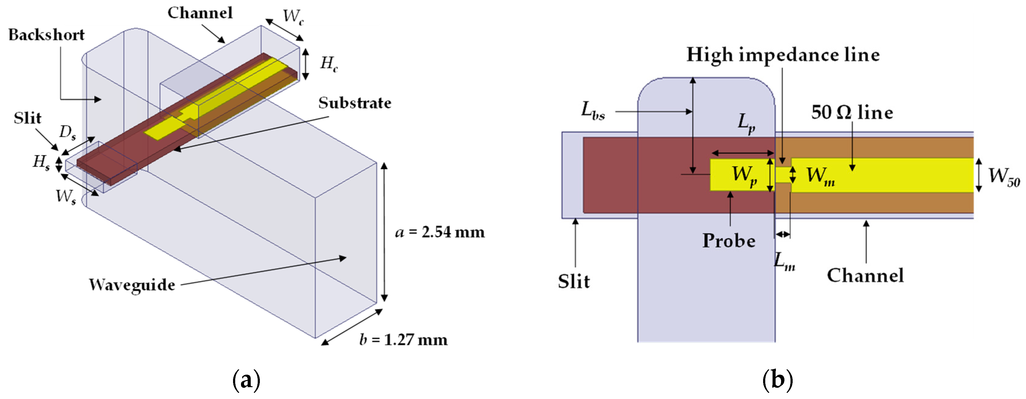
Figure 2.
Simulated S-parameters of the designed E-plane probe transition.

Figure 3.
Waveguide package for the low noise amplifier integrated circuit (LNA IC): (a) 3-D view and (b) cross-sectional view.
Figure 3.
Waveguide package for the low noise amplifier integrated circuit (LNA IC): (a) 3-D view and (b) cross-sectional view.
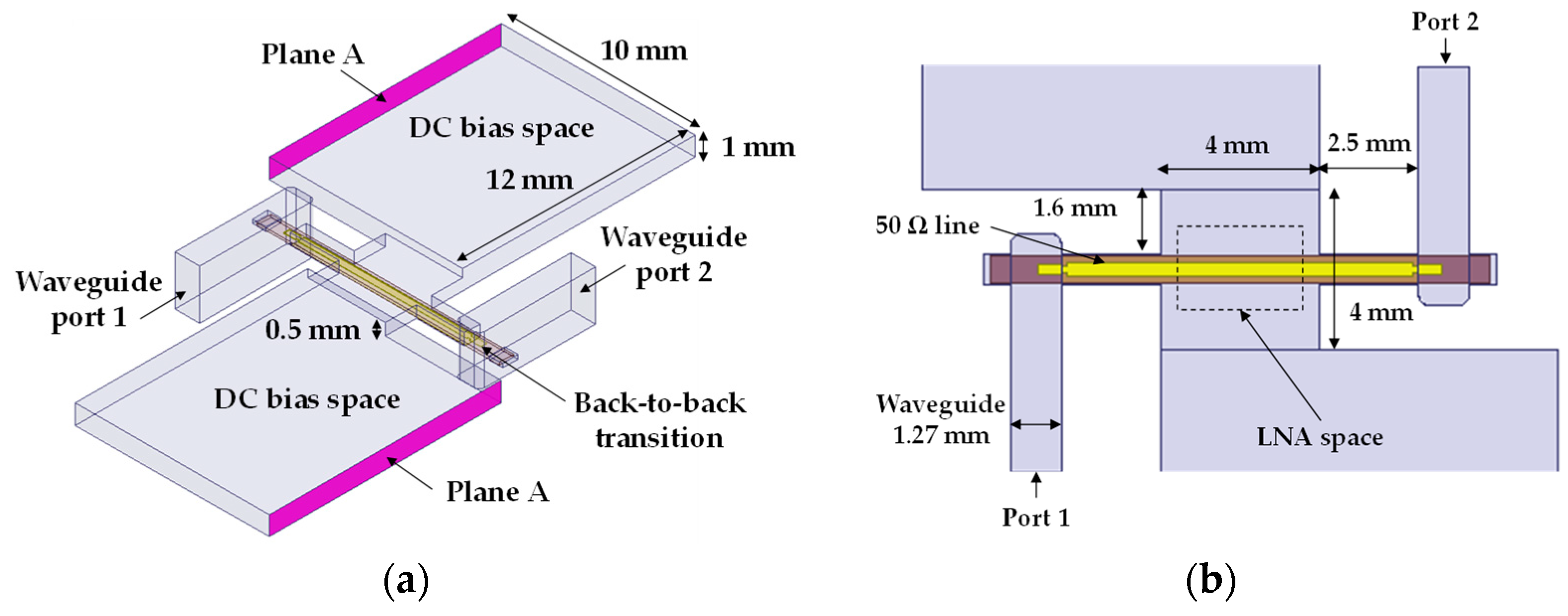
Figure 4.
Simulation of the waveguide package shown in Figure 3. (a) S-parameters with a metal boundary at plane A. (b) S-parameters with a radiation boundary at plane A. (c) Electric field distribution at 86.1 GHz (with a metal boundary at plane A). (d) Electric field distribution at 76.0 GHz (with a radiation boundary at plane A).

Figure 5.
Waveguide package with asymmetrical structure. (a) Cross-sectional view. (b) Simulated S-parameters.
Figure 5.
Waveguide package with asymmetrical structure. (a) Cross-sectional view. (b) Simulated S-parameters.
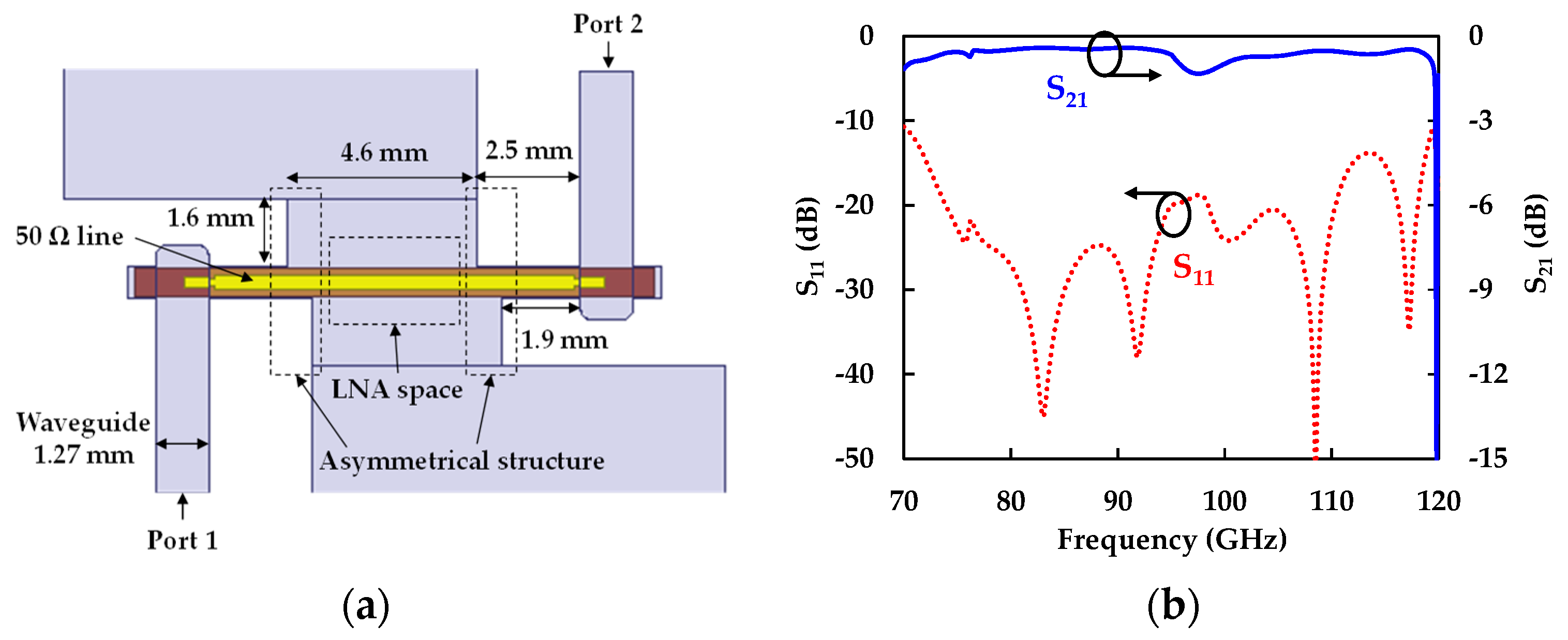
Figure 6.
Bond-wire simulation. (a) Basic structure of bond-wire connection. (b) Bond-wire compensation circuit. (c) Simulated S-parameters with compensation circuit (solid) and without compensation circuit (dotted).
Figure 6.
Bond-wire simulation. (a) Basic structure of bond-wire connection. (b) Bond-wire compensation circuit. (c) Simulated S-parameters with compensation circuit (solid) and without compensation circuit (dotted).

Figure 7.
Fabricated W-band transition including the empty spaces for the IC and bias circuits. (a) Photograph. (b) Measured (solid) and simulated (dotted) S-parameters.
Figure 7.
Fabricated W-band transition including the empty spaces for the IC and bias circuits. (a) Photograph. (b) Measured (solid) and simulated (dotted) S-parameters.
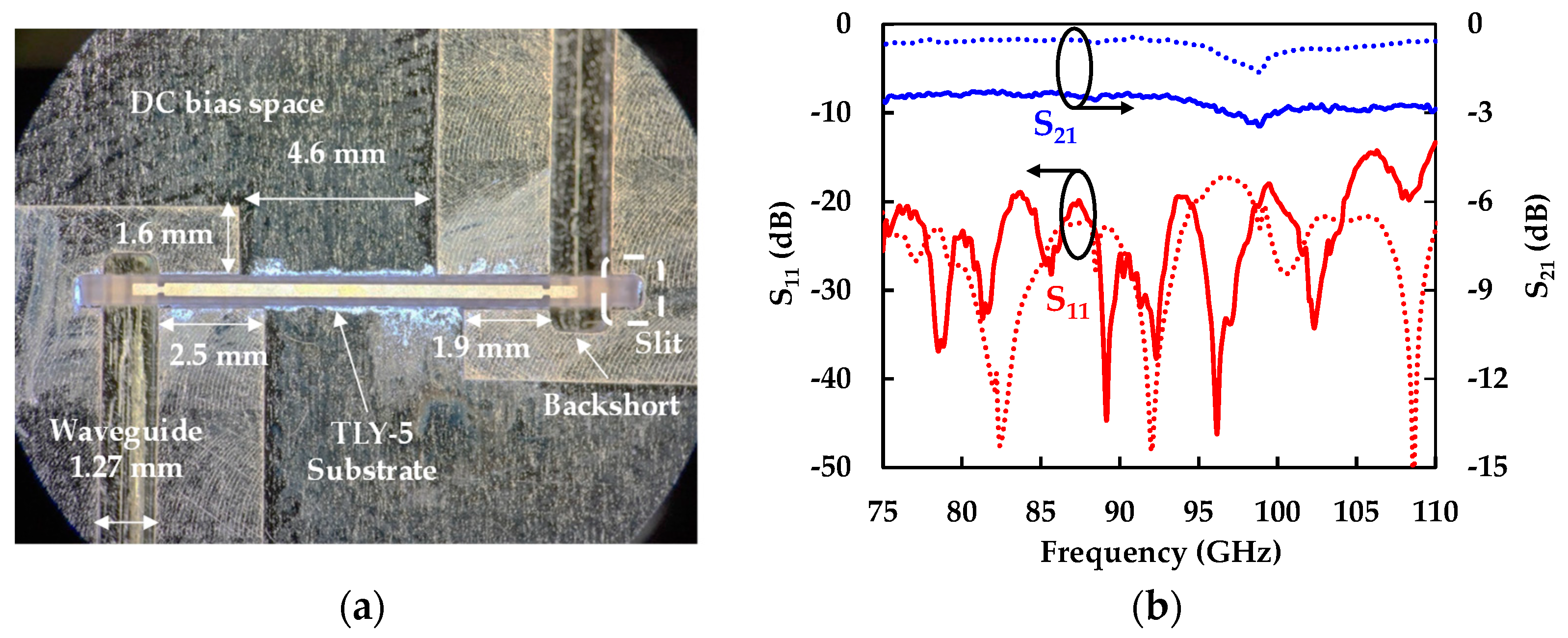
Figure 8.
Fabricated W-band transition with bond-wire and its compensation circuit. (a) Photograph. (b) Measurement results.
Figure 8.
Fabricated W-band transition with bond-wire and its compensation circuit. (a) Photograph. (b) Measurement results.

Figure 9.
Fabricated W-band LNA module: (a) External view and (b) magnified view around the LNA IC.
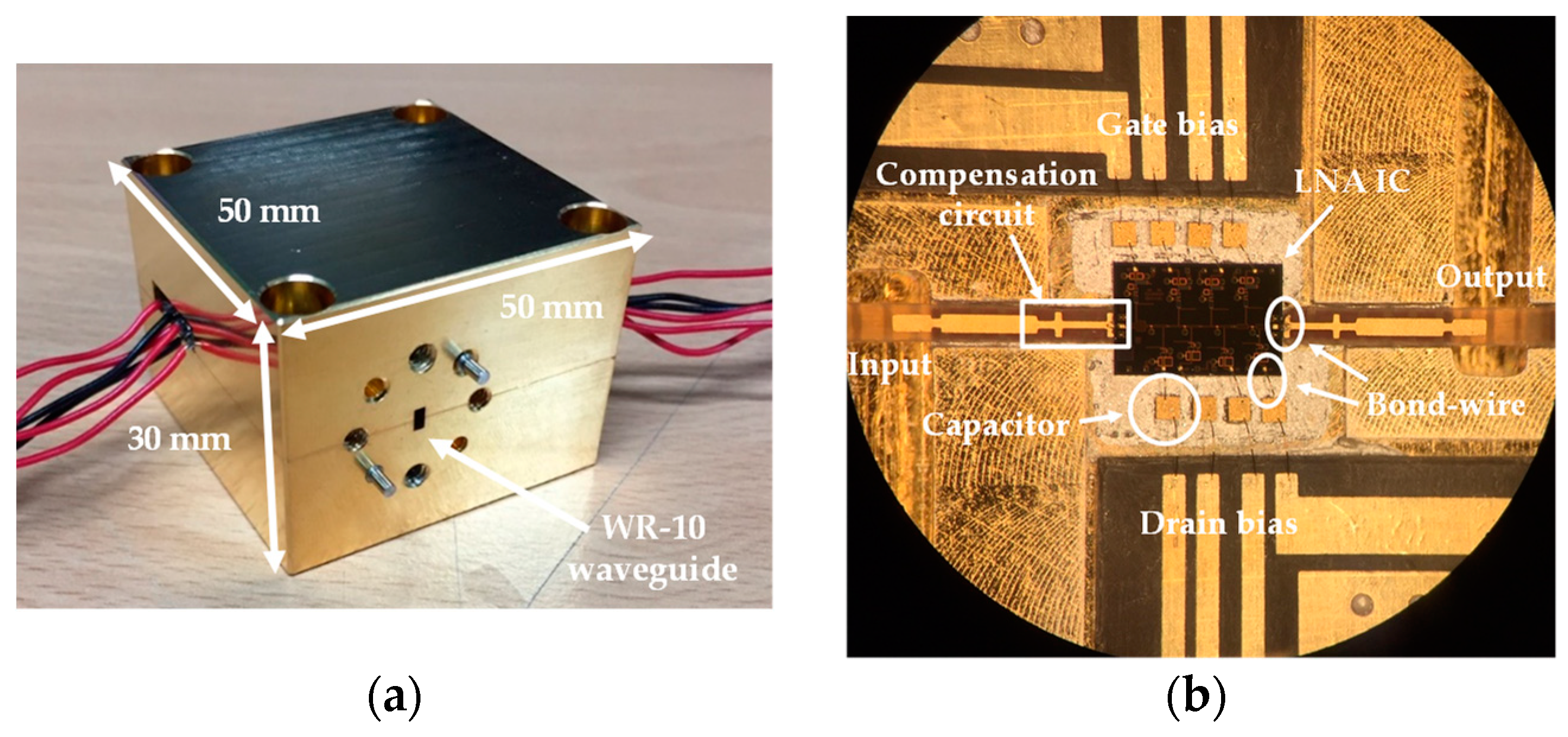
Figure 10.
Measured performance of the W-band LNA module. (a) S-parameters. (b) Noise figure.


Table 1.
Dimensions of the designed transition (in mm).
| Wp | Lp | Wm | Lm | Wc | Hc | Ws | Hs | Ds | Lbs | W50 |
|---|---|---|---|---|---|---|---|---|---|---|
| 0.3 | 0.6 | 0.15 | 0.15 | 0.8 | 0.6 | 0.8 | 0.2 | 0.7 | 0.9 | 0.32 |
© 2019 by the authors. Licensee MDPI, Basel, Switzerland. This article is an open access article distributed under the terms and conditions of the Creative Commons Attribution (CC BY) license (http://creativecommons.org/licenses/by/4.0/).
Share and Cite
MDPI and ACS Style
Doo, J.; Park, W.; Choe, W.; Jeong, J. Design of Broadband W-Band Waveguide Package and Application to Low Noise Amplifier Module. Electronics 2019, 8, 523. https://doi.org/10.3390/electronics8050523
AMA Style
Doo J, Park W, Choe W, Jeong J. Design of Broadband W-Band Waveguide Package and Application to Low Noise Amplifier Module. Electronics. 2019; 8(5):523. https://doi.org/10.3390/electronics8050523
Chicago/Turabian StyleDoo, Jihoon, Woojin Park, Wonseok Choe, and Jinho Jeong. 2019. "Design of Broadband W-Band Waveguide Package and Application to Low Noise Amplifier Module" Electronics 8, no. 5: 523. https://doi.org/10.3390/electronics8050523
Note that from the first issue of 2016, this journal uses article numbers instead of page numbers. See further details here.