Design Architectures of the CMOS Power Amplifier for 2.4 GHz ISM Band Applications: An Overview

 ,
,
Abstract
:
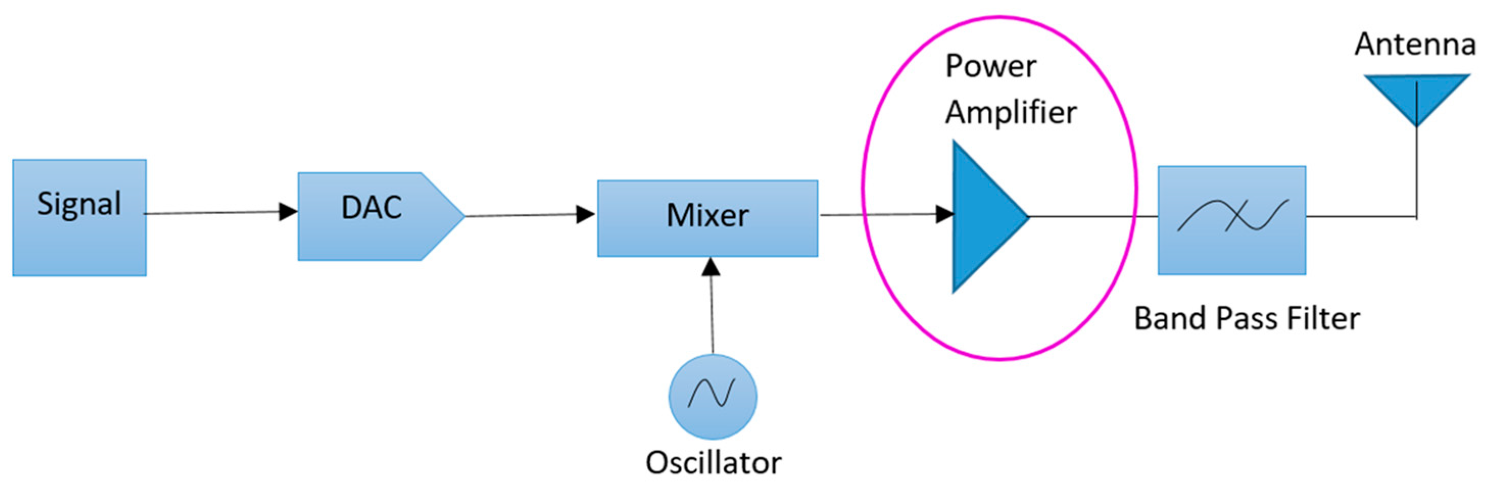
1. Introduction
2. Performance Parameters
2.1. Output Power
2.2. Power Consumption
2.3. Power Gain
2.4. Efficiency
2.5. Linearity
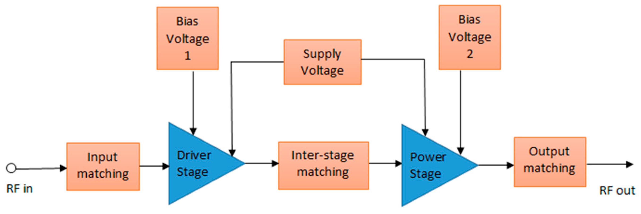
3. PA Design Classes
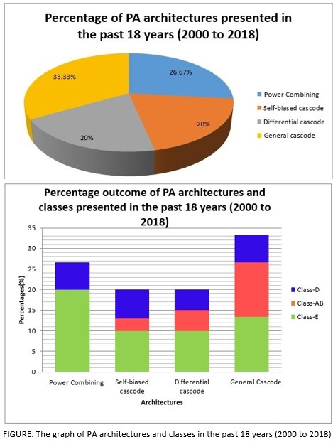
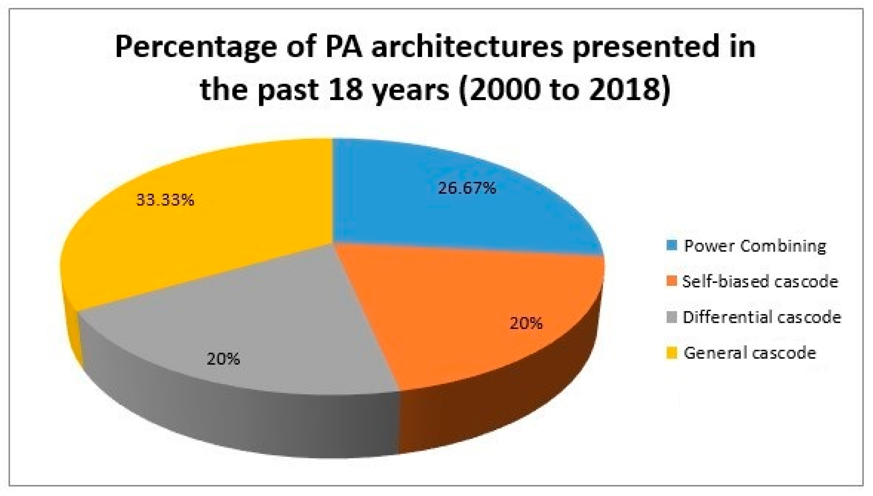
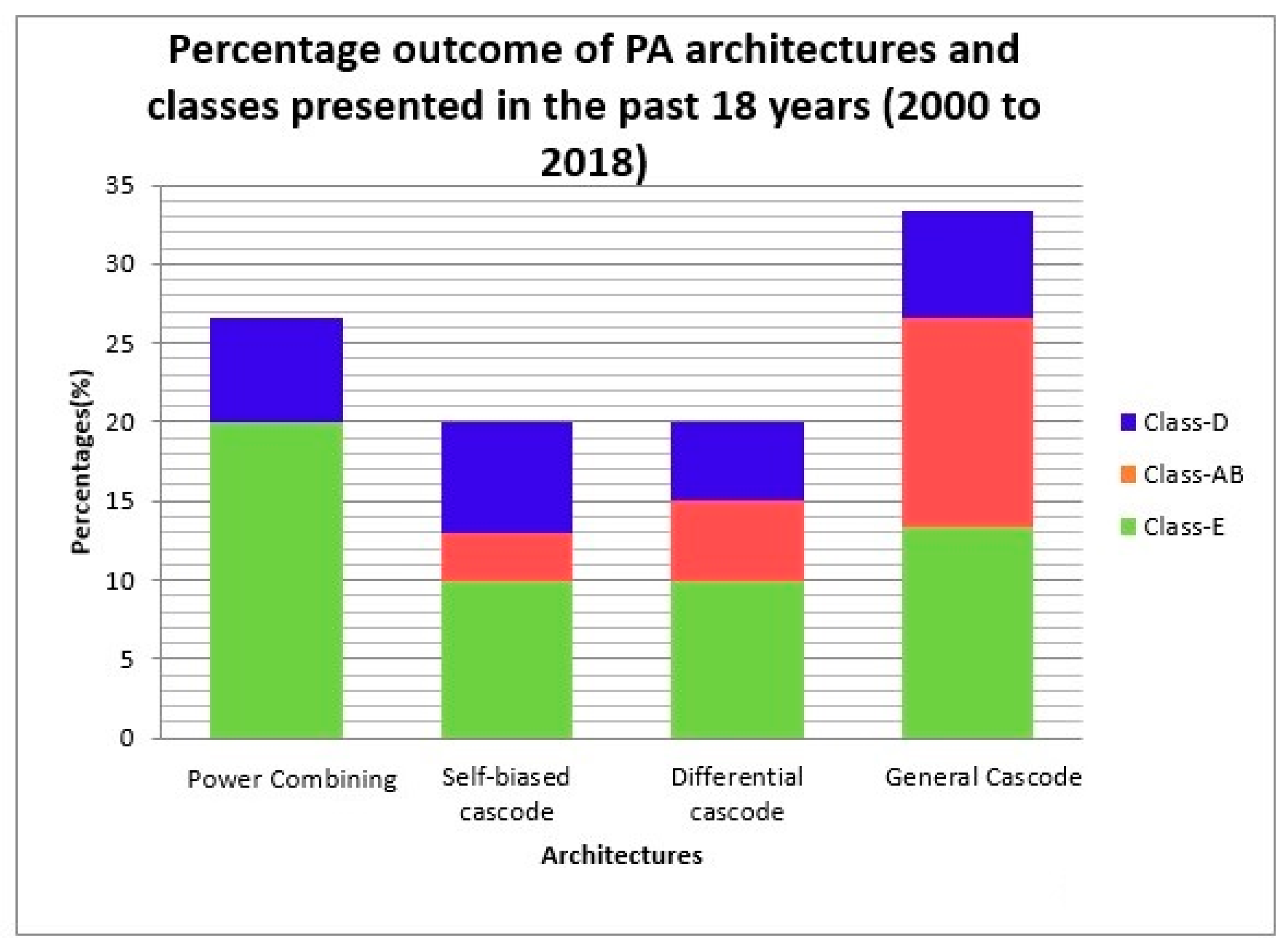
4. Advancement of 2.4 GHz CMOS PA
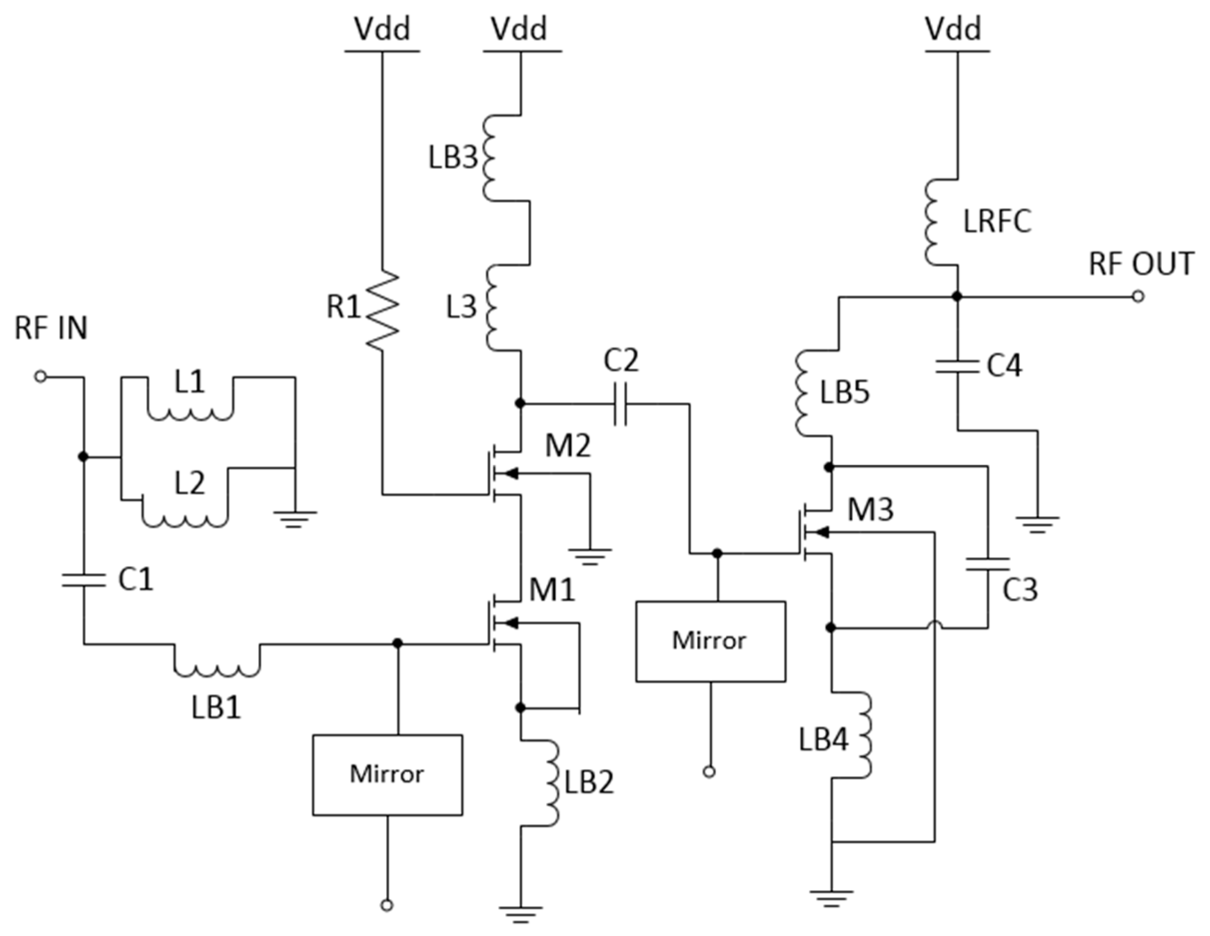
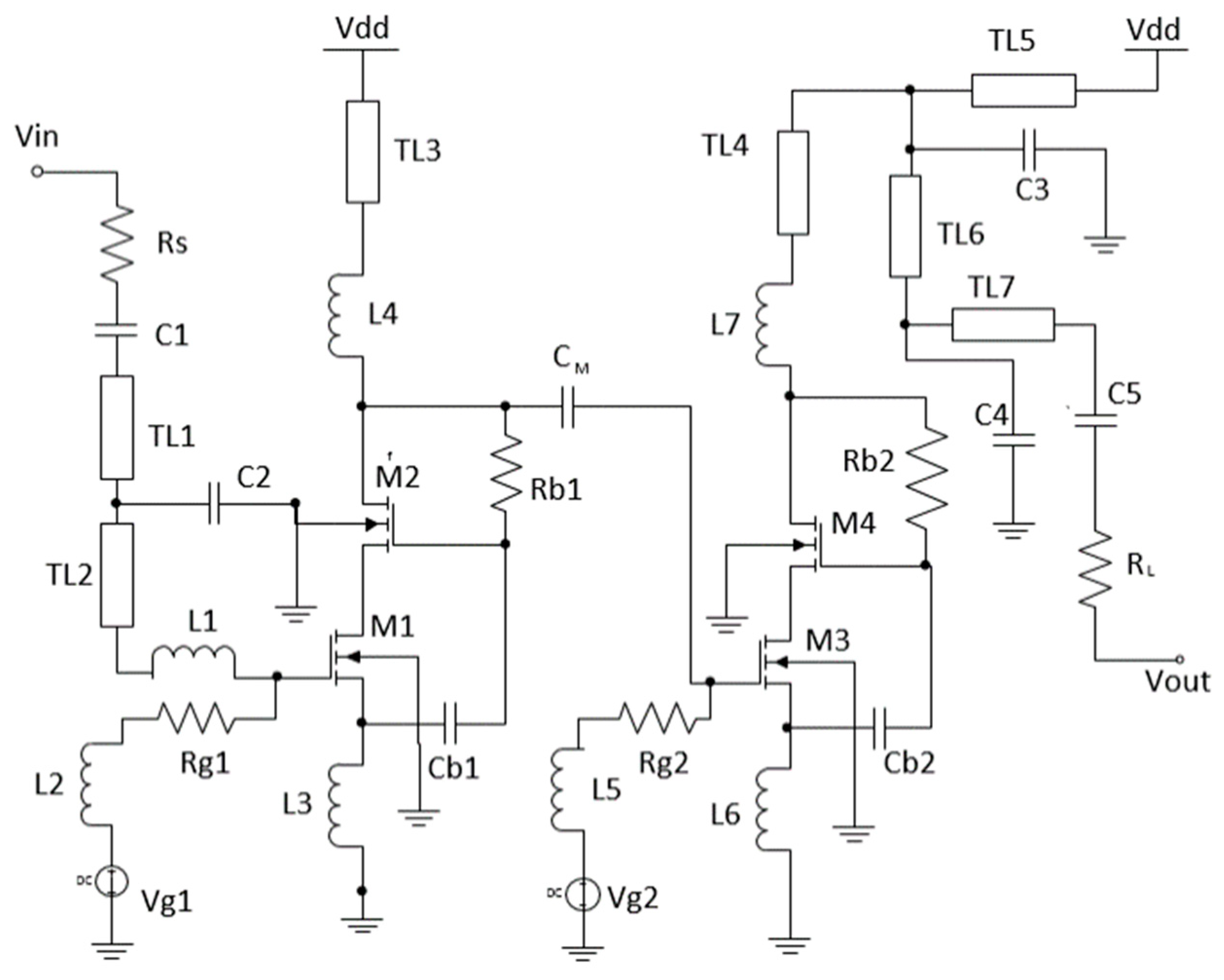
4.1. General Cascode Architecture
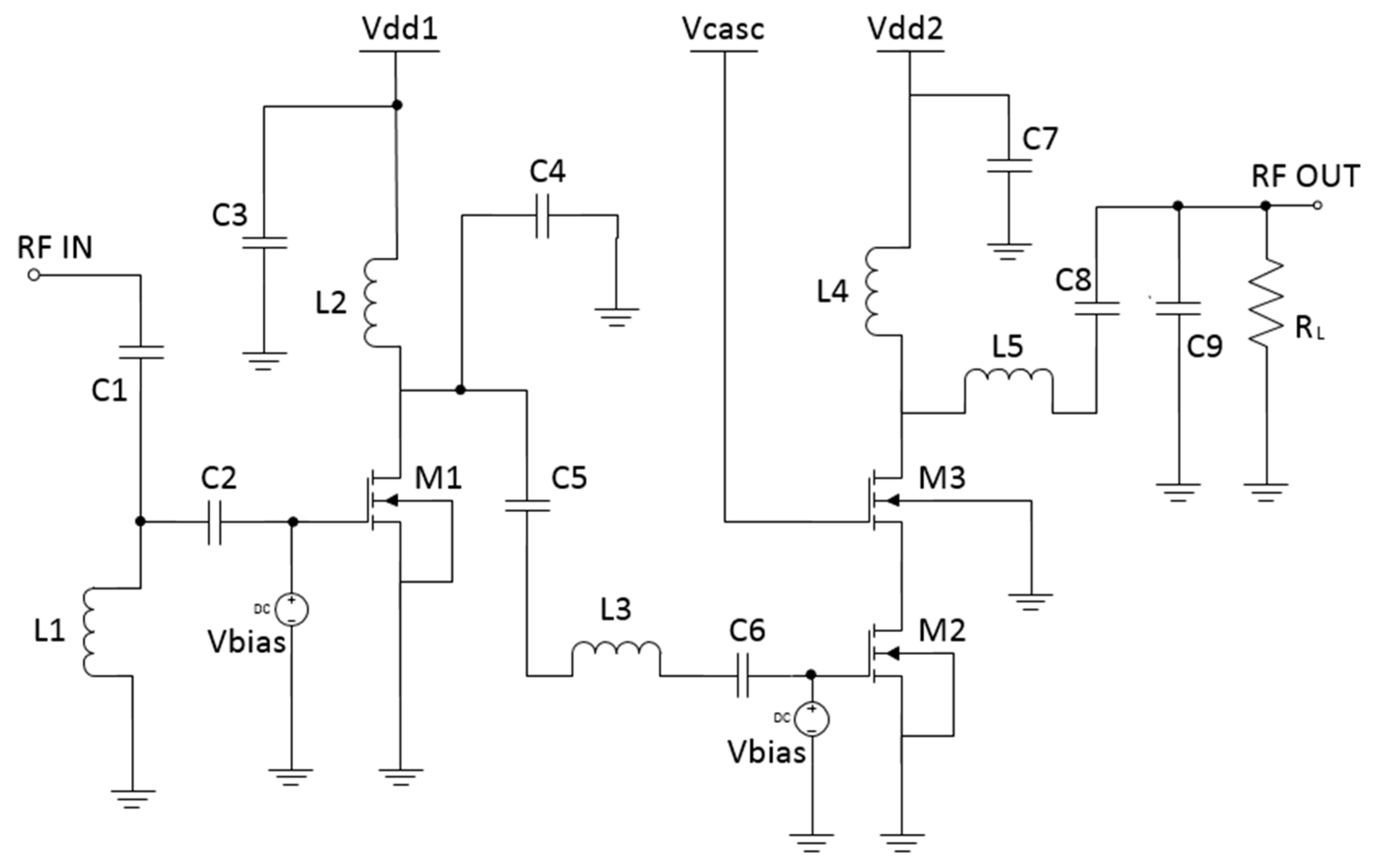
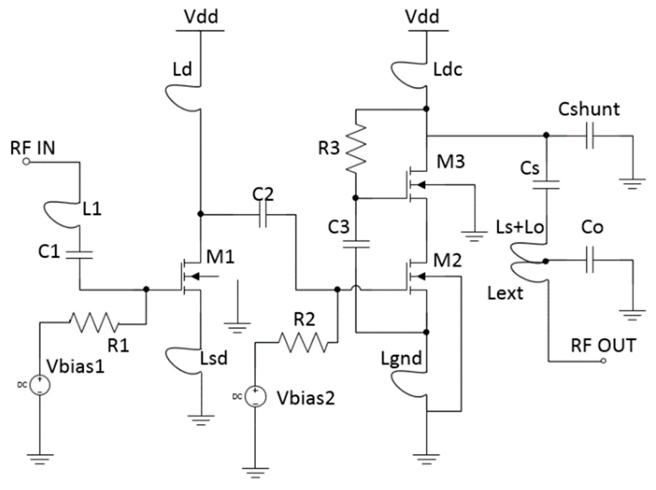
4.2. Self-Biased Cascode Architecture
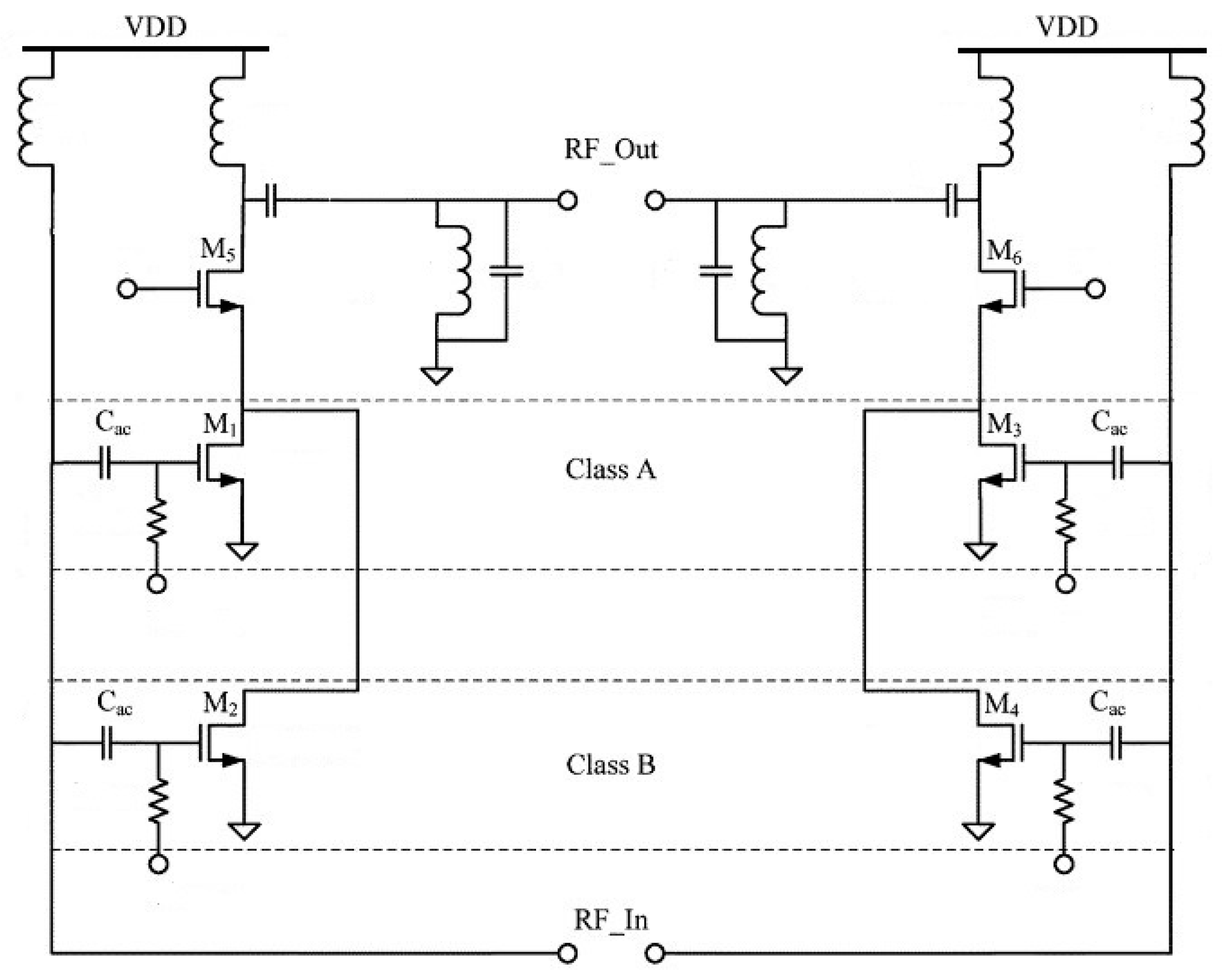
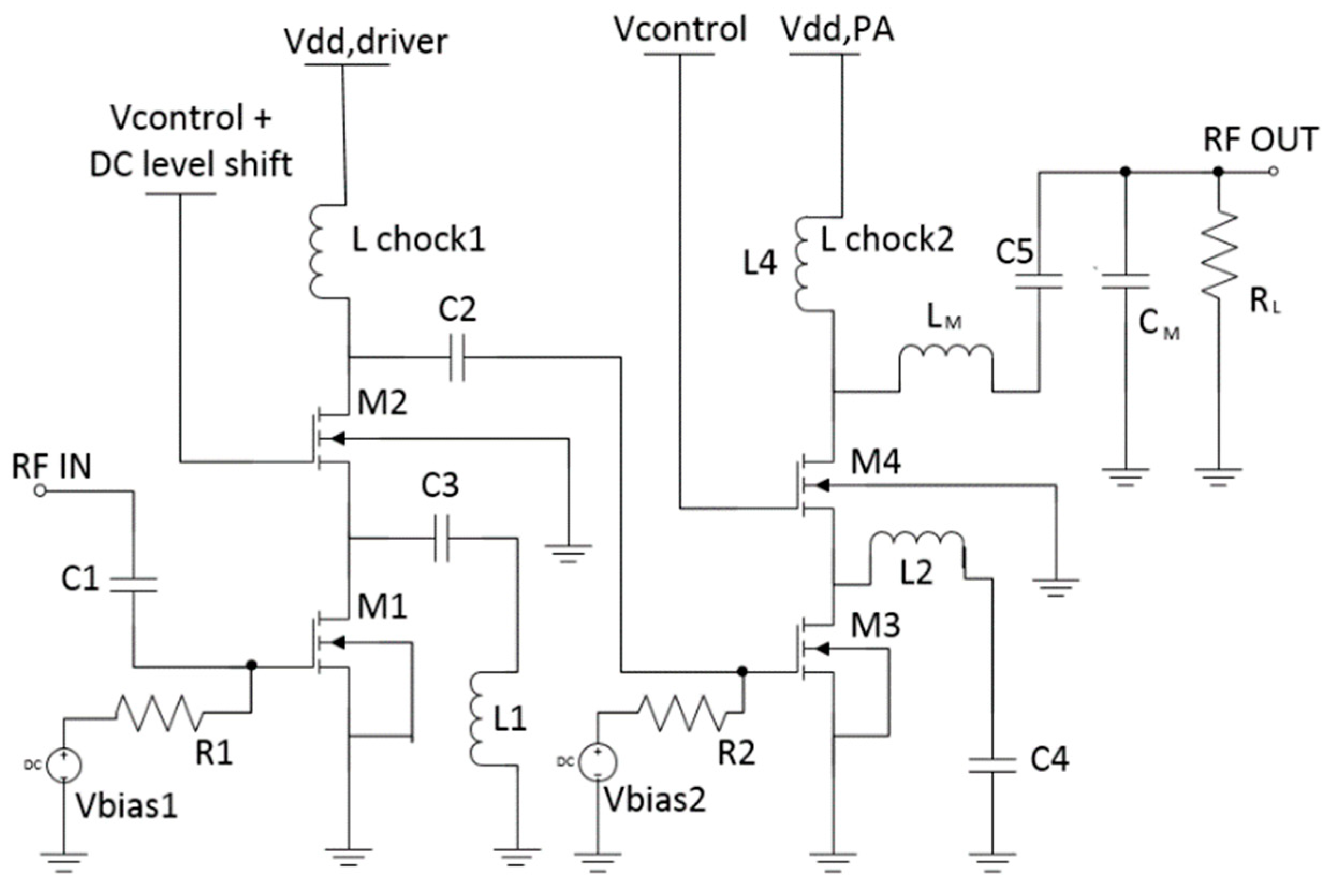
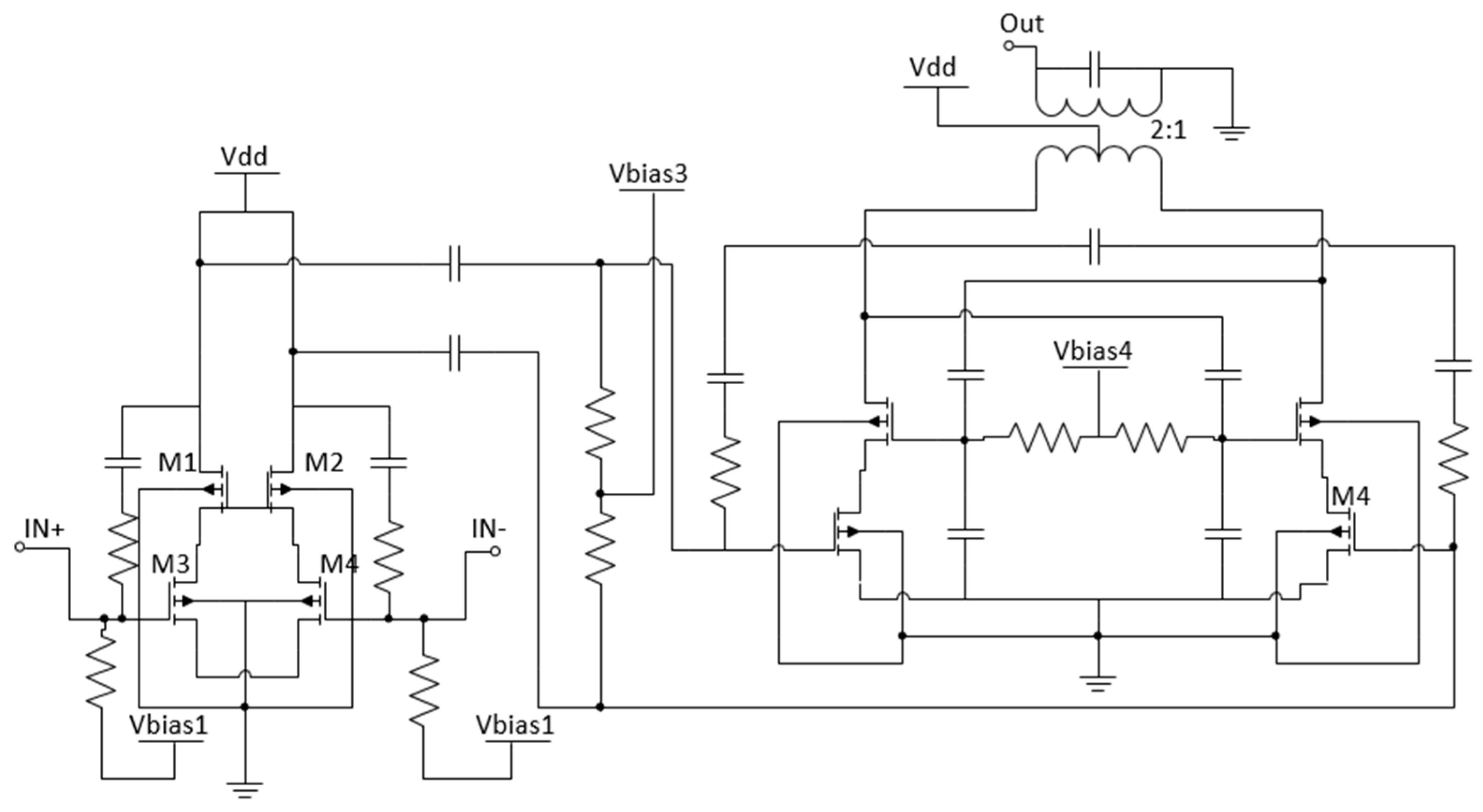
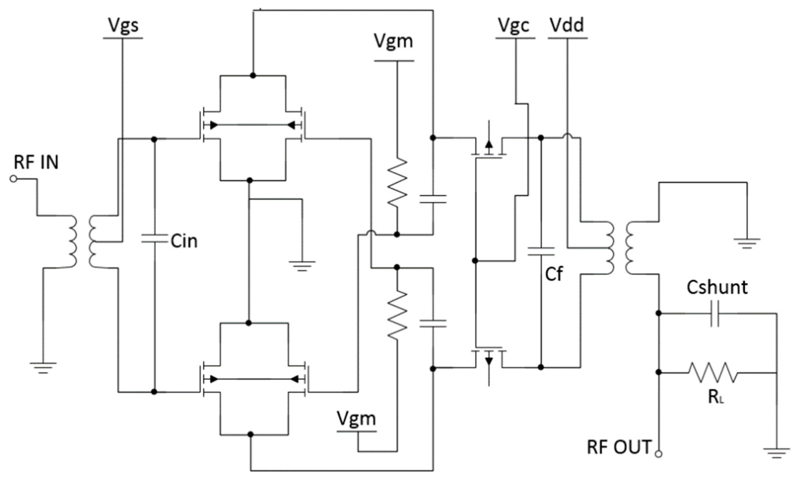
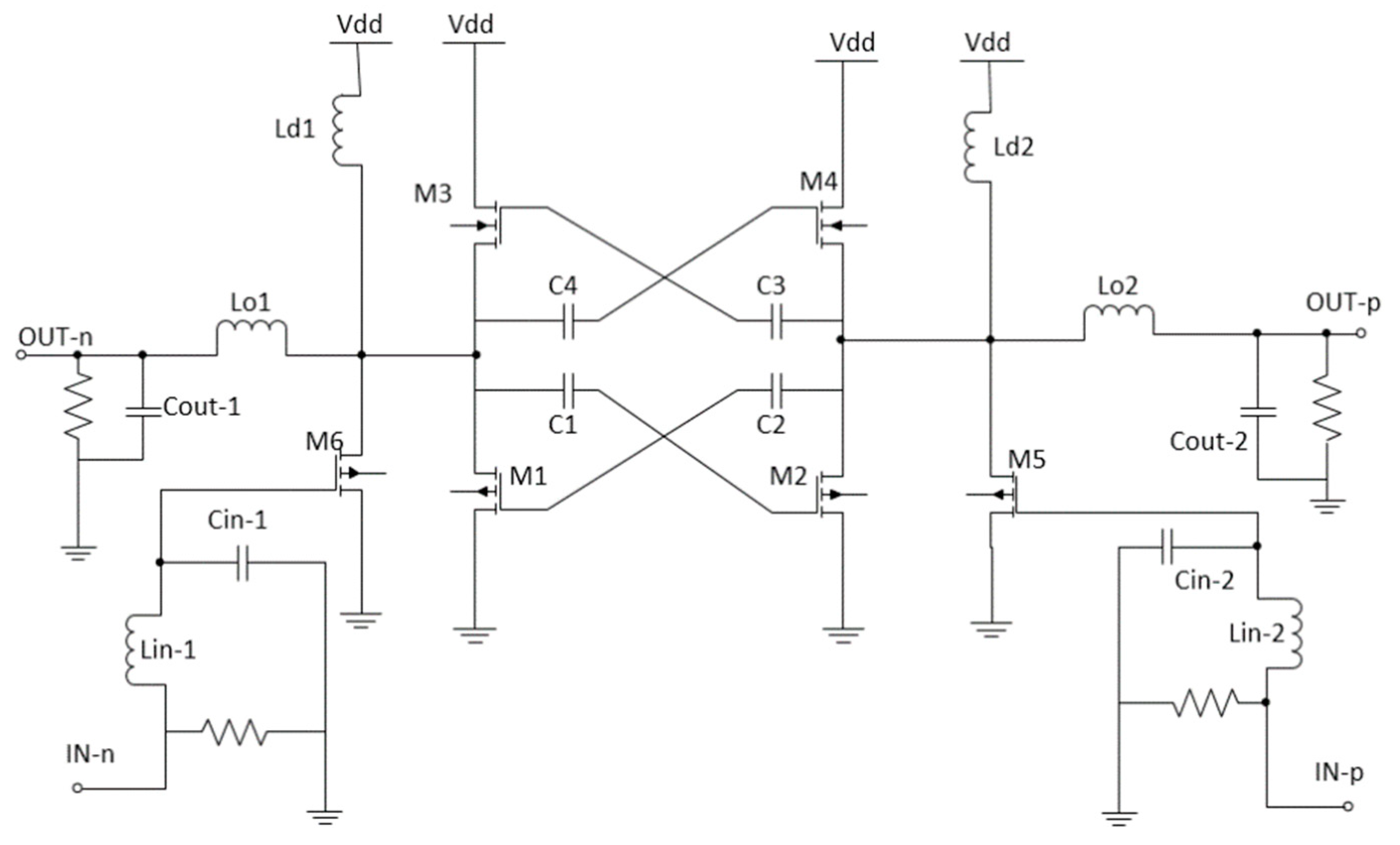
4.3. Differential Cascode Architecture
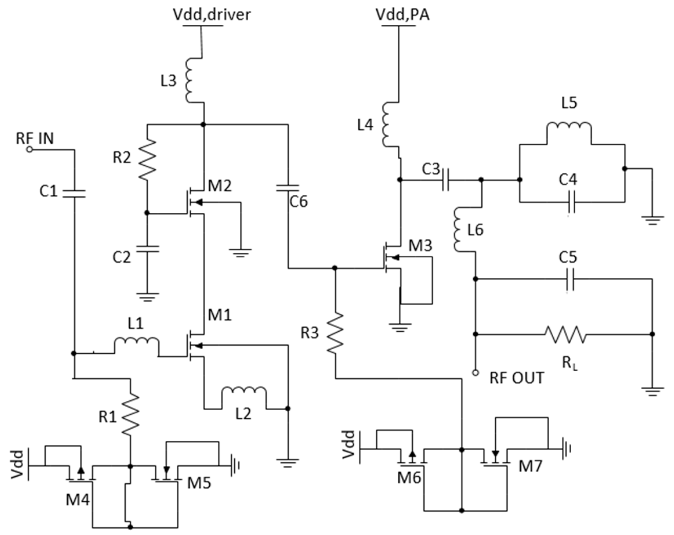
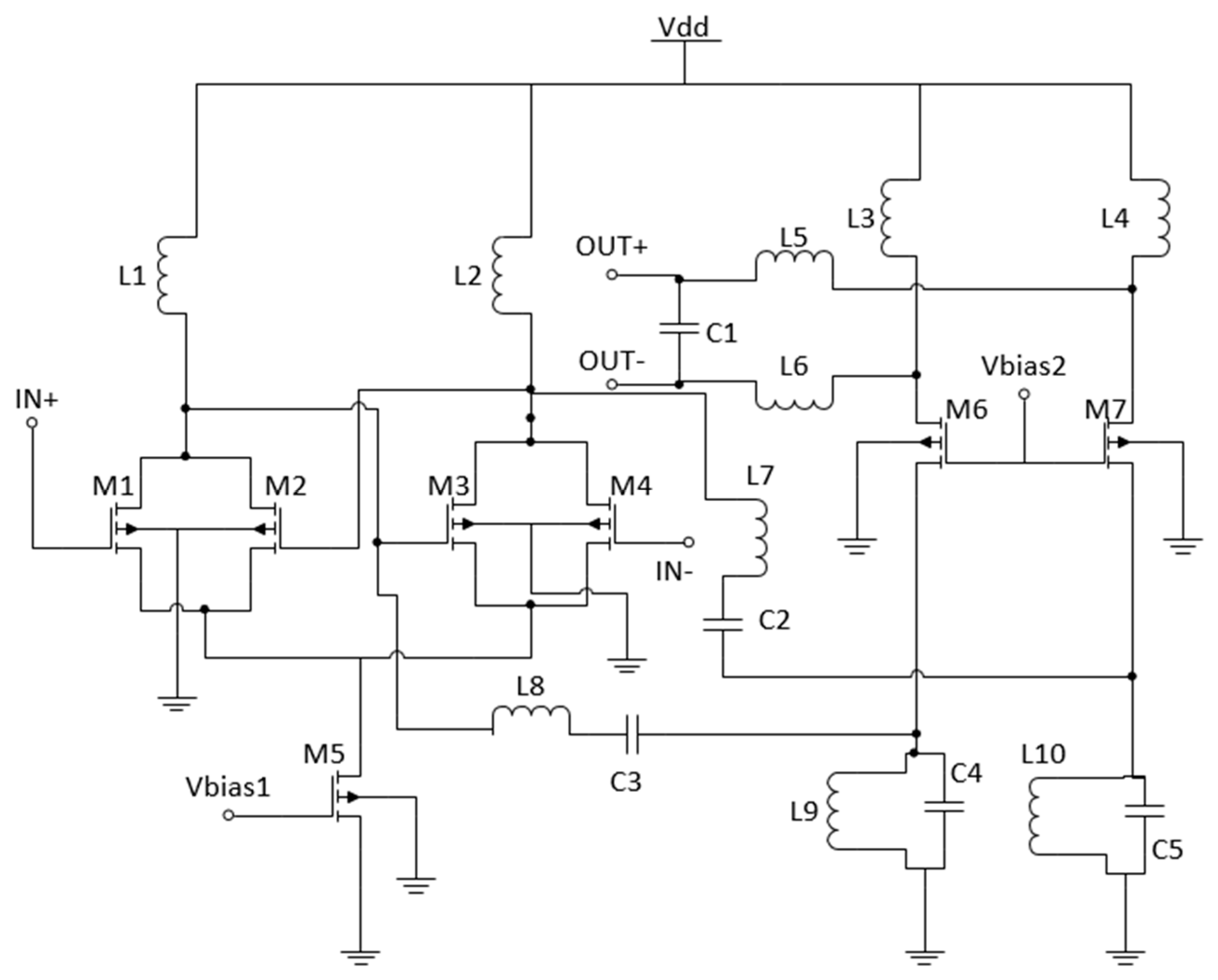
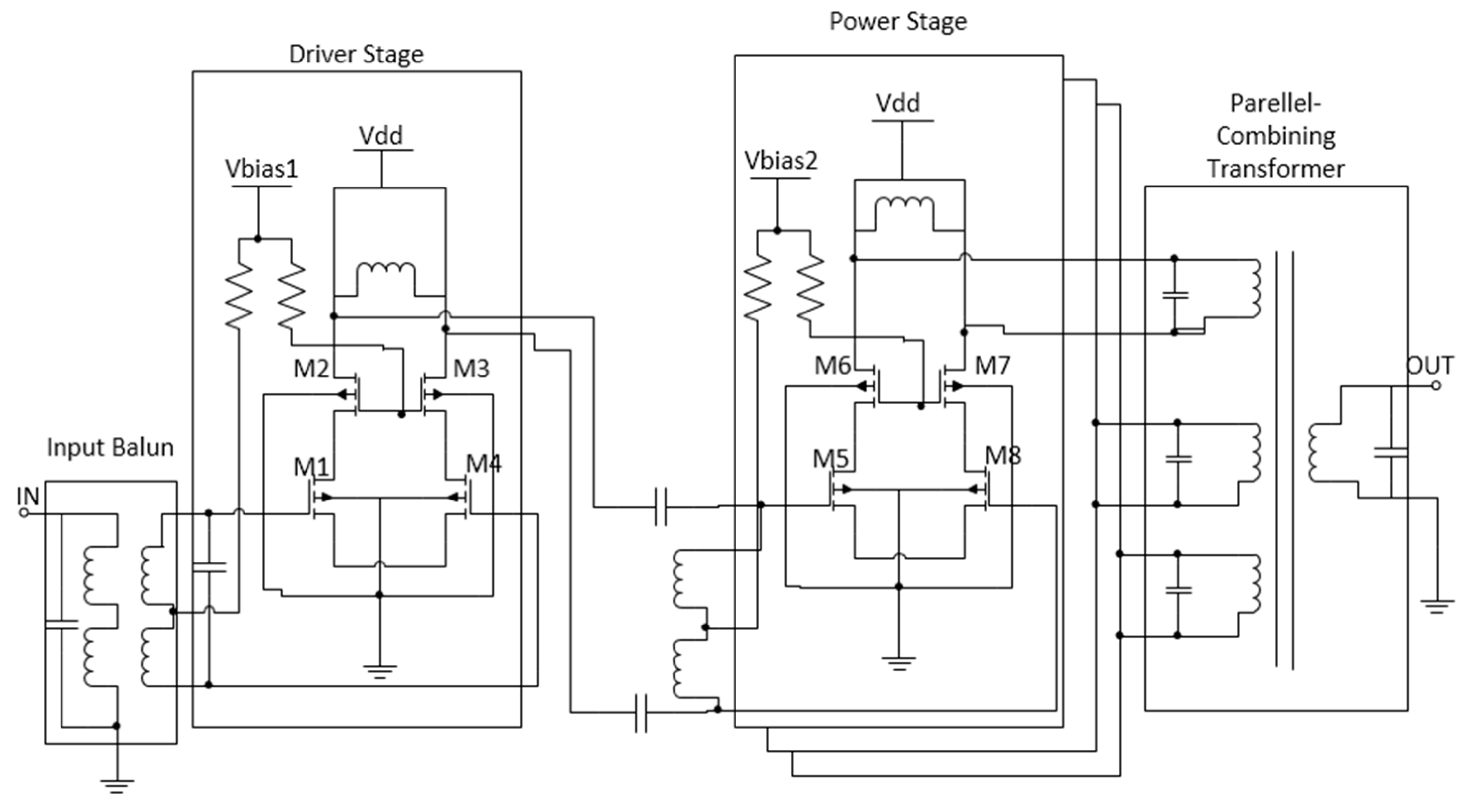
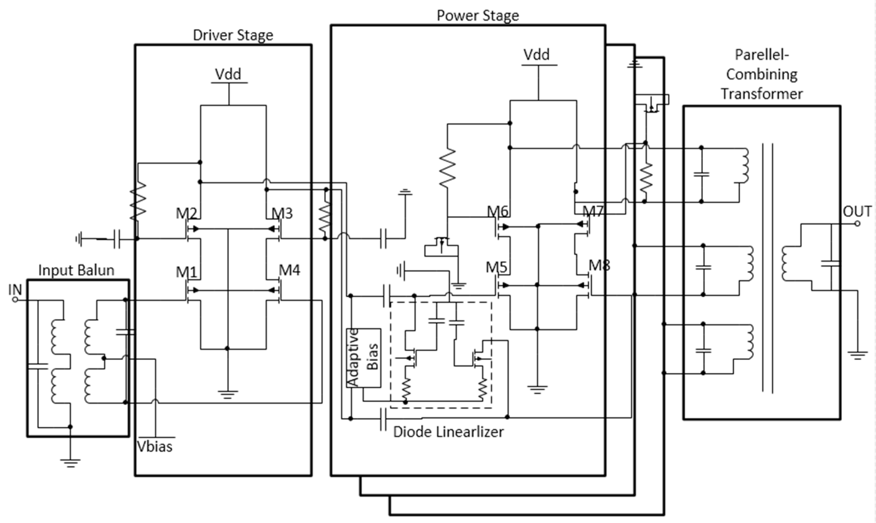
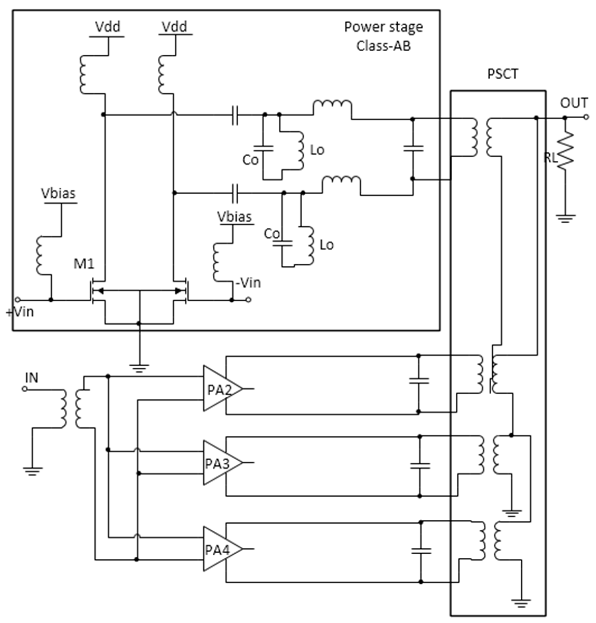
4.4. Power Combining Architecture
5. Discussion
6. Conclusions
Author Contributions
Funding
Conflicts of Interest
References
- Bhuiyan, M.; Reaz, M.; Jalil, J.; Rahman, L.; Chang, T. Design Trends in Fully Integrated 2.4 GHz CMOS SPDT Switches. Curr. Nanosci. 2014, 10, 334–343. [Google Scholar] [CrossRef]
- Ali, S.N.; Agarwal, P.; Gopal, S.; Mirabbasi, S.; Heo, D. A 25–35 GHz Neutralized Continuous Class-F CMOS Power Amplifier for 5G Mobile Communications Achieving 26% Modulation PAE at 1.5 Gb/s and 46.4% Peak PAE. IEEE Trans. Circuits Syst. I Regul. Pap. 2019, 66, 834–847. [Google Scholar] [CrossRef]
- Badal, T.I.; Reaz, M.B.I.; Bhuiyan, M.A.S.; Kamal, N. CMOS Transmitters for 2.4-GHz RF Devices: Design Architectures of the 2.4-GHz CMOS Transmitter for RF Devices. IEEE Microw. Mag. 2019, 20, 38–61. [Google Scholar] [CrossRef]
- Bhuiyan, M.A.S.; Chew, J.X.; Reaz, M.B.I.; .Kamal, N. Design of an active inductor based LNA in Silterra 130 nm CMOS process technology. Inf. Midem 2015, 45, 188–194. [Google Scholar]
- Bhuiyan, M.A.; Zijie, Y.; Yu, J.S.; Reaz, M.B.; Kamal, N.; Chang, T.G. Active inductor based fully integrated CMOS transmit/receive switch for 2.4 GHz RF transceiver. Anais da Academia Brasileira de Ciências 2016, 88, 1089–1098. [Google Scholar] [CrossRef]
- Badal, M.T.I.; Reaz, M.B.I.; Jalil, Z.; Bhuiyan, M.A.S. Low Power High-Efficiency Shift Register Using Implicit Pulse-Triggered Flip-Flop in 130 nm CMOS Process for a Cryptographic RFID Tag. Electronics 2016, 5, 92. [Google Scholar] [CrossRef]
- Schmiedeke, P.; Bhuiyan, M.A.S.; Reaz, M.B.I.; Chang, T.G.; Crespo, M.L.; Cicuttin, A. A fully integrated high IP1dB CMOS SPDT switch using stacked transistors for 2.4 GHz TDD transceiver applications. Sadhana 2018, 43, 94. [Google Scholar] [CrossRef]
- Issa, A.H.; Ghayyib, S.M.; Ezzulddin, A.S. Toward a fully integrated 2.4GHz differential pair class-E power amplifier using on-chip RF power transformers for Bluetooth systems. AEU Int. J. Electron. Commun. 2015, 69, 182–187. [Google Scholar] [CrossRef]
- Kamerman, A.; Monteban, L.; Zysman, G.I. WaveLAN®-II: A high-performance wireless LAN for the unlicensed band. Bell Labs Tech. J. 2002, 2, 118–133. [Google Scholar] [CrossRef]
- Kumar, R.; Kumar, M.; Balrajb, M. Design and Implementation of a High Efficiency CMOS Power Amplifier for Wireless Communication at 2.45 GHz. In Proceedings of the 2012 International Conference on Communication Systems and Network Technologies (CSNT 2012), Gujarat, India, 11–13 May 2012; pp. 804–807. [Google Scholar]
- Rostomyan, N.; Özen, M.; Asbeck, P. 28 GHz Doherty Power Amplifier in CMOS SOI With 28% Back-Off PAE. IEEE Microw. Wirel. Compon. Lett. 2018, 28, 446–448. [Google Scholar] [CrossRef]
- Wu, H.; Li, B.; Hu, Y.; Wang, K.; Liang, Z.; Wu, Z.; Liu, Y. Fully-integrated linear CMOS power amplifier with proportional series combining transformer for S-Band applications. IEICE Electron. 2018, 15, 20171100. [Google Scholar] [CrossRef]
- Roy, P.; Dawn, D. Fully integrated CMOS power amplifier using resistive current combining technique. IET Microwav. Anten. Propag. 2018, 12, 826–832. [Google Scholar] [CrossRef]
- Kim, J. Linear CMOS power amplifier using continuous gate voltage control. Microw. Opt. Technol. Lett. 2018, 60, 337–341. [Google Scholar] [CrossRef]
- Kim, K.; Ko, J.; Nam, S.; Lee, S. A Two-Stage Broadband Fully Integrated CMOS Linear Power Amplifier for LTE Applications. IEEE Trans. Circuits Syst. II Briefs 2016, 63, 533–537. [Google Scholar] [CrossRef]
- Bameri, H.; Hakimi, A.; Movahhedi, M. A linear-high range output power control technique for cascode power amplifiers. Microelectron. J. 2011, 42, 1025–1031. [Google Scholar] [CrossRef]
- Sowlati, T.; Leenaerts, D. A 2.4-ghz 0.18-μm cmos self-biased cascode power amplifier. IEEE J. Circuits 2003, 38, 1318–1324. [Google Scholar] [CrossRef]
- Bhuiyan, M.A.S.; Reaz, M.B.I.; Jalil, J.; Rahman, L.F. Design of a nanoswitch in 130 nm CMOS technology for 2.4 GHz wireless terminals. Bull. Pol. Acad. Sci. Tech. Sci. 2014, 62, 399–406. [Google Scholar] [CrossRef] [Green Version]
- Van Praet, C.; Spiessens, P.; Tubbax, H.; Stubbe, F.; Li, Z.; Torfs, G.; Bauwelinck, J.; Yin, X.; Vandewege, J. A 2.45-GHz +20-dBm fast switching class-E power amplifier with 43% PAE and an 18-dB-wide power range in 0.18-um CMOS. IEEE Trans. Circuits Syst. II Briefs 2012, 59, 224–228. [Google Scholar] [CrossRef]
- Sahu, S.R.; Deshmukh, A.Y. Design of High Efficiency Two Stage Power Amplifier in 0.13 µM RF CMOS Technology for 2.4GHZ WLAN Application. Int. J. VLSI Des. Commun. Syst. 2013, 4, 31–40. [Google Scholar] [CrossRef]
- Santana, D.B.; Klimach, H.; Fabris, E.; Bampi, S. CMOS RF class-E power amplifier with power control. In Proceedings of the 2016 IEEE 7th Latin American Symposium on Circuits & Systems (LASCAS), Florianopolis, Brazil, 28 February–2 March 2016; pp. 371–374. [Google Scholar] [CrossRef]
- Yen, C.-C.; Chuang, H.-R. A 0.25-μm 20-dBm 2.4-GHz CMOS power amplifier with an integrated diode linearizer. IEEE Microw. Wirel. Compon. Lett. 2003, 13, 45–47. [Google Scholar] [CrossRef]
- Zhang, X.; Yan, J.; Shi, Y.; Dai, F.F. A 2.4GHz Power Amplifier Driver used in a WLAN IEEE 802.11b/g Transmitter Front-End. In Proceedings of the 2008 4th IEEE International Conference on Circuits and Systems for Communications (ICCSC 2008), Shanghai, China, 26–28 May 2008; pp. 55–59. [Google Scholar] [CrossRef]
- Fritzin, J. Power Amplifier Circuits in CMOS Technologies. Ph.D. Thesis, Linköping University, Linköping, Sweden, 2009. [Google Scholar]
- An, K.H. CMOS RF Power Amplifiers for Mobile Wireless Communications. Ph.D. Thesis, Georgia Institute of Technology, Atlanta, GA, USA, 2009. [Google Scholar]
- Sarwar, A. CMOS power Consumption and CPD Calculation; Texas Instruments Incorporated: Dallas, TX, USA, 1997. [Google Scholar]
- Lee, O. High Efficiency Switching CMOS Power Amplifiers for Wireless Communications. Ph.D. Thesis, Georgia Institute of Technology, Atlanta, GA, USA, 2009. [Google Scholar]
- Choi, H.; Jung, H.; Shung, K.K. Power Amplifier Linearizer for High Frequency Medical Ultrasound Applications. J. Med. Boil. Eng. 2015, 35, 226–235. [Google Scholar] [CrossRef] [Green Version]
- Sokal, N.O. RF power amplifiers, classes A through S-how they operate, and when to use each. In Proceedings of the IEEE Professional Program Proceedings. Electronic Industries Forum of New England, Boston, MA, USA, 6–8 May 1997; pp. 179–252. [Google Scholar] [CrossRef]
- Samal, L.; Mahapatra, K.K.; Raghuramaiah, K. Class-C power amplifier design for GSM application. In Proceedings of the 2012 International Conference on Computing, Communication and Applications, Tamilnadu, India, 22–24 February 2012; pp. 1–5. [Google Scholar] [CrossRef]
- Cai, W.; Huang, L.; Wang, S. Class D Power Amplifier for Medical Application. Inf. Eng. Int. J. 2016, 4, 9–15. [Google Scholar] [CrossRef]
- Ma, L.; Zhou, J.; Yu, Z. Design of a class-F power amplifier with expanding bandwidth. In Proceedings of the 2015 Asia-Pacific Microwave Conference (APMC), Nanjing, China, 6–9 December 2015; pp. 1–3. [Google Scholar] [CrossRef]
- Ding, Y.; Harjani, R. A high-efficiency CMOS +22-dBm linear power amplifier. IEEE J. Circuits 2005, 40, 1895–1900. [Google Scholar] [CrossRef]
- Saari, V.; Juurakko, P.; Ryynänen, J.; Halonen, K. Integrated 2.4 GHz class-E CMOS power amplifier. In Proceedings of the IEEE Radio Frequency Integrated Circuits Symposium, Long Beach, CA, USA, 12–14 June 2005; pp. 645–648. [Google Scholar] [CrossRef]
- Sira, D.; Thomsen, P.; Larsen, T. A cascode modulated class-E power amplifier for wireless communications. Microelectron. J. 2011, 42, 141–147. [Google Scholar] [CrossRef]
- Fouad, H.; Zekry, A.H.; Fawzy, K. Self-Biased 0.13 µm CMOS 2.4-GHz Class E Cascode Power Amplifier. In Proceedings of the 26th National Radio Science Conference, New Cairo, Egypt, 17–19 March 2009; pp. 1–12. [Google Scholar]
- Murad, S.A.Z.; Pokharel, R.K.; Kanaya, H.; Yoshida, K.; Nizhnik, O. A 2.4-GHz 0.18-μm CMOS Class E single-ended switching power amplifier with a self-biased cascode. AEU Int. J. Electron. Commun. 2010, 64, 813–818. [Google Scholar] [CrossRef]
- Hong, J.; Imanishi, D.; Okada, K.; Matsuzawa, A. A 2.4 GHz fully integrated CMOS power amplifier using capacitive cross-coupling. In Proceedings of the 2010 IEEE International Conference on Wireless Information Technology and Systems, Honolulu, HI, USA, 28 August–3 September 2010; pp. 1–4. [Google Scholar] [CrossRef]
- Luo, S.; Potomac, M. Simple Self-Biased Cascode Amplifier Circuit. U.S. Patent Application Publication US20040085130A1, 6 May 2004. [Google Scholar]
- Kiumarsi, H.; Mizuochi, Y.; Ito, H.; Ishihara, N.; Masu, K. A Three-Stage Inverter-Based Stacked Power Amplifier in 65 nm Complementary Metal Oxide Semiconductor Process. Jpn. J. Appl. Phys. 2012, 51, 2. [Google Scholar] [CrossRef]
- Ho, K.-W.; Luong, H.C. A 1-V CMOS power amplifier for bluetooth applications. IEEE Trans. Circuits Syst. II Briefs 2003, 50, 445–449. [Google Scholar] [CrossRef]
- Lee, C.; Park, C. 2.4 GHz CMOS Power Amplifier with Mode-Locking Structure to Enhance Gain. Sci. J. 2014, 2014, 5–10. [Google Scholar] [CrossRef]
- Ghorbani, A.R.; Ghaznavi-Ghoushchi, M.B. A 35.6dB, 43.3% PAE class E differential power amplifier in 2.4GHz with cross coupling neutralization for IoT applications. In Proceedings of the 24th Iranian Conference on Electrical Engineering (ICEE), Shiraz, Iran, 10–12 May 2016; pp. 490–495. [Google Scholar] [CrossRef]
- Zhuo, W.; Li, X.; Shekhar, S.; Embabi, S.; De Gyvez, J.; Allstot, D.; Sanchez-Sinencio, E. A capacitor cross-coupled common-gate low-noise amplifier. IEEE Trans. Circuits Syst. II Briefs 2005, 52, 875–879. [Google Scholar] [CrossRef] [Green Version]
- Asada, H.; Matsushita, K.; Bunsen, K.; Okada, K.; Matsuzawa, A. A 60GHz CMOS power amplifier using capacitive cross-coupling neutralization with 16% PAE. In Proceedings of the 41st European Microwave Conference (EuMC 2011), Manchester, UK, 10–13 October 2011; pp. 1115–1118. [Google Scholar]
- An, K.H.; Lee, D.H.; Lee, O.; Kim, H.; Han, J.; Kim, W.; Lee, C.-H.; Kim, H.; Laskar, J. A 2.4 GHz Fully Integrated Linear CMOS Power Amplifier With Discrete Power Control. IEEE Microw. Wirel. Compon. Lett. 2009, 19, 479–481. [Google Scholar] [CrossRef]
- Lee, T.H. The Design of CMOS Radio-Frequency Integrated Circuits, 2nd ed.; Cambridge University Press (CUP): Cambridge, UK, 2003. [Google Scholar]
- Ren, Z.; Zhang, K.; Liu, L.; Li, C.; Chen, X.; Liu, D.; Liu, Z.; Zou, X. On-chip power-combining techniques for watt-level linear power amplifiers in 0.18 μm CMOS. J. Semicond. 2015, 36, 95002. [Google Scholar] [CrossRef]
- An, K.H.; Lee, O.; Kim, H.; Lee, D.H.; Han, J.; Yang, K.S.; Kim, Y.; Chang, J.J.; Woo, W.; Lee, C.-H.; et al. Power-Combining Transformer Techniques for Fully-Integrated CMOS Power Amplifiers. IEEE J. Circuits 2008, 43, 1064–1075. [Google Scholar] [CrossRef]
- Ezzulddin, A.S.; Jasim, S.H. Design of RF Power Amplifiers using Parallel-Series Power Combining Transformers. Eng. Technol. J. 2015, 33, 294–307. [Google Scholar]
- Mazzanti, A.; Larcher, L.; Brama, R. Analysis of reliability and power efficiency in cascode class-E Pas. IEEE J. Solid-State Circ. 2006, 41, 1222–1229. [Google Scholar] [CrossRef]
- Mandal, P.; Viisvanathan, V. A Self-Biased High Performance Folded Cascode CMOS Op-Amp. In Proceedings of the 10th International Conference on VLSI Design, Hyderabad, India, 4–7 January 1997; pp. 429–434. [Google Scholar] [CrossRef]
- Tsai, K.C.; Gray, P.R. A 1.9GHz 1W CMOS Class-E Power Amplifier for Wireless Communications. IEEE J. Solid-State Circ. 1999, 34, 962–970. [Google Scholar] [CrossRef]
- Baek, S.; Ryu, H.; Nam, I.; Jeong, M.; Kim, B.; Lee, O. A 2.4-GHz CMOS Power Amplifier with Parallel-Combined Transistors and Selective Adaptive Biasing for Wireless Lan Applications. Microw. Opt. Technol. Lett. 2016, 58, 1374–1377. [Google Scholar] [CrossRef]
- Yoo, J.; Lee, C.; Kang, I.; Son, M.; Sim, Y.; Park, C. 2.4-GHz CMOS Linear Power Amplifier for IEEE 802.11N WLAN Applications. Microw. Opt. Technol. Lett. 2017, 59, 546–550. [Google Scholar] [CrossRef]


| Architectures | Design Techniques of Architectures | Advantages | Disadvantages |
|---|---|---|---|
| General Cascode | - The source terminal of the transistor is connected to cascode with the drain of another transistor - The gate of transistors is biased with DC voltages. | - Eliminates oxide breakdown and hot carrier effect - Circuit simplicity - Low power consumption - High power gain and PAE - Small chip size | - Additional power losses in CG transistor - Moderate output power |
| Self-Biased Cascode | - A resistor and a capacitor produce bias for the transistor to reduce the extra DC voltage supply needed - Allow RF signal swing at the common gate of two cascaded transistors to improve the biasing voltage. | - No external bias supplies needed - Can overcome the device stress - Simpler circuit and low-cost circuit - High power gain - Reduced power consumption | - Required high supply voltage - Low slew rate with slow react time of PA to the input level - The supply voltage is limited by the breakdown voltage of CG |
| Differential Cascode | - Cross-coupling capacitors are used to decrease the power dissipation of PA with increasing transconductance. - The cross-coupling transistors form a positive feedback on driver stage is used to obtain a high efficiency | - Minimized common mode noise and substrate coupling - Minimized impedance matching losses - No low breakdown voltage problem | - Considerably less PAE - More complex circuitry - Average output power |
| Power Combining Architecture | - Three identical PAs are combined in parallel to form a transformer - LC balun is used as the input balun for an effective input matching. | - Reduction of secondary inductor losses - Generate high output power - High power gain | - Large chip size and high cost - Complex circuitry - High power consumption - Poor PAE performance |
| Reference (Year) | CMOS Technology (µm) | Supply Voltage (V) | Architectures | Classes | Power Consumed (W) | Power Gain (dB) | PAE (%) | Output Power (dBm) |
|---|---|---|---|---|---|---|---|---|
| [34] (2005) | 0.18 | 3.3 | General cascode | Class-E | - | 14.3 | 40 | 21.3 |
| [35] (2011) | 0.18 | 1.6 | General cascode | Class-E | - | 14.8 | 35 | 18 |
| [16] (2011) | 0.13 | 2.0 | General cascode | Class-E | - | 17 | 57 | 19 |
| [20] (2013) | 0.13 | 2.5 | General cascode | - | 0.2283 | 42.73 | 44.7 | 20 |
| [14] (2018) | 0.18 | 2.4 | General cascode | Class-F | - | 25.8 | 34.6 | 27.6 |
| [17] (2003) | 0.18 | 2.4 | Self-biased cascode | - | 0.5208 | 31 | 49 | 24.5 |
| [37] (2009) | 0.18 | 3.3 | Self-biased cascode | Class-E | - | 13 | 44.5 | 23 |
| [38] (2010) | 0.18 | 3.3 | Self-biased cascode | Class-A | - | 26.5 | 34.3 | 25.2 |
| [41] (2003) | 0.35 | 1.0 | Differential cascode | Class-E | - | - | 33 | 18 |
| [42] (2014) | 0.18 | 3.3 | Differential cascode | - | - | 13.2 | 34.9 | 23.3 |
| [43] (2016) | 0.18 | 1.8 | Differential cascade | Class-E | 0.2250 | 35.6 | 43 | 28 |
| [46] (2009) | 0.18 | 3.3 | Power combining | Class-AB | 2.1450 | 35 | 27 | 31 |
| [48] (2015) | 0.18 | 3.3 | Power combining | Class-AB | 0.8382 | 33.2 | 29 | 30.7 |
| [50] (2015) | 0.13 | 2.5 | Power combining | Class-AB | - | 30 | 40 | 30 |
| [54] (2016) | 0.065 | 3.3 | Power combining | - | - | 26.5 | 40.3 | 26.9 |
| [55] (2017) | 0.18 | 3.3 | Spiral-type output transformer | - | - | 26.6 | 23.5 | 21.28 |
| [12] (2018) | 0.18 | 2.5 | Proportional series combining transformer | Class-AB | - | 28 | 31 | 26.8 |
| [31] (2016) | 0.18 | 1.8 | Switched mode | Class-D | 0.9040 | - | 50 | 15 |
© 2019 by the authors. Licensee MDPI, Basel, Switzerland. This article is an open access article distributed under the terms and conditions of the Creative Commons Attribution (CC BY) license (http://creativecommons.org/licenses/by/4.0/).
Share and Cite
Bhuiyan, M.A.S.; Badal, M.T.I.; Reaz, M.B.I.; Crespo, M.L.; Cicuttin, A. Design Architectures of the CMOS Power Amplifier for 2.4 GHz ISM Band Applications: An Overview. Electronics 2019, 8, 477. https://doi.org/10.3390/electronics8050477
Bhuiyan MAS, Badal MTI, Reaz MBI, Crespo ML, Cicuttin A. Design Architectures of the CMOS Power Amplifier for 2.4 GHz ISM Band Applications: An Overview. Electronics. 2019; 8(5):477. https://doi.org/10.3390/electronics8050477
Chicago/Turabian StyleBhuiyan, Mohammad Arif Sobhan, Md Torikul Islam Badal, Mamun Bin Ibne Reaz, Maria Liz Crespo, and Andres Cicuttin. 2019. "Design Architectures of the CMOS Power Amplifier for 2.4 GHz ISM Band Applications: An Overview" Electronics 8, no. 5: 477. https://doi.org/10.3390/electronics8050477