A High-Performance Elliptic Curve Cryptographic Processor of SM2 over GF(p)
by
 ,
,
Xianghong Hu
1 ,
,
Xin Zheng
1,
Shengshi Zhang
1,
Weijun Li
1,*,
Shuting Cai
1 and
Xiaoming Xiong
1,2,* 1
School of Automation, Guangdong University of Technology, Guangzhou 510006, China
2
Company of Chipeye Microelectronics Foshan Ltd., Foshan 528200, China
*
Authors to whom correspondence should be addressed.
Electronics 2019, 8(4), 431; https://doi.org/10.3390/electronics8040431
Submission received: 20 March 2019
/
Revised: 5 April 2019
/
Accepted: 10 April 2019
/
Published: 14 April 2019
(This article belongs to the Section Computer Science & Engineering)
Abstract
:Elliptic curve cryptography (ECC) is widely used in practical applications because ECC has far fewer bits for operands at the same level of security than other public-key cryptosystems such as RSA. The performance of an ECC processor is usually determined by modular multiplication (MM) and point multiplication (PM) operations. For recommended prime field, MM operation can consist of multiplication and fast reduction operations. In this paper, a 256-bit multiplication operation is implemented by a 129-bit (half-word) multiplier using Karatsuba–Ofman multiplication algorithm. The fast reduction is a modulo operation, which gets 512-bit input data from multiplication and outputs a 256-bit result . We propose a two-stage fast reduction algorithm (TSFR) over SCA-256 prime field, which can obtain an intermediate result of instead of in traditional algorithm, avoiding a lot of repetitive subtraction operations. The PM operation is implemented in width nonadjacent form (NAF) algorithm and its operational schedules are improved to increase the parallelism of multiplication and fast reduction operations. Synthesized with a 0.13 m complementary metal oxide semiconductor (CMOS) standard cell library, the proposed processor costs an area of 280 k gates and PM operation takes 0.057 ms at the frequency of 250 MHz. The design is also implemented on Xilinx Virtex-6 platform, which consumes 27.655 k LUTs and takes 0.37 ms to perform one 256-bit PM operation, attaining six times speed-up over the state-of-the-art. The processor makes a tradeoff between area and performance, thus it is better than other methods.
1. Introduction
Elliptic curve cryptography (ECC) was proposed in 1986 by Miller [1] and Koblitz [2] to solve the difficult problem of the elliptic curve discrete logarithm problem (ECDLP). ECC has played an important role in the public key cryptography of information security. SM2 is as ECC and was promulgated by State Cryptography Administration (SCA) of China in 2010. It was added to ISO/IEC14888-3/AMD1 in November 2017. The recommended 256-bit prime field of SM2 is a pseudo-Mersenne prime field called SCA-256 [3] and the details about SM2 can be found in [4].
ECC can be implemented on three platforms: software, Field Programmable Gate Array (FPGA) and Application Specific Integrated Circuit (ASIC). Software platform is flexible, but slow and unsafe. FPGA and ASIC platforms are excellent choices for ECC hardware acceleration. Many accelerators of ECC have been proposed [3,5,6,7,8,9,10,11,12,13,14,15,16,17,18,19,20]. In ECC, the final goal is to speed up a point multiplication (PM) operation. The modular multiplication (MM) is the most basic and critical operation in PM. The structure of MM operation can be classified into two categories [12]: multiplier-based structure and adder-based structure. Specific prime field multiplication and Montgomery multiplication are used in multiplier-based structures [21]. Interleaved multiplication algorithm is usually applied in the adder-based structures [22]. The processors in [9,10,12,17,18] are based on adders and aim at low hardware and power consumption. Most high-performance accelerators, as reported in [3,6,7,13,19], are based on multiplier. The architectures in [13] are based on Montgomery multiplier whose size ranges from 8-bit × 8-bit to 64-bit × 64-bit. Area efficiency and low latency are achieved at the sacrifice of performance in their works. The processor in [3] is based on 256-bit × 256-bit full-word multiplier. Its fast reduction operation in SCA-256 prime field gets intermediate result Z (), which will cost thirteen subtraction operations to get the final result Z () in the worst case. Moreover, the full-word multiplier consumes much more hardware footage and brings severe latency.
On the one hand, small bit multiplier results in low performance, whereas full-word multiplier leads to large area consumption. On the other hand, traditional fast reduction algorithms are one-stage, which get intermediate result Z, such as in [3], in [6], followed by a lot of iterative addition or subtraction operations to get the final result within .
In this paper, we present a high-performance processor of SM2 over GF(p). The main contributions of this paper are as follows.
- A two-stage fast reduction (TSFR) algorithm in SCA-256 is proposed. TSFR performs fast reduction operations twice and then gets the intermediate result Z (), avoiding a lot of iterations of subtraction operation to get the final result.
- Multiplication operation is implemented with half-word multiplier using Karatsuba–Ofman multiplication algorithm and takes five clock cycles. The MM operation includes five clock cycles of multiplication operation and one clock cycle of fast reduction operation. With the pipeline design, the MM operation completes in five clock cycles on average.
- A high-performance ECC architecture based on half-word multiplier is proposed. PM operation consists of a series of point addition (PA) and point doubling (PD) operations. The novel operational schedules of PA and PD are presented to reduce the MM operations and to improve the parallelism of multiplication and fast reduction operations.
2. Mathematical Background
Elliptic Curve
This subsection briefly describes the elliptic curve (EC). A non-super singular elliptic curve E over GF(p) for . The Weierstrass equation [23] is defined as
where , and (mod p). The set of points that satisfies Weierstrass equation and the point at infinity makes an abelian group.
The elliptic curve PM operation is defined as , where P is a point of elliptic curve and k is an integer. The width NAF point multiplication algorithm [24] is shown in Algorithm 1.
| Algorithm 1: Width NAF Point Multiplication Algorithm |
| Input: scalar k and, EC point P Output: EC point : Input: width w, scalar k, EC point P Output: EC point Q: 1: Precomputation: , 2: compute 2.1: 2.2: while do 2.2.1: if k is odd then: 2.2.2: else: 2.2.3: end while 3: 4: for i from downto 0 do 4.1: 4.2: if then 4.2.1: if then 4.2.2: else 5: reture Q |
A PM operation consists of a series of point addition (PA) and point doubling (PD) operations. and are points of elliptic curve. The PA operation is defined as and the PD operation is defined as . To avoid inversion/division, a tedious operation, mixed affine-Jacobian coordinates yield the fastest PA operation, while Jacobian coordinates yield the fastest PD operation [24]. The PA formulas in mixed affine-Jacobian coordinates are
The PD formulas in Jacobian coordinates are
3. SM2 Architecture
In this section, the SM2 architecture based on one half-word multiplier is presented. PM operation is made up of PA and PM operations. PA and PM operations consist of MM, modular addition (MA) and modular subtraction (MS) operations. Fast-reduction operation and full-word multiplication operations complete MM operation. Modular inversion (MI) operation is implemented using binary modular inversion algorithm [5]. MI operation is used to convert the Jacobian coordinates to affine coordinates at the end of PM operation.
3.1. Modular Multiplication
In SM2, the prime field SCA-256 can be denoted as . In the specific prime field, MM operation can be achieved by multiplication and fast reduction operations.
A. Fast-Reduction
An existing fast reduction algorithm [3] over SCA-256 is given in Algorithm 2. It is a one-stage fast reduction operation. After a series of addition and subtraction operations, the intermediate result is . In the worst case, it will cost thirteen subtraction operations to get the final result and those repetitive subtraction operations will bring a significant latency.
| Algorithm 2: Fast reduction over SCA-256 in [3] |
| Input: A Integer c=(c15,c14,…,c0) in base ; Output: 1: define 256-bit integers 2: return |
In this paper, we propose a two-stage fast reduction algorithm over SCA-256 given in Algorithm 3. After the second fast reduction operation, the intermediate result is . It will cost only one subtraction operation to get the final result in the worst case.
| Algorithm 3: Two-stage fast reduction algorithm in SCA-256 |
| Input: a and c=(c15,c14,…,c0) in base ; , Output: stage 1: ; ; ; ; ; ; ; ; ; ; ; ; ; ; stage 2: ; ; ; ; return |
In Stage 1 of Algorithm 3, the intermediate result is computed by a series of addition and subtraction operations, which can be implemented by a carry save addition structure to reduce the carry propagation delay. Sometimes, MA or MS operation follows MM operation. It will reduce one clock cycle when one MA/MS operation is carried into MM operation. It can be achieved by adding one operant a in in Stage 1 and then getting the result . The max latency on carry save addition is the final carry bit addition, hence adding one operand to some operands almost does not increase latency.
B. Multiplication Structure
This subsection introduces a multiplication structure. Multiplier is typically used in traditional high-performance architectures. To avoid the large hardware consumption caused by a full-word multiplier, we split full-word multiplication into half-word multiplication, costing more clock cycles. There are some works based on half-word multiplier. Cascading multipliers structure is applied in the full-word multiplication in [7]. This structure is designed with four half-word multiplications, , , and , shown in the formula below.
where and are 128-bit. The Karatsuba–Ofman multiplication [25] is based on divide-and-conquer. Shown in the formula below, Karatsuba–Ofman multiplication takes three half-word multiplications, , and .
Corresponding Karatsuba–Ofman multiplication algorithm in [15] is shown in Algorithm 4. Three half-word multiplication operations are performed separately, as a result only one half-word multiplier are consumed.
| Algorithm 4: Karatsuba–Ofman multiplication algorithm |
| Input: A: 256 bit integer, satisfy B: 256 bit integer, satisfy Output: C: 512 bit product, satisfy 1: 2: 3: 4: 5: 6:return C |
Figure 1 shows the schedule comparison between the existing structure in [15] and our structure. In [15], the half-word multiplier takes two clock cycles and the multiplication structure requires six, while our multiplication structure consumes five clock cycles. With hardware reuse technology, the full-word multiplication can be completed in five clock cycles with one 129-bit half-word multiplier and one 512-bit adder (subtraction can be implemented in the form of complements with an adder).
3.2. Point Addition and Point Doubling
Since the PM operation consists of PA and PD operations, an efficient implementation of modular multiplication operations does not necessarily yield a high-performance PM operation. The algorithm optimization at the point arithmetic layer is also very important.
Algorithm 5 gives the traditional point addition and point doubling algorithms shown in [23]. Each step can only performs one operation at modular arithmetic layer because these algorithms are not designed for enhance computational parallelism. There are 18 steps including 11 MM operations in PA algorithm, while there are 17 steps containing eight MM operations in PD algorithm.
| Algorithm 5: Point addition and point doubling algorithms shown in [23] | |
| Input: in Jacobian coordinates, | Input: in Jacobian coordinates |
| in affine coordinates | Output: |
| Output: | 1: |
| 1: | 2: |
| 2: | 3: |
| 3: | 4: |
| 4: | 5: |
| 5: | 6: |
| 6. | 7: |
| 7: | 8: |
| 8: | 9: |
| 9: | 10: |
| 10: | 11: |
| 11: | 12: |
| 12: | 13: |
| 13: | 14: |
| 14: | 15: |
| 15: | 16: |
| 16: | 17: |
| 17: | 18: return |
| 18: | |
| 19: return | |
There are some modified point addition and point doubling algorithms to reduce computation steps, such as Algorithm 6 reported in [3]. For improving performance, each step except the last one should perform MM operation. There are 13 steps including 12 MM operations in its PA algorithm, while there are nine steps containing eight MM operations in PD algorithm.
| Algorithm 6: Point addition and point doubling algorithms reported in [3] | |
| Input: in Jacobian coordinates, | 14: Return |
| in affine coordinates | Input: in Jacobian coordinates |
| Output: | Output: |
| 1: | 1: |
| 2: | 2: |
| 3: | 3: |
| 4: | 4: |
| 5: | 5: |
| 6: | 6: |
| 7: | 7: |
| 8: | 8: |
| 9: | 9: |
| 10: | 10: Return |
| 11: | |
| 12: | |
| 13: | |
In this paper, we propose the novel point addition and point doubling algorithms given in Algorithm 7. There are 11 steps including 11 MM operations totally in our PA algorithm, fewer steps than that in [3,23] and fewer MM operations than that in [3]. There are eight steps containing eight MM operations in our PD algorithm, fewer steps than that in [3,23]. Therefore, our PA and PD algorithms are more efficient those that in [3,23].
| Algorithm 7: Point addition and point doubling algorithms | |
| Input: in Jacobian coordinates, in affine coordinates Output: 1: 2: 3: 4: 5: 6: 7: 8: 9: 10: 11: 12: return ,, | Input: in Jacobian coordinates Output: 1: 2: 3: 4: 5: 6: 7: 8: 9: return ,, |
Figure 2 gives the detailed pipeline operational schedules. Figure 2a,b shows the internals of PA and PD operations. The fast reduction, MA and MS operations are completely parallel with the continuous multiplication. Figure 2c demonstrates the transition from PA to PD operations and Figure 2d shows the switch between PD and PD operations. In these schedules, the multiplication operation is constantly running, not affected by switch between PA and PD and shifting from PD to PD.
3.3. SM2 Architecture
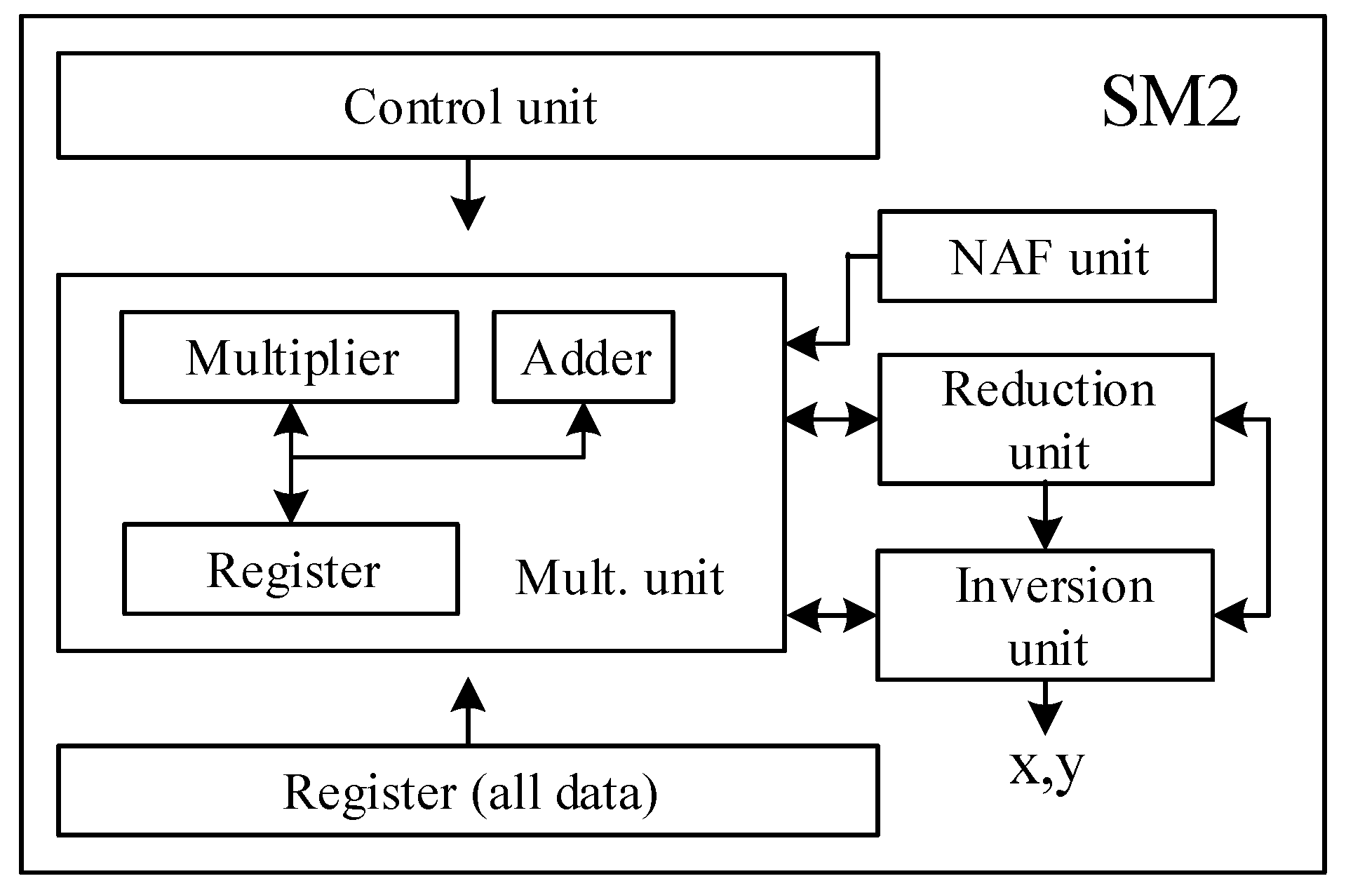
In this section, a SM2 architecture is demonstrated. The block diagram of SM2 is given in Figure 3. The Control unit block is a two-level controller. The top level is responsible for point arithmetic layer including PM, PA and PD operations, and the sublevel is in charge of modular arithmetic layer including MA, MS, MM and MI operations. MM operation is run by the Mult. unit and the NAF unit blocks. The Inversion unit block is applied to coordinate conversion from Jacobian coordinates to affine coordinates at the end of PM operation. For saving hardware footage, the Inversion unit block can also perform the MA/MS operation.
Elliptic curve cryptosystems contain Elliptic Curve Digital Signature Algorithm (ECDSA) signature generation, ECDSA signature verification, and Elliptic Curve Integrated Encryption Scheme (ECIES) encryption and decryption [23]. The PM operation of the architecture here is limited to the SCA-256 prime field. This architecture can also perform PM operation in other specific prime field, if a fast reduction algorithm of other specific prime field is also considered. The architecture we proposed mainly focuses on the acceleration of PM operation, which can be configured to perform the operation at modular arithmetic layer as well. By hardware/software co-design, our hardware module can be used by the software in an embedded system, and the ECC encryption and decryption, signature and verification algorithm can be realized.
4. Hardware Implementation Result
The ECC architecture described above was implemented with Verilog-HDL language. This architecture was synthesized by Synopsys Design Compiler with the SMIC 130-nm CMOS standard cell library. The circuit area was evaluated based on two-way NAND gate. For better comparison, this architecture was also implemented on different Xilinx FPGA boards, including Virtex-6 xc6vlx760, Virtex-5 xc5vfx130t and Virtex-4 xc4vlx200. Xilinx ISE 14.7 was chosen for synthesis, mapping, and routing.
In Algorithm 1, since the results of , , can be pre-calculated, the PM operation took clock cycle as follows:
where m is the length of scalar k, w is the width of NAF, N is the clock cycle for calculating NAF(k), D and A are the clock cycle to perform PD and PA operations, and I stands for the clock cycle of MI operation.
Table 1 shows the clock cycle of each EC operation. The MM operation took five clock cycles. The number of PA operations could be reduced by scalar k being coded by NAF in PM operation. By testing 1000 times, the PM operation required 14,242 clock cycles on average, including the time of coordinate conversion, which took two MI operations.
Table 2 shows the hardware consumption of each block on ASIC platform. The Mult. unit block consists of one 129-bit multiplier, one 512-bit adder and some registers. The Mult. unit block occupies half of the total area, as the table shows, since the multiplier consumes a lot of hardware resources. Table 3 gives the resource utilization on FPGA platform.
Table 4 shows the result of ECC hardware performance comparison among different architecture on ASIC platform. The processor in [3] is designed with a full-word multiplier and took 0.02 ms to perform a PM operation. Although full-word multiplier only needed one clock cycle to perform full multiplication operation, it brought large area consumption and severe latency. This design has a circuit area of 659 k gates, 2.35 times ours, and can run at a frequency of 163.7 MHz, while ours design based on half-word multiplier runs at a frequency of 250 MHz. Our design can run at higher frequency and has better point operational schedules, and the width of NAF w is set to 4 while w is set to 3 in [3]. Therefore, although multiplication operation of our design took five clock cycles, five times that of the method in [3], the PM operation of our design took 2.8 times over the method in [3] but not 5.
In [9,12], the MM and MI operations are based on adder, using interleaved modular multiplication algorithm and binary inversion algorithm. The design in [9] has two multiplier units and two inversion units, whereas the design in [12] combines inversion unit and multiplier unit into one common unit. Therefore, the processor area of the design in [9] is 2.5 times larger than that of the design in [12]. Because their PA and PD operations are implemented in affine coordinates, there are MM and MI operations in PA or PD operations. Since both designs are based on adder, they cost lower areas but more run time of PM operation, reaching 3.01 ms in [9] and 4.07 ms in [12].
The processors proposed in [13,14] employ NAF in PM operation and do not focus on optimizing the operational schedules of PM operation. The processor in [13] employs Montgomery multipliers with sizes ranging from 8-bit × 8-bit to 64-bit × 64-bit. Small size of multiplier results in low hardware consumption but low performance. As a result, this processor costs an area of 120.26k gate, 57.05% less than ours, and requires 2.47 ms, 43 times slower than ours. The processor in [14] is based on a systolic arithmetic unit. It can run at very high frequency of 556 MHz and takes 1.01 ms for one PM operation, 2.65 times faster than the design in [13].
The design we proposed is based on half-word multiplier and the point operational schedules are optimized to increase efficiency. Synthesized with a 130 nm CMOS standard cell library, the area of our design is 280 k gates with PM operation time of 0.057 ms at the frequency of 250 MHz. For parameter , our design is small than [9,12,13,14].
Table 5 shows the performance results on FPGA platform. The designs in [9,10,12,17,18] are all based on adder and have lower performance than our design. The multiplication reported in [9,12] are implemented with interleaved modular multiplication algorithm, that is the simplest multiplication algorithm but costs less adders. Radix-8 booth encoded interleaved modular multiplication algorithm is applied to realize multiplication in [10], while radix-4 booth encoding interleaved modular multiplication algorithm is adopted in [17,18].
Radix-8 booth encoded algorithm is more efficient than radix-8 booth encoded algorithm. Compared with the method in [17,18], the design in [10] achieves a similar PM’s clock cycle (200 k) with less Slices resource (9.37 k). Implemented in Virtex-4 platform, the design in [10] costs 13.158 k Slices and needs 5 ms for PM operation, 7.35 times slower than our design.
NAF point multiplication algorithm is applied in [17] while double-and-always-add point multiplication algorithm is adopted in [18]. Since NAF representation of scalar k has the merits of reducing point multiplication time complexity from to , compared to the design in [17], the design in [18] occupies more LUTs (35.7 k vs. 20.579 k slices on Virtex-4) to attain a similar PM’s clock cycle (207.10 k vs. 191.815 k). On Virtex-5 platform, the design in [17] occupies 31.431 k LUTs and takes 2.62 ms to perform PM operation at a maximum clock frequency of 73 MHz. On Virtex-6 FPGA, the design in [18] occupies 32.4k LUTs and computes PM operation in 1.43 ms operating at a maximum frequency of 144 MHz. Our design was 6.24 times faster than the design in [17] on Virtex-5 platform and 3.86 times faster than the design in [18] on Virtex-6 platform.
The design in [19] is based on the redundant-signed-digit-based parallel programmable unit with four Montgomery multipliers. On Virtex-6 platform, it consumes 44.3 k LUTs and takes 0.65 ms to compute a single PM operation at a maximum frequency of 144.5 MHz. Our design was 1.76 times faster and saved 37.57% LUTs on the same platform. The processor reported in [20] is a LUTs based design for National Institute of Standards and Technology (NIST) recommended prime NIST-256. It takes 0.47 ms to compute a 256-bit PM operation and occupies 65.6 k LUTs on Virtex-6 platform. Our design was 1.27 times faster and saved 57.84% LUTs on the Virtex-6 platform.
Our design took 0.37 ms, 0.77 ms, and 0.64 ms to perform one 256-bit PM operation, and occupied 27.655 LUTs, 26.718 LUTs, and 21.882 k Slices on Virtex-6, Virtex-5, and Virtex-4 platforms, respectively. Compared to the designs shown in Table 5, our architecture achieved higher performance and lower .
5. Conclusions
A high-performance ECC processor over GF(p) is proposed in this paper. Two-stage fast reduction algorithm over SCA-256 is presented to avoid iterative addition/subtraction operations to get the final result, resulting in lower latency and less hardware consumption. Half-word multiplier is chosen to balance area consumption and performance. The PA and PD operational schedules are redesigned to improve the parallelism of MM and MA/MS operations and to maximize hardware reuse. Pipeline design is fully explored to enhance parallel computing of MM operation, and includes both multiplication and fast reduction. The implementation results reveal that the proposed ECC processor offers higher speed over the state-of-the-art ECC processors with just a small area overhead. The processor is better than others since it makes a tradeoff between area and performance.
Author Contributions
Data curation, X.H.; Formal analysis, X.H. and X.Z.; Investigation, X.H. and S.Z.; Methodology, X.H., S.Z., S.C. and X.X.; Software, X.H. and X.Z.; Writing—original draft, X.H.; and Writing—review and editing, W.L., S.C. and X.X.
Funding
This research received no external funding.
Acknowledgments
This work was supported by Science and Technology Planning Project of Guangdong Province of China (2017B010124003 and 2015B010128013).
Conflicts of Interest
The authors declare no conflict of interest.
Abbreviations
The following abbreviations are used in this manuscript:
| ECC | elliptic curve cryptography |
| MM | modular multiplication |
| PM | point multiplication |
| TSFR | two-stage fast reduction |
| NAF | nonadjacent form |
| CMOS | complementary metal oxide semiconductor |
| ECDLP | elliptic curve discrete logarithm problem |
| SCA | State Cryptography Administration |
| FPGA | Field Programmable Gate Array |
| ASIC | Application Specific Integrated Circuit |
| PA | point addition |
| PD | point doubling |
| EC | elliptic curve |
| MI | modular inversion |
| MA | modular addition |
| MS | modular subtraction |
| ECDSA | Elliptic Curve Digital Signature Algorithm |
| ECIES | Elliptic Curve Integrated Encryption Scheme |
| NIST | National Institute of Standards and Technology |
References
- Miller, V.S. Use of elliptic curves in cryptography. In Proceedings of the Annual International Cryptology Conference (CRYPTO), Santa Barbara, CA, USA, 18–22 August 1985; pp. 417–426. [Google Scholar]
- Koblitz, N. Elliptic curve cryptosystems. Math. Comput. 1987, 48, 203–209. [Google Scholar] [CrossRef]
- Zhao, Z.; Bai, G. Ultra High-Speed SM2 ASIC Implementation. In Proceedings of the 2014 IEEE 13th International Conference on Trust, Security and Privacy in Computing and Communications, Beijing, China, 24–26 September 2014; pp. 182–188. [Google Scholar]
- State Cryptography Administration of China. Public Key Cryptographic Algorithm SM2 Based on Elliptic Curves; State Cryptography Administration of China: Beijing, China, 2010. Available online: http://www.oscca.gov.cn/sca/xxgk/2010-12/17/content_1002386.shtml (accessed on 12 April 2019).
- Ghosh, S.; Alam, M.; Gupta, I.S.; Chowdhury, D.R. A Robust GF(p) parallel arithmetic unit for public key cryptography. In Proceedings of the 10th Euromicro Conference on Digital System Design Architectures, Methods and Tools (DSD 2007), Lubeak, Germany, 29–31 August 2007; pp. 109–115. [Google Scholar]
- Guneysu, T.; Paar, C. Ultra High Performance ECC over NIST Primes on Commercial FPGAs. In Proceedings of the International Workshop on Cryptographic Hardware and Embedded Systems, Washington, DC, USA, 10–13 August 2008; Springer: Berlin/Heidelberg, Germany, 2008; pp. 62–78. [Google Scholar]
- McIvor, C.J.; McLoone, M.; McCanny, J.V. Hardware elliptic curve cryptographic processor over GF(p). IEEE Trans. Circuits Syst. I Reg. Pap. 2006, 53, 1946–1957. [Google Scholar] [CrossRef]
- Khan, Z.-U.-A.; Benaissa, M. Throughput/Area-efficient ECC Processor Using Montgomery Point Multiplication on FPGA. IEEE Trans. Circuits Syst. II Express Br. 2015, 62, 1078–1082. [Google Scholar] [CrossRef]
- Ghosh, S.; Alam, M.; Chowdhury, D.R.; Gupta, I.S. Parallel crypto-devices for GF(p) elliptic curve multiplication resistant against side channel attacks. Comput. Electr. Eng. 2009, 35, 329–338. [Google Scholar] [CrossRef]
- Javeed, K.; Wang, X. FPGA Based High Speed SPA Resistant Elliptic Curve Scalar Multiplier Architecture. Int. J. Reconfig. Comput. 2016, 2016, 6371403. [Google Scholar] [CrossRef]
- Sghaier, A.; Zeghid, M.; Massoud, C.; Mahchout, M. Design And Implementation of Low Area/Power Elliptic Curve Digital Signature Hardware Core. Electronics 2017, 6, 46. [Google Scholar] [CrossRef]
- Hu, X.; Zheng, X.; Zhang, S.; Cai, S.; Xiong, X. A Low Hardware Consumption Elliptic Curve Cryptographic Architecture over GF(p) in Embedded Application. Electronics 2018, 7, 104. [Google Scholar] [CrossRef]
- Satoh, A.; Takano, K. A scalable dual-field elliptic curve cryptographic processor. IEEE Trans. Comput. 2003, 52, 449–460. [Google Scholar] [CrossRef]
- Chen, G.; Bai, G.; Chen, H. A High-Performance elliptic curve cryptographic processor for general curves over GF(p) based on a systolic arithmetic unit. IEEE Trans. Circuits Syst. II Express Briefs 2007, 54, 412–416. [Google Scholar] [CrossRef]
- Feng, X.; Li, S. A High Performance FPGA Implementation of 256-bit Elliptic Curve Cryptography Processor Over GF(p). Ieice Trans. Fundame. 2015, E98.A, 863–869. [Google Scholar] [CrossRef]
- Marzouqi, H.; Al-Qutayri, M.; Salah, K. Review of Elliptic Curve Cryptography processor designs. Microprocess. Microsyst. 2015, 39, 97–112. [Google Scholar] [CrossRef]
- Javeed, K.; Wang, X.; Scott, M. High performance hardware support for elliptic curve cryptography over general prime field. Microprocess. Microsyst. 2016, 51, 331–342. [Google Scholar] [CrossRef]
- Javeed, K.; Wang, X. Low latency flexible FPGA implementation of point multiplication on elliptic curves over GF(p). Int. J. Circuit Theory Appl. 2017, 45, 214–228. [Google Scholar] [CrossRef]
- Ali, S.Y.; Khalid, J.; Shoaib, A.; Wang, X. A high-speed RSD-based flexible ECC processor for arbitrary curves over general prime field. Int. J. Circuit Theory Appl. 2018, 46, 1858–1878. [Google Scholar]
- Shah, Y.A.; Javeed, K.; Azmat, S.; Wang, X. Redundant Signed Digit based High Speed Elliptic Curve Cryptographic Processor. J. Circuits Syst. Comput. 2018. [Google Scholar] [CrossRef]
- Montgomery, P.L. Modular multiplication without trial division. Math. Comput. 1985, 44, 519–521. [Google Scholar] [CrossRef]
- Amanor, D.N.; Paar, C.; Pelzl, J.; Bunimov, V. Efficient Hardware Architectures for Modular Multiplication on fpgas. In Proceedings of the International Conference on Field Programmable Logic and Applications, Tampere, Finland, 24–26 August 2005. [Google Scholar]
- Hankerson, D.; Vanstone, S.; Menezes, A. Guide to Elliptic Curve Cryptography; Springer: New York, NY, USA, 2004. [Google Scholar]
- Solinas, J.A. Efficient Arithmetic on Koblitz Curves. Des. Codes Cryptogr. 2000, 19, 195–249. [Google Scholar] [CrossRef]
- Karatsuba, A. Multiplication of multidight numbers on automata. Doklady Akad Nauk SSSR 1963, 7, 145. [Google Scholar]
Figure 1.
Multiplication operational schedule between existing structure and our structure.

Figure 2.
Operational schedule without idle clock cycle: (a) point addition; (b) point doubling; (c) between point addition and point doubling; and (d) between point doubling and point doubling.
Figure 2.
Operational schedule without idle clock cycle: (a) point addition; (b) point doubling; (c) between point addition and point doubling; and (d) between point doubling and point doubling.

Figure 3.
SM2 Architecture diagram.


Table 1.
The clock cycle of EC operations.
| Operation | Clock Cycle | Operation | Clock Cycle | Operation | Clock Cycle |
|---|---|---|---|---|---|
| MA | 1 | NAF(k) | 120 | MI | 540 |
| MS | 1 | PA | 56 | PM | 14242 |
| MM | 5 | PD | 40 |
Table 2.
Hardware consumption of each block on ASIC platform.
| Block | Mult. Unit | Reduction Unit | NAF Unit | Inversion Unit | SM2 (Total) |
|---|---|---|---|---|---|
| area (gate) | 141,661 | 22,417 | 14,913 | 29,226 | 280,137 |
| Percent (%) | 50.57 | 8.00 | 5.32 | 10.43 | - |
Table 3.
Resource utilization on FPGA platform.
| Resource | Slice LUTs | Flip Flops | DSP | Slice |
|---|---|---|---|---|
| Virtex-6 | 27,662 | 11,911 | 80 | 10,089 |
| Virtex-5 | 26,717 | 11,596 | 80 | 7943 |
| Virtex-4 | 40,817 | 14,173 | 78 | 22,242 |
Table 4.
ECC hardware performance comparison on ASIC platform.
| Design | Platform | Prime Field | Frequency (MHz) | Clock Cycle (k) | Area (k Gate) | PM * (ms) | |
|---|---|---|---|---|---|---|---|
| This work | 0.13-m | SCA-256 | 250 | 14.24 | 280 | 0.057 | 15.96 |
| 3 | 0.13-m | SCA-256 | 163.7 | 3.3 | 659 | 0.02 | 13.28 |
| 9 | 0.13-m | 256 | 110 | - | 167.5 | 3.01 | 504 |
| 12 | 0.13-m | 256 | 150 | 610 | 57.05 | 4.07 | 232 |
| 13 | 0.13-m | 256 | 137.7 | 340 | 120.26 | 2.47 | 297 |
| 14 | 0.13-m | 256 | 556 | 562 | 122 | 1.01 | 123 |
AT: Area * PM, area-time product.
Table 5.
ECC hardware performance comparison on FPGA platform.
| Design | Platform | Prime Field | Frequency (MHz) | Clock Cycle (k) | Area | PM (ms) | TP (ops) | |
|---|---|---|---|---|---|---|---|---|
| This work | Virtex-6 | SCA-256 | 38.045 | 14.24 | 27.655k LUTs | 0.37 | 10.35 | 2672 |
| Virtex-5 | 34.15 | 26.717 LUTs | 0.42 | 11.14 | 2398 | |||
| Virtex-4 | 20.87 | 22.242 Slice | 0.68 | 15.18 | 1466 | |||
| 9 | Virtex-4 | 256 | 43 | 331 | 20.123k Slices | 7.7 | 154.95 | 130 |
| 10 | Virtex-4 | 256 | 40 | 200 | 13.158k Slices | 5 | 65.79 | 200 |
| 12 | Virtex-4 | 256 | 20.44 | 610 | 9.37k Slices | 29.84 | 279.61 | 34 |
| 17 | Virtex-5 | 256 | 73 | 191.815 | 31.431k LUTs | 2.62 | 82.35 | 382 |
| Virtex-4 | 49 | 20.579k Slices | 3.91 | 80.46 | 256 | |||
| 18 | Virtex-6 | 256 | 144 | 207.10 | 32.4k LUTs | 1.43 | 46.33 | 699 |
| Virtex-4 | 70 | 35.7k Slices | 2.96 | 105.67 | 337 | |||
| 19 | Virtex-6 | 256 | 221 | 144.5 | 44.3k LUTs | 0.65 | 28.80 | 1538 |
| Virtex-5 | 172 | 44.6k LUTs | 0.84 | 37.46 | 1190 | |||
| Virtex-4 | 141 | 78.5k LUTs | 1.02 | 80.07 | 980 | |||
| 20 | Virtex-6 | NIST-256 | 327 | 153.16 | 65.6k LUTs | 0.47 | 30.83 | 2128 |
| Virtex-5 | 255 | 65k LUTs | 0.6 | 39.00 | 1666 | |||
| Virtex-4 | 191 | 96.6k LUTs | 0.8 | 77.28 | 1250 |
© 2019 by the authors. Licensee MDPI, Basel, Switzerland. This article is an open access article distributed under the terms and conditions of the Creative Commons Attribution (CC BY) license (http://creativecommons.org/licenses/by/4.0/).
Share and Cite
MDPI and ACS Style
Hu, X.; Zheng, X.; Zhang, S.; Li, W.; Cai, S.; Xiong, X. A High-Performance Elliptic Curve Cryptographic Processor of SM2 over GF(p). Electronics 2019, 8, 431. https://doi.org/10.3390/electronics8040431
AMA Style
Hu X, Zheng X, Zhang S, Li W, Cai S, Xiong X. A High-Performance Elliptic Curve Cryptographic Processor of SM2 over GF(p). Electronics. 2019; 8(4):431. https://doi.org/10.3390/electronics8040431
Chicago/Turabian StyleHu, Xianghong, Xin Zheng, Shengshi Zhang, Weijun Li, Shuting Cai, and Xiaoming Xiong. 2019. "A High-Performance Elliptic Curve Cryptographic Processor of SM2 over GF(p)" Electronics 8, no. 4: 431. https://doi.org/10.3390/electronics8040431
Note that from the first issue of 2016, this journal uses article numbers instead of page numbers. See further details here.