Article

Analysis and Experimental Test of Electrical Characteristics on Bonding Wire

School of Electro-Mechanical Engineering, Xidian University, Number 2 Taibai South Road, Xi’an 710071, China
*
Author to whom correspondence should be addressed.
Electronics 2019, 8(3), 365; https://doi.org/10.3390/electronics8030365
Submission received: 20 February 2019 / Revised: 22 March 2019 / Accepted: 23 March 2019 / Published: 26 March 2019
(This article belongs to the Special Issue Applications of Electromagnetic Waves)

Abstract

:
In this paper, electrical characteristic analysis and corresponding experimental tests on gold bonding wire are presented. Firstly, according to EIA (Electronic Industries Association)/JEDEC97 standards, this paper establishes the electromagnetic structure model of gold bonding wire. The parameters, including flat length ratio, diameter, span and bonding height, were analyzed. In addition, the influence of three kinds of loops of bonding wire is discussed in relation to the S parameters. An equivalent circuit model of bonding wire is proposed. The effect of bonding wire on signal transmission was analyzed by eye diagram as well. Secondly, gold bonding wire design and measurement experiments were implemented based on radio frequency (RF) circuit theory analysis and test methods. Meanwhile, the original measurement data was compared with the simulation model data and the error was analyzed. At last, the data of five frequency points were processed to eliminate the fixture error as much as possible based on port embedding theory. The measurement results using port extension method were compared with the original measurement data and electromagnetic field simulation data, which proved the correctness of the simulation results and design rules.

1. Introduction

Electronic packaging is the connection between the chip and the external pin. It is an important part for maintaining the electrical, thermal and mechanical properties of the device. Electronic components are developing towards being small volume, high power, high frequency and highly reliable, which requires higher packaging techniques. However, packaging technology has gradually become a bottleneck in the development of semiconductor industry. Although there are advanced package forms such as flip-chip, tape automated bonding, and wafer level package, more than 90% of the device packages are still using wire bonding (WB). Therefore, WB is the dominant form of electronic packaging for its mature technology, low cost and high reliability [1]. Precious metal bonding wires are key materials in electronic packaging including gold bonding wire, copper bonding wire, sliver bonding wire and composite metal bonding wire. Currently, semiconductor packaging is using gold wire bonding as the main connection from the chip to the lead frame or substrate. The high price of gold wire has led to the development of bonding wire made from copper silver and palladium-coated-copper as lower cost alternatives. So far, gold wire accounts for the highest proportion of bonding wire in high-end electronic products because of its stable chemical properties, good ductility and excellent weldability. According to authoritative prediction and a realistic encapsulation of the industry situation, WB will still be the main interconnection method of electronic products until 2020 and will continue developing [2].
In the package structures, bonding wire can be used as signal transmission line, power, grounding and so on. With the improvement of the transmission signal frequency (currently the system operating frequency up to GHz), bonding wire is no longer a simple transmission line. Moreover, it performs like radio frequency (RF) in a variety of ways, such as crosstalk, coupling, distortion, parasitism, ground bounce, interference and other electromagnetic phenomena [3]. Therefore, how to solve the electrical problems and improve the signal transmission quality of the gold bonding wire in circuit design, analysis and testing have become research hotspots. At present, research on the electrical properties in WB packaging is mainly focused on the following aspects: (1) the process and geometric parameters of bonding wire such as bonding process, bonding wire loop parameters, materials and so forth [4,5,6,7]; (2) the wiring form of bonding wire including wire spacing, signal pin distribution, interconnection etc., [8,9,10,11]; (3) the overall package design such as grounding copper cover, through silicon vias (TSV) technology, and the redistribution layer (RDL) of flip chip or the like [12,13,14,15]. Zhang analyzed the influence of bonding wire on parasitic parameters under different span and arch height. The larger the span and arch height, the greater the influence on the circuit characteristics by simulation [16]. Lu investigated the relationship between materials with different dielectric constants and return losses, but the geometric parameters of bonding wire were not taken into consideration, unfortunately [17]. Liang studied the height arch of single gold bonding wire and the results showed that the lower the arch height of bonding gold wire the better in the case of single gold and the same span. But the value of high arches in the simulation cannot guarantee the welding stability of flat bonding gold because of the characteristics of bonding process [18]. Owing to the diversity of the IC products and package types, there are still no satisfactory results on effects such as wire loops, geometric parameters, electromagnetic models, overall package design and other factors on comprehensive IC electromagnetic properties.
In this paper, the electromagnetic properties of bonding wire are studied. The transmission performance of bonding wire is analyzed based on the electromagnetic field model. The design rule is derived from the simulation result. Furthermore, the WB and measurement experiments are designed. The experimental data and simulation data are compared. The error is also analyzed. Finally, the correctness of the simulation is proved by comparison with other experiments, which provides the theoretical basis for the bonding wire selection and design in high frequency.

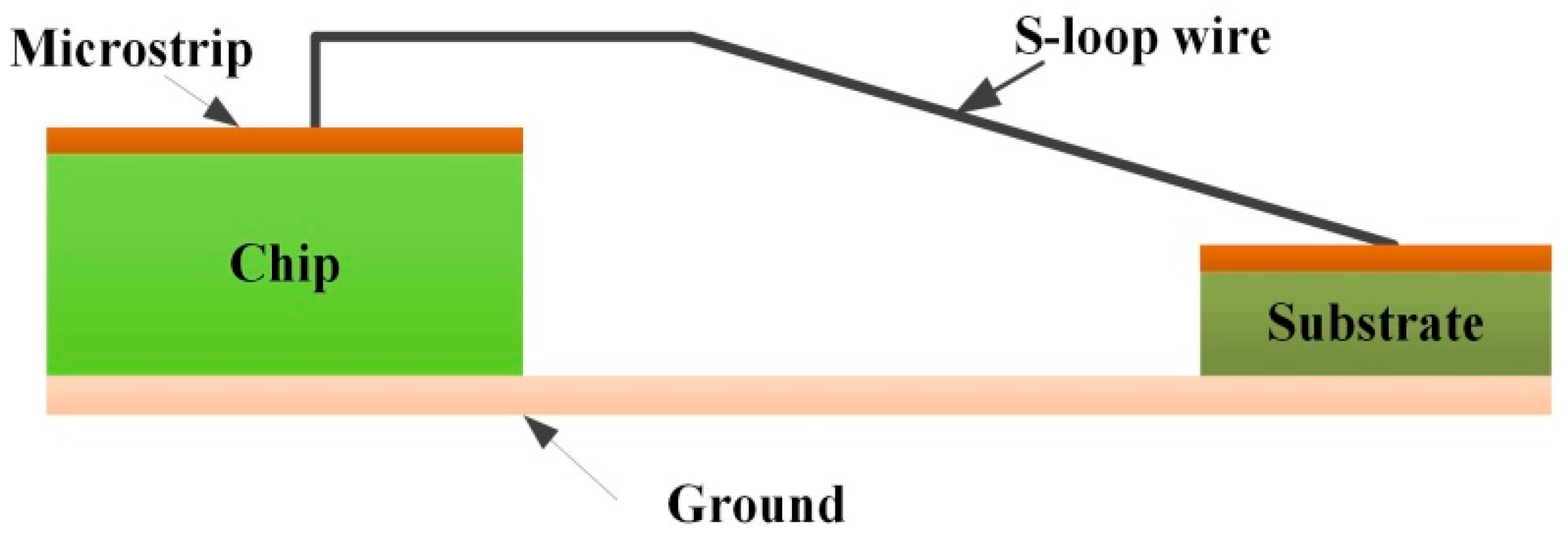
2. Bonding Wire Model

Figure 1 shows the package structure of a ball grid array (BGA) composed of a BGA solder ball, PCB board, lead frame, chip, gold bonding wires, epoxy resin encapsulation and so on. In addition, bonding wire can be used as signal transmission line, power, and grounding. In low frequency signal, the bonding wire is equivalent to a line without resistance, capacitor, or inductive transmission. However, in high frequency, the electrical properties of bonding wire have an important influence on the performance of the whole structure and even the circuit. On the one hand, the influence of the parasitic parameters of the bonding wire on the circuit cannot be ignored. At the same time, the inductance, resistance and capacitance (RLC) parameters of bonding wire are constantly changing because of the skin effect with frequency. On the other hand, the cumulative effect of many bonding wires greatly influences the signal transmission capacity, especially in high frequency system. Once the poor WB transmission performance affects the signal transmission and cause large signal loss, it may easily lead to signal crosstalk and other serious signal integrity problems.

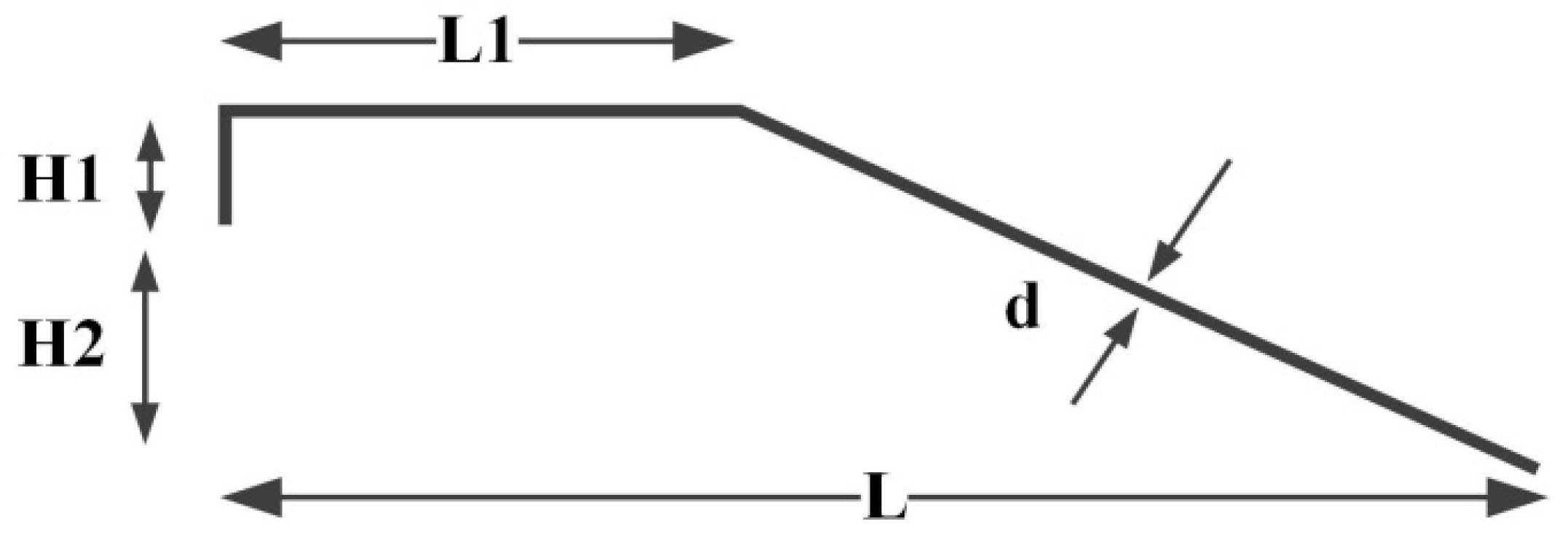
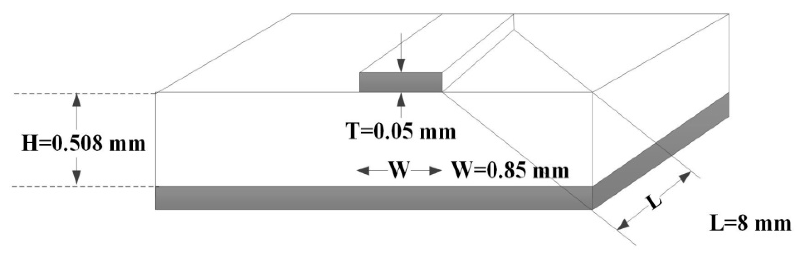
2.1. Geometric Parameters

S-loop wire is the most common bonding wire. S-loop wire that has a longer flat distance then breaks is mainly used in two conditions: when the actual loop length of wire is too long, or the welding wire arc height should be under control in some devices. S-loop can prevent the sweep and sag problem when epoxy compound flows during the transfer injection molding process because of its strong stability and stiffness. The geometric parameters of the S-loop wire are shown in Figure 2 (d is the diameter, L is the span, L1 is the flat distance of S-loop wire, H1 is the bonding height of the arch and H2 is the connection height).
In this section, the influence of the geometrical parameters on the scattering parameters is discussed. The four geometric parameters factors are the ratio of the L1/L, the diameter d, the span L and the bonding height H1. Finally, by comparing the scattering parameters, the transmission characteristics of Q-loop, S-loop and M-loop are analyzed and derived.

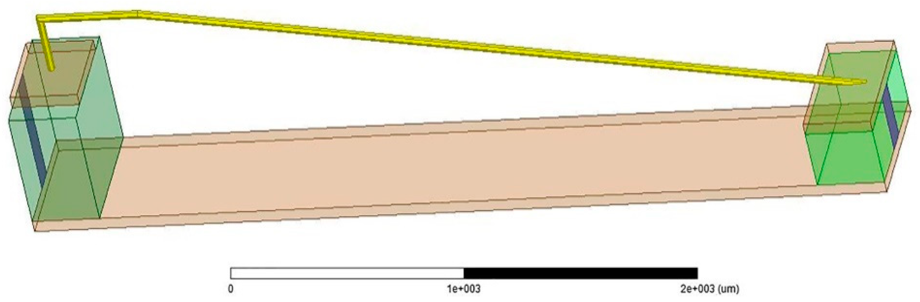
2.2. Simulation Model of Single Gold Bonding Wire

The simulation model of single bonding wire (as shown in Figure 3 was composed using S-loop wire, microstrip lines, chips, substrate and ground. In practice, the bonding wire was embedded in a plastic body. The plastic material was not taken into consideration in order to simplify this model. In actual work conditions, bonding wire usually connects the chip I/O pin to the other chip pins or the external PCB board. Therefore, the two ends of the bonding wires were connected to different materials. This meant that the dielectric constant and the dielectric thickness were different. As the simulation frequency is up to GHz level, Rogers RO4350B was chosen as the substrate in order to reduce substrate dielectric loss. The materials of each part in the simulation model are shown in Table 1. The ambient temperature can be maintained at a constant and the loss factor of materials ignored as well.

2.3. Solve Setting

The bonding wire models with different geometric parameters were established by using HFSS (High Frequency Structure Simulator) electromagnetic field simulation software. After adding the radiation boundary condition and the port excitation, the corresponding analysis was set to solve the frequency of the simulation. The return loss (S11) and insertion loss (S21) of different geometric parameters models were obtained after simulation. The HFSS simulation model is shown in Figure 4. The total port excitations were set respectively on the two sides of the bonding wire. The simulation frequency was from 1MHz to 20 GHz and the logarithmic scale was used to solve the step. In this paper, skin effect can be ignored as a secondary factor. The electrical performance of the bonding wire was obtained and analyzed by using the terminal-driven solution.

3. Frequency Domain Simulation

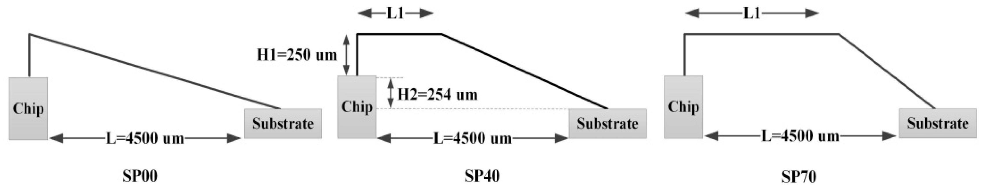
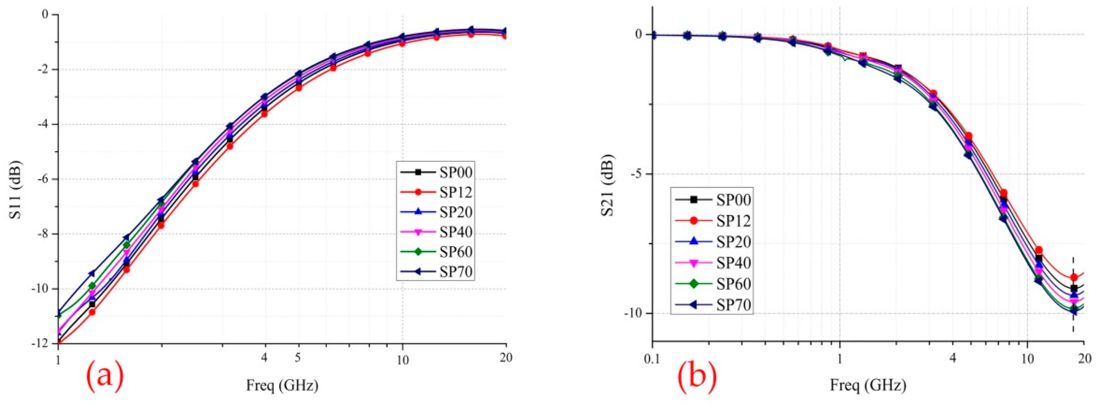
3.1. Influence of Flat Length Ratio on S Parameter of Bonding Wire

S-loop wire is the most common bonding wire. Due to its flat length, S-loop wire can withstand the impact from the epoxy compound in plastic molding process and prevent the gold bonding wire from having a horizontal sweep and vertical sag problem. However, too long a length of flat length wire will bring serious signal crosstalk and coupling problems. According to the Kulicke and Soffa package model library in Cadence APD, WL_LH3_SPXX series of models were selected for modeling and simulation. The value after SP is the ratio of the flat length with span, that is, the value of L1/L (as shown in Figure 5). According to the standard, there are six sizes in total: 00, 12, 20, 40, 60 and 70.
According to the geometric relationship shown in Figure 5, the parameters of the model were selected (L = 4500 μm, H1 = 250 μm, H2 = 254 μm, d = 25 μm). The ratios of the flat length to the span L are 0, 12%, 20%, 40%, 60% and 70%, respectively through changing the length of L1, while sweep frequency ranges from 1 MHz to 20 GHz. The results of S11 and S21 with the ratio and frequency of the bonding wire are shown in Figure 6a,b respectively.
In order to get a clear graph and accurate data, the S11 log coordinate was set from 1 to 20 GHz. The return loss describes the signal reflection performance of the transmission line. The smaller return loss means less signal loss and better signal integrity performance. From Figure 6, it can be seen that the loss increases with the frequency. In addition, the SP12 bonding wire has a higher cutoff frequency, which demonstrates that it can work in a higher frequency band. Compared with SP70 bonding wire, the working frequency increases by 16% (0.64 GHz). Figure 7 shows S21 (insertion loss) parameters. The abscissa is set from 0.1 to 20 GHz. It can be found that the insertion loss also increases with frequency, which suggests the ratio of the signal power delivered to the terminal prior to insertion versus the signal power delivered to the terminal after insertion is constantly decreasing. The value of the minimum point of S21 and its corresponding frequency under the condition of different flat length are selected in Table 2. The minimum point indicates the signal transmission is the worst when the ratio of the passing and input signal reaches the minimum. It is easy to get from Table 2 that the minimum values of S21 in SP12 are larger than that in other cases. At 17.38 GHz, the modulus of S21 reaches 8.71, which increases by 13.9% compared with SP70. According to the definition of S21, the ratio of passing signal with incoming signal is 36.69% after calculation.

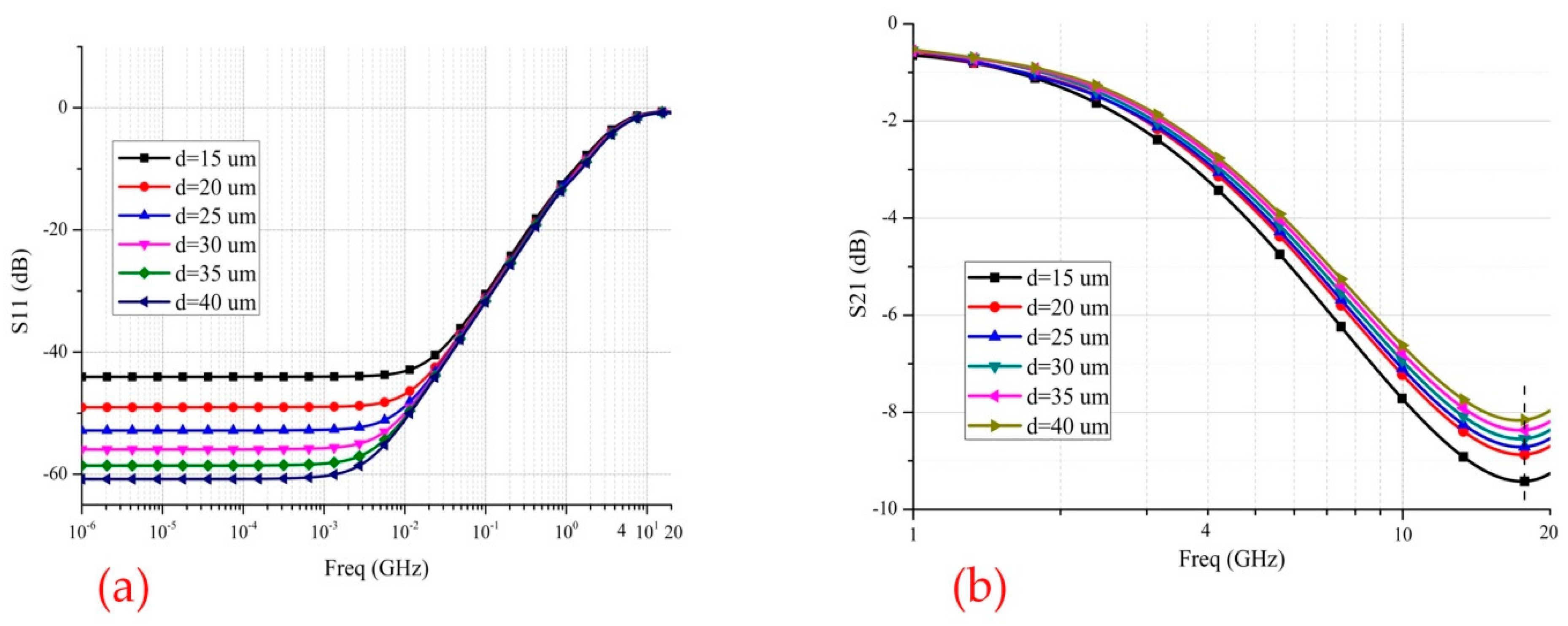
3.2. Influence of Diameter on S Parameter of Bonding Wire

Considering the density of the pins connection, the diameter of the bonding wire is an important design parameter. Six kinds of nominal diameters of bonding wire were selected for simulation: 15 μm, 20 μm, 25 μm, 30 m, 35 μm and 40 μm. Taking the SP12 bonding wire as a model, the span of L was 4500 μm and the connection height of H1 was 250 μm. The other simulation parameters were kept constant, while the diameter of d was chosen as the variable. The sweep frequency ranges from 1MHz to 20 GHz. The results of the S11 and S21 with the diameter and frequency of the bonding wire are shown in Figure 7a,b.
Figure 7a is the logarithmic coordinate graph of S11. It can be easily seen that the return loss grows with increase of frequency. For example, the bonding wire with a diameter of 40 μm can operate at the near 5 GHz frequency. Compared with the diameter of 15 μm, the working frequency band increased by 17.5% (0.73 GHz,). Figure 7b is the logarithmic coordinate graph of S21. With the increase of frequency, the insertion loss rises, while the signal transmission performance decreases. The S21 extreme points of different diameters were extracted as shown in Table 3. When the diameter was 40 μm (17.18 GHz), S21 had the minimum value of −8.16 dB, and the ratio of passing with incoming signal was 39.06%. Compared with the diameter of 15 μm, the modulus of S21 went up by 1.26 dB (about 15.4%). Also, the signal transmission quality increased by 5.26%.

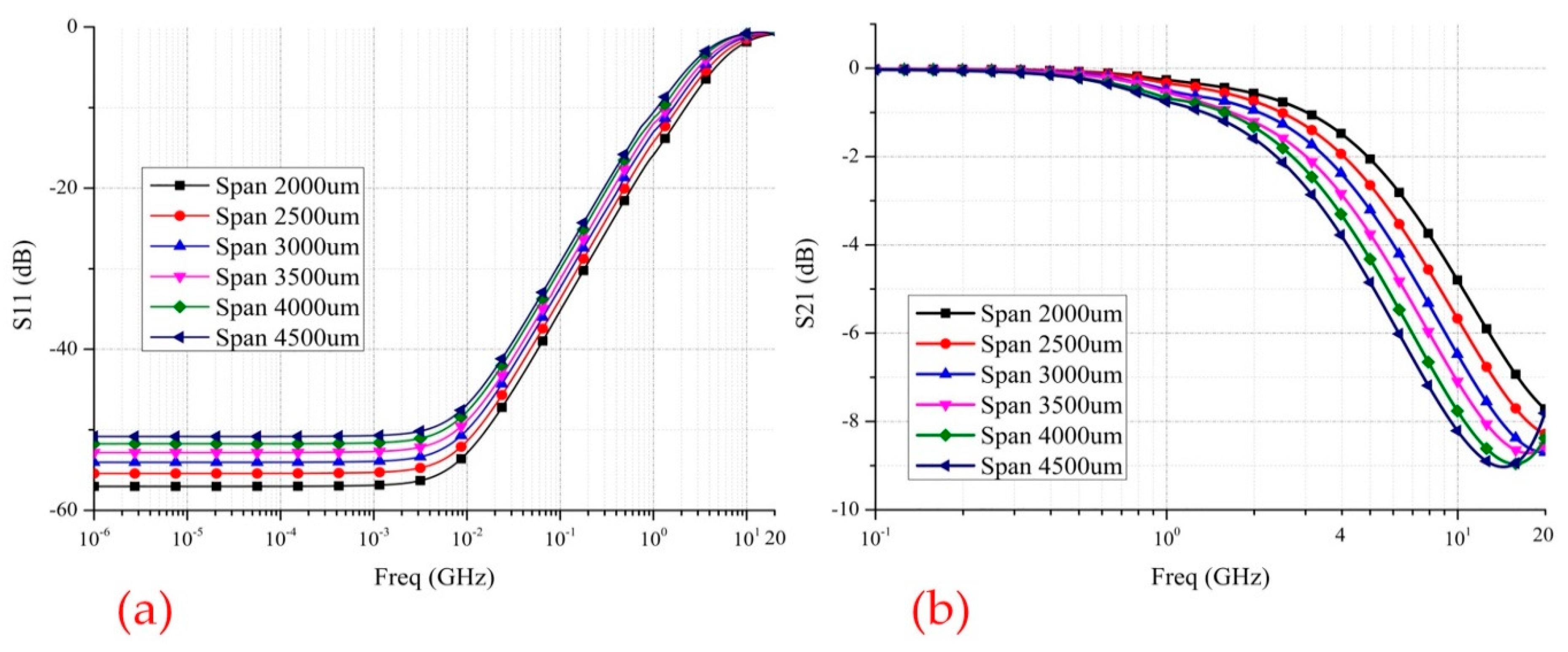
3.3. Influence of Span on S Parameter of Bonding Wire

With the development of the narrow spacing (fine-pinch) and the stacked package, the ratio of low radian and long span bonding wire are also rising. The span L is the horizontal distance of interconnection, which is the most important geometric parameter in the bonding wire. While keeping the other parameters unchanged, the bonding wire span L was selected as a variable. The span scanning ranged from 2000 μm to 4500 μm. In addition, the interval was 500 μm: 2000 μm, 2500 μm, 3000 μm, 3500 μm, 4000 μm and 4500 μm. The sweep frequency ranged from 1 MHz to 20 GHz. The results of S11 and S21 with the span and frequency of the bonding wire are shown in Figure 8a,b ranging from 1MHz to 20 GHz.
According to the trends of return loss and graph of insertion loss, the transmission quality of the signal decreases with the rise of the span because of the increase of the span and the length of the bonding wire. Figure 8a is the logarithmic graph of return loss S11. Taking half the power point as an example, when the longitudinal coordinate was −3 dB, the horizontal coordinate of span 2500 μm bonding wire stood at 7 GHz, while the coordinate of span 5000 μm was 3.65 GHz. The working frequency also increased by 91%. In the insertion loss graph, the working band of the bonding wire with a span of 2500 μm was higher than 3.36GHz in the −3 dB (101%). Figure 8b is the insertion loss S21 logarithmic coordinate graph. With the increase of frequency, the insertion loss grows and the signal transmission performance drops. The S21 extreme points of different spans were extracted (as shown in Table 4). When the span was 2500 μm at 25.12 GHz, the S21 had the minimum value of −8.01 dB, and the ratio of passing with incoming signal was 39.76%. Compared with the case of the 5000 μm, the modulus of S21 increased by 0.98 dB (about 12.2%). The signal transmission quality grew by 4.4%, and the corresponding frequency of the extreme point increased by 10.79 GHz.

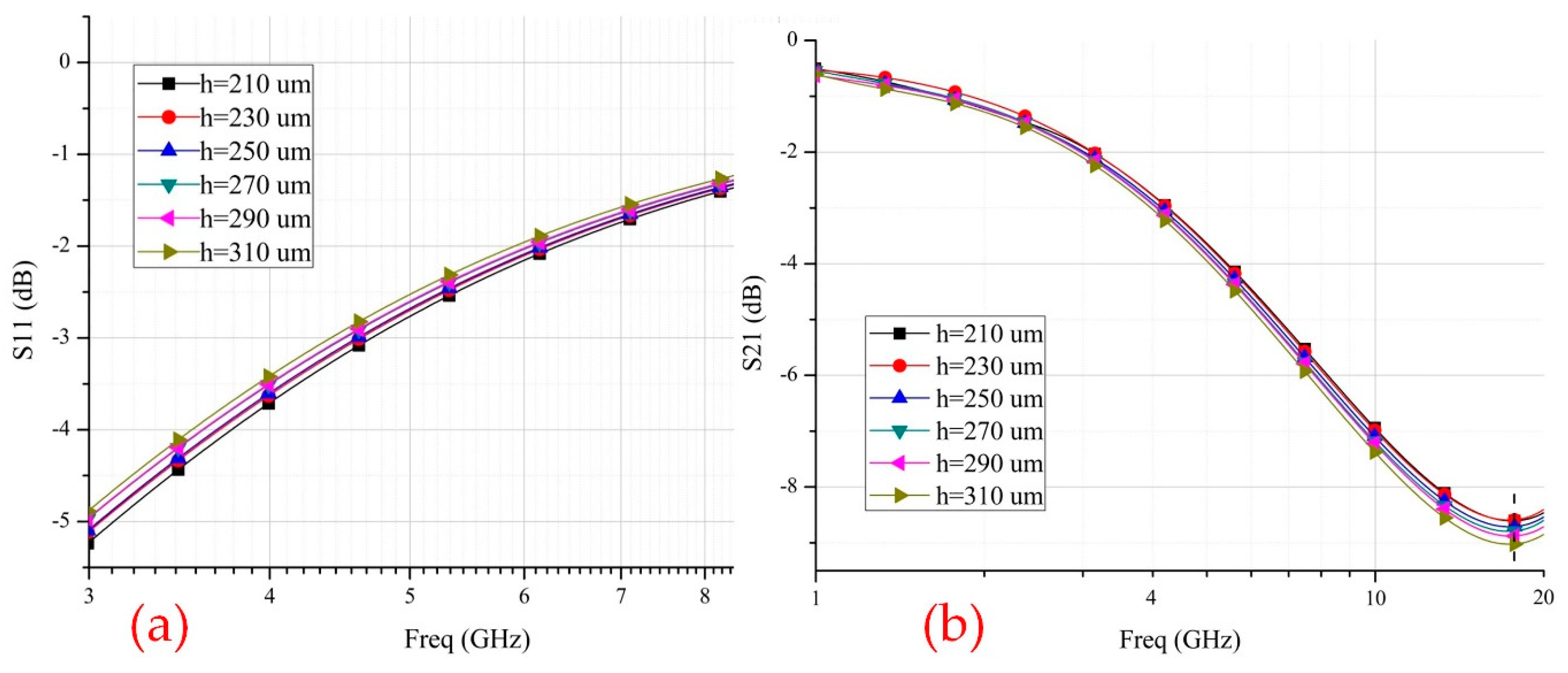
3.4. Influence of Bonding Height on S Parameter of Bonding Wire

The height of the bonding wire and the arch has a great influence on the electrical properties of the bonding wire. The signal transmission path also increases because of the rise of the height, which exacerbates the signal transmission loss. Keeping the other parameters unchanged, the bonding height of H1 was chosen as the variable. The bonding height scanning ranged from 210 μm to 310 μm, and the interval was 20 μm: 210 μm, 230 μm, 250 μm, 270 μm, 290 μm and 310 μm. The sweep frequency ranged from 1 MHz to 20 GHz. The results of S11 and S21 with the bonding height and frequency of the bonding wire are shown in Figure 9a,b ranging from 1 MHz to 20 GHz.
In order to get clear graph and accurate data, the S11 log coordinate was intercepted from three to 10 GHz in Figure 9a. With the increase of frequency, the return loss also increased. Furthermore, the wire with a smaller bonding height had better electrical performance. For example, when the longitudinal coordinate was −3 dB, the corresponding abscissa of bonding wire with height 210 μm was 4.69 GHz, and the abscissa of bonding wire with 310 μm is 4.40 GHz. Figure 9b is the logarithmic coordinate graph of insertion loss S21. The S21 extreme points of different bonding height are extracted in Table 5. When the bonding height was 210 μm, the S21 had the minimum value of −8.61 dB at 17.58 GHz, and the ratio of passing with incoming signal was 37.11%. Compared with the case of 310 μm, the modulus of S21 increased by 0.41 dB (about 4.8%). The signal transmission quality also rises by 1.71%. Although the increase of bonding height will cause the rise of the whole wire length and a decrease in signal quality, the connection height cannot be over reduced. A low height connection will increase stress of bonding wire, making the solder joint unstable and causing other mechanical problems.

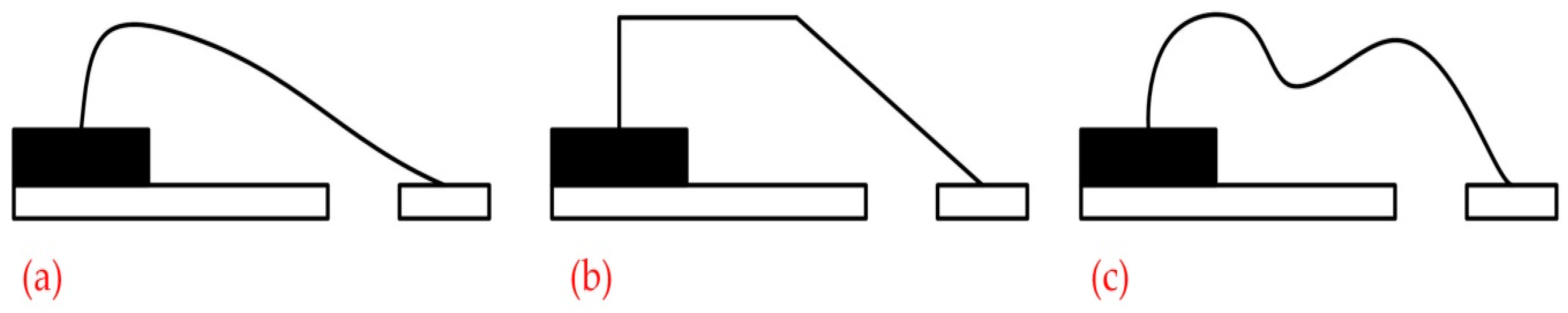
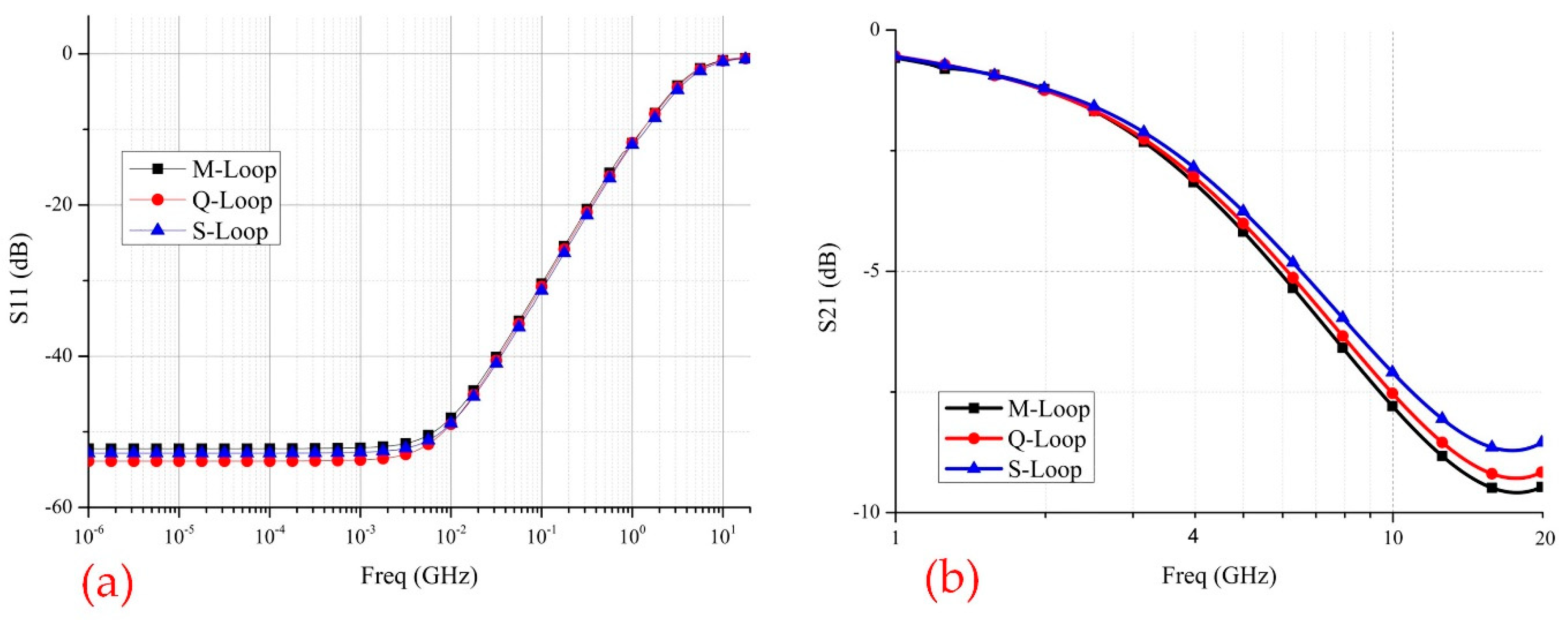
3.5. Influence Of Three Loops On S Parameter Of Bonding Wire

Q-loop, S-loop and M-loop bond modes are shown in Figure 10. The Q-loop is the most universal bonding wire form. Compared with the Q-loop, the S-loop has a longer flat distance. The M-loop bond has the most kinking points. Through the finite element analysis and experimental verification, the result shows that the M-loop is 13–75% as good as the S-loop [19], which suggests that the sweep resistance is better than the S-loop relying on bond span and height. This is because the M-loop bond has five kinking nodes. During the transfer molding process, the M-loop bond has higher stiffness to resist the deformation when epoxy compound flows. Keeping the diameter, span and bonding height unchanged, the S parameters of three kinds of loop wires in 1 MHz–30 GHz are simulated and compared. The results of the 1 MHz–20 GHz scan are shown in Figure 11a,b.
The results of the return loss S11 from 1MHz to 1GHz are shown in Figure 11a. As shown in Figure 11a, the return loss S11 of three different loop modes has little difference. Figure 11b is the logarithmic coordinate graph of the insertion loss S21. It can be seen that the electrical performance of the S-loop wire is the best, while the Q type is slightly worse than that and the M type is the worst in Figure 11b. For example, the working frequency of S type wire increases by 0.32 GHz (about 8%) compared with M-loop wire at −3 dB. The S21 extreme points of different bonding height were extracted in Table 6. For the S type bonding wire, S21 has the minimum value of −8.71 dB at 17.38 GHz, and the ratio of passing and incoming signal is 36.69%. Compared with the case of the M type wire, the modulus of S21 rises by 0.88 dB (about 10.1%), and the signal transmission quality increases by 3.54%. Therefore, reasonable bonding wire modes should be made according to the process and mechanical reliability requirements comprehensively.

3.6. Design Rules

With the increase of the frequency, the bonding parameters have a great influence on the characteristics of microwave transmission. Therefore, it is important to analyze, optimize and design the parasitic characteristics of high-power bonding wires under high frequency. The appropriate design parameters should be selected according to different working frequency bands. When the working frequency is too high, the transmission quality of the signal may be very poor. Combined with the practical project application, in order to reduce the parasitic characteristics while improving the frequency characteristics and electromagnetic properties of bonding wires, the optimization measures are obtained from the following five aspects (as shown in Table 7).

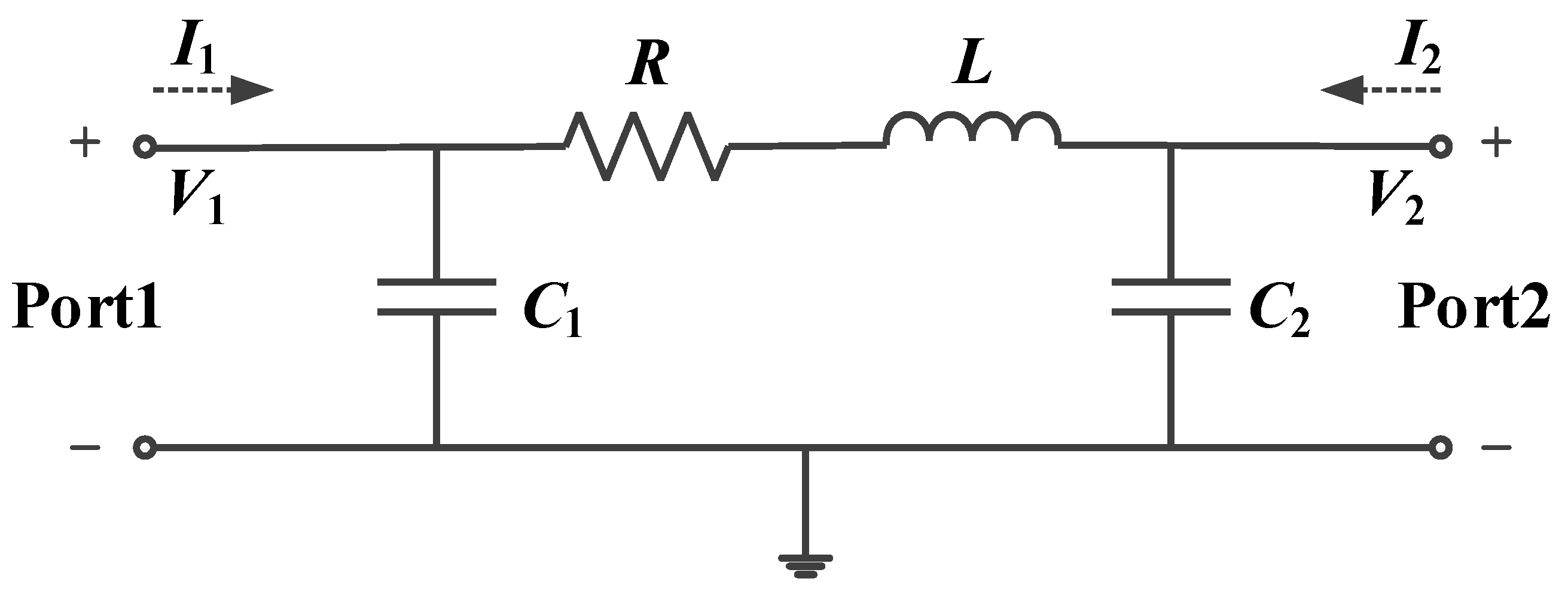
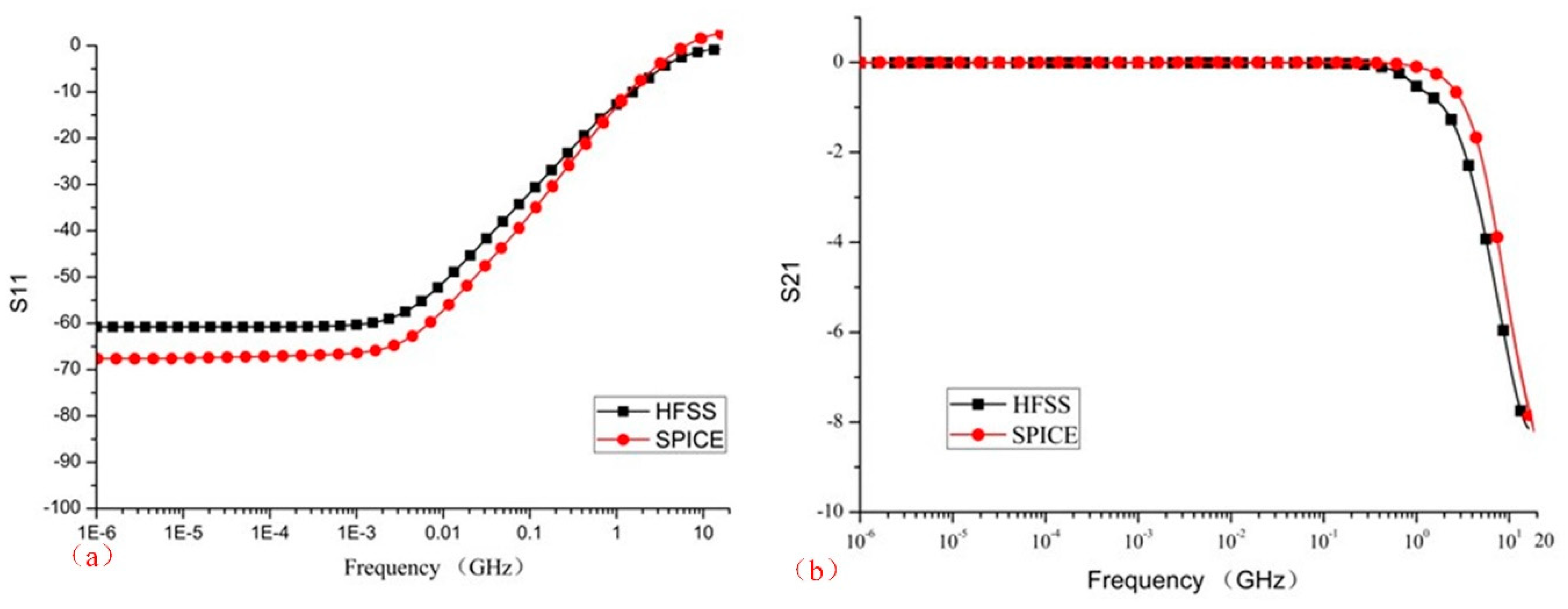
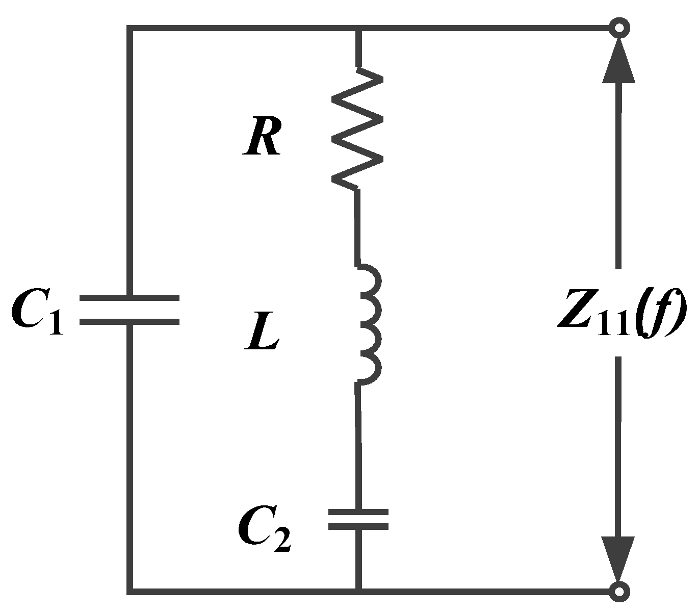
3.7. SPICE Equivalent Circuit Model Of Bonding Wire

As is shown in Figure 12, the SPICE (simulation program with integrated circuit emphasis) equivalent circuit model of bonding wire consists of resistance R, inductance L and two different capacitors C1 and C2. The resistance R and the inductance L are related to the parameters of the bonding wire itself. The two ends of bonding wires are connected to different materials. Therefore, the equivalent capacitance C at the ends of the bonding wire is not the same.
In Figure 12, There are four variables; V1, V2, I1 and I2. Based on Two Port Network Theory, the following equations can be obtained:
{ V 1 = I 1 Z 11 + I 2 Z 12 V 2 = I 1 Z 21 + I 2 Z 22
In this case the relationship between the port currents, port voltages and the Z-parameter is given by:
Z 11 = V 1 I 1 | I 2 = 0 , Z 12 = V 1 I 2 | I 1 = 0 Z 21 = V 2 I 1 | I 2 = 0 , Z 22 = V 2 I 2 | I 1 = 0
Figure 13 shows the equivalent impedance model of Z11. Taking Z11 as an example, the following equations can be obtained through math deduction.
Z 11 ( ω ) = Z 11 ( s ) | s = j ω = R C 2 ω + j ( L C 2 ω 2 1 ) ω ( L C 1 C 2 ω 2 + C 1 + C 2 + j R C 1 C 2 ω )
Similarly, other parameters can be derived as follows:
Z 22 ( ω ) = Z 22 ( s ) | s = j ω = R C 1 ω + j ( L C 1 ω 2 1 ) ω ( L C 1 C 2 ω 2 + C 1 + C 2 + j R C 1 C 2 ω )
Z 12 ( ω ) = Z 21 ( ω ) = Z 12 ( s ) | s = j ω = 1 ω [ j L C 1 C 2 ω 2 R C 1 C 2 ω + j ( C 1 + C 2 ) ]
Based on the principle of RF circuit, the two-port S parameters can be obtained from the equivalent two-port Z parameters by means of the following expressions:
S 11 ( ω ) = [ Z 11 ( ω ) Z 0 ] [ Z 22 ( ω ) + Z 0 ] Z 12 ( ω ) Z 21 ( ω ) [ Z 11 ( ω ) + Z 0 ] [ Z 22 ( ω ) + Z 0 ] Z 12 ( ω ) Z 21 ( ω ) = 2 [ R + Z 0 ( 1 L C 2 ω 2 ) + j ( R C 2 + L ) ω ] R C 1 C 2 Z 0 2 ω 2 L ( C 1 + C 2 ) Z 0 ω 2 + 2 Z 0 + R + j ( L C 1 C 2 Z 0 2 ω 2 + R C 1 Z 0 + R C 2 Z 0 + C 1 Z 0 2 + C 2 Z 0 2 + L ) ω 1
S 21 ( ω ) = 2 Z 21 ( ω ) Z 0 [ Z 11 ( ω ) + Z 0 ] [ Z 22 ( ω ) + Z 0 ] Z 12 ( ω ) Z 21 ( ω )
In order to compare the data accurately and eliminate the inconsistency of the software, the simulation tools of ADS software were adopted. The diameter, flat length ratio, span, height and different loops of bonding wire will certainly affect the resistance R, inductance L and two different capacitors C1 and C2 in SPICE equivalent circuit model. As previously mentioned, the S-loop wire is the best loop modes. Meanwhile, based on the design rules, SP12 bonding wire is appropriate for the model and the parameters of this model were selected (L = 4500 μm, H1 = 250 μm, H2 = 254 μm, d = 25 μm). Compared with the result file solved by the HFSS electromagnetic field simulation software and S parameter curve obtained by the ADS frequency domain simulation solver, the results of the S11 and S21 are shown in Figure 14. As is shown below, the two curves are basically well fitted, which can verify the correctness of the SPICE equivalent circuit model.

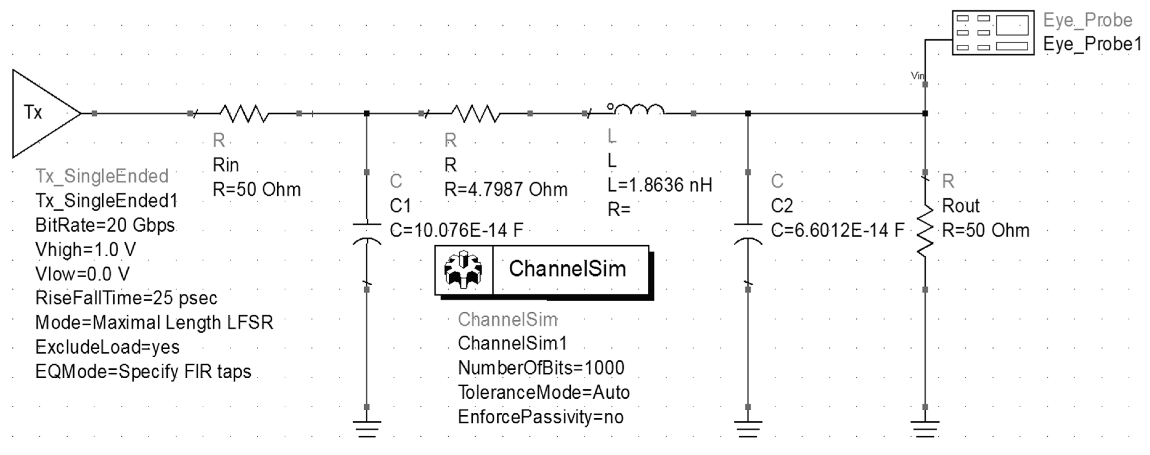
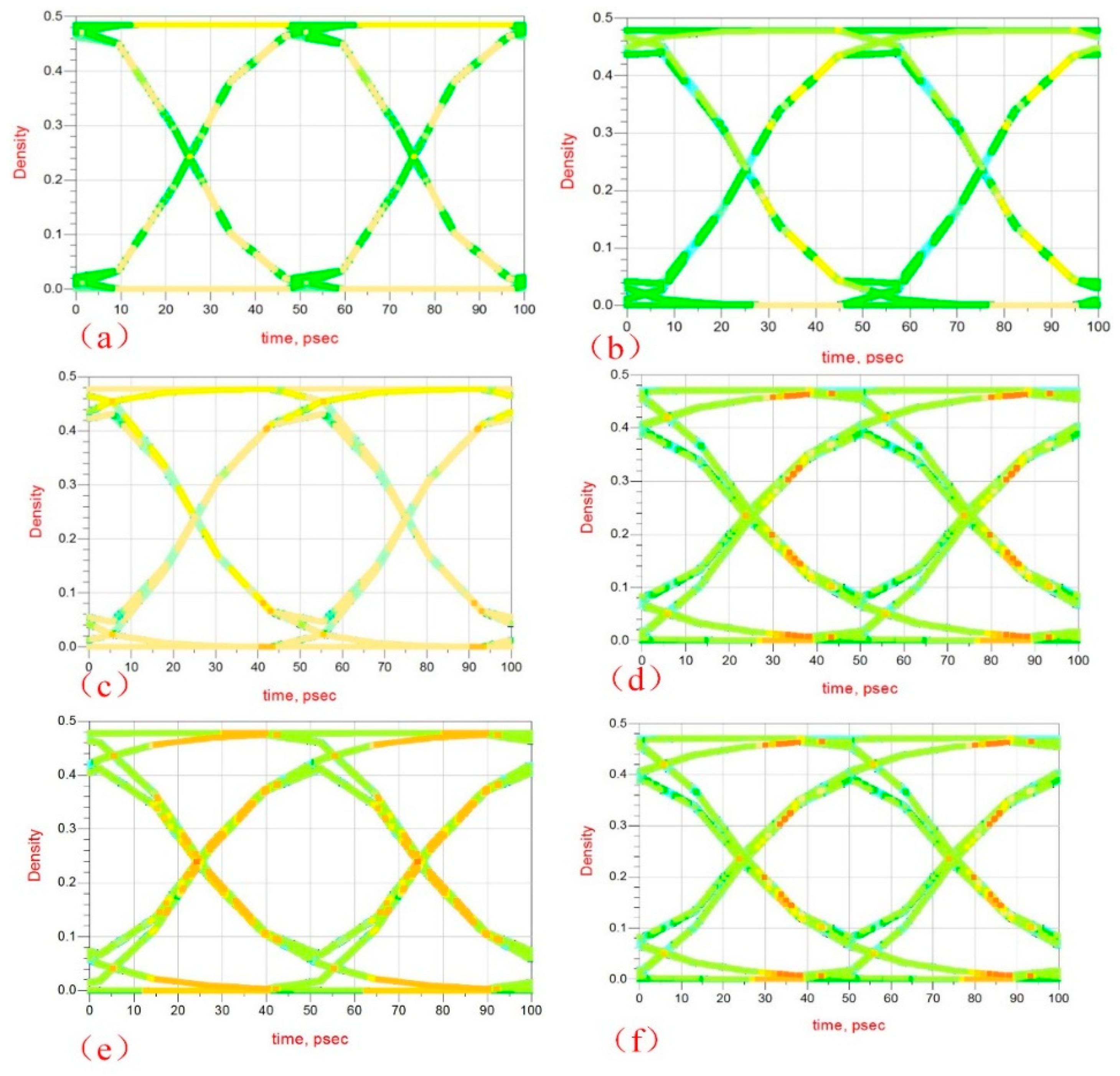
3.8. Eye Diagram Analysis

The eye diagram is a very successful and effective way of showing the quality and parametric information in digital transmission. Careful analysis of this visual display can give the user a first-order approximation of signal-to-noise, clock timing jitter and skew.
SP12 bonding wire (H1 = 250 μm, H2 = 254 μm, d = 25 μm) were selected as an illustration. In order to control variables, H2 is constant in this part. The span scanning ranged from 2000 μm to 4500 μm. In addition, the interval was 500 μm: 2000 μm, 2500 μm, 3000 μm, 3500 μm, 4000 μm and 4500 μm. Meanwhile, L1 varied from different span According to the schematic in Figure 15, the excitation signal was added at the input port as follows, the high level was 1 V, the low level was 0 V, the rising and falling time was set to 50 ps, and the bit rate of the signal was 10 Gbps. In this part, it recognizes a high level to be a logic 1 and a low level as a logic 0. The voltage values of logic 0 and logic 1, eye height and eye width in the eye diagram are shown in Table 8.
As illustrated in Table 8, with the increase of span, logic 1 voltage decreases, logic 0 voltage increases, and this will cause signal inconsistency between the input port and the output port and the increase of the bit error rate. Furthermore, as shown in Figure 16, the problem of unclear trace was aggravated with the increase of span, which will led to inter-symbol interference.

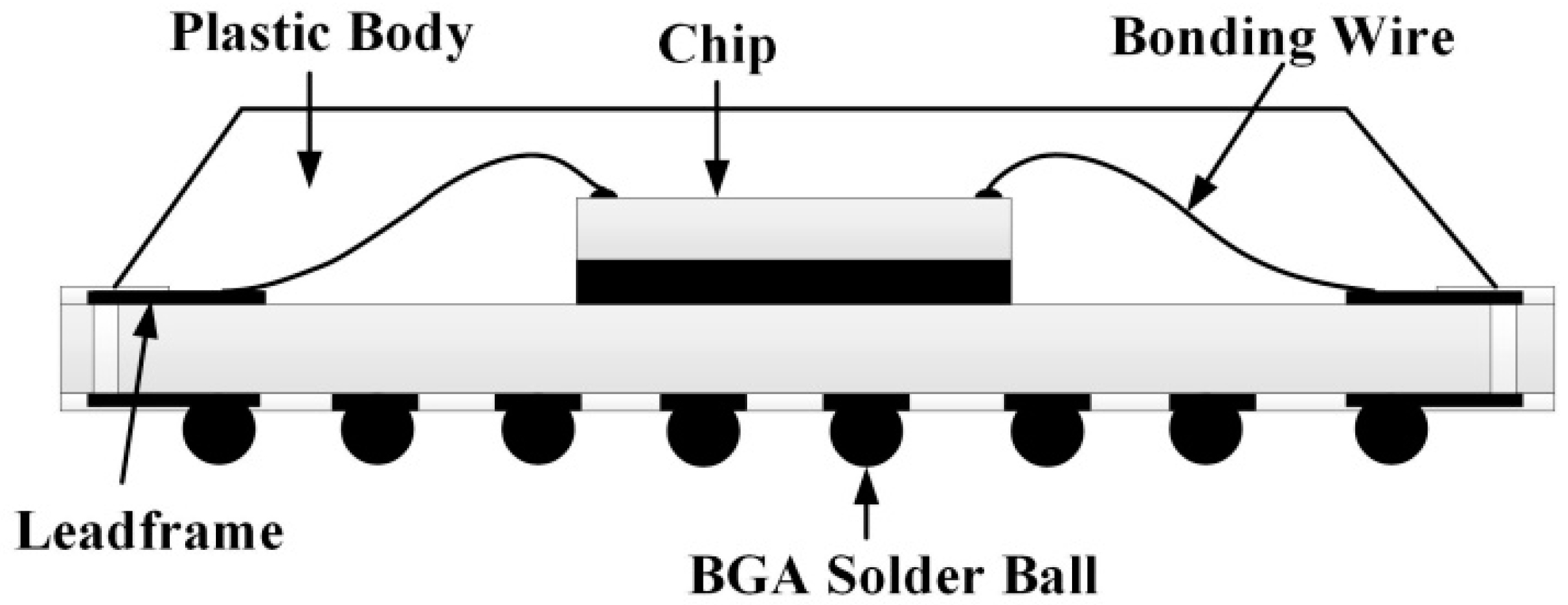
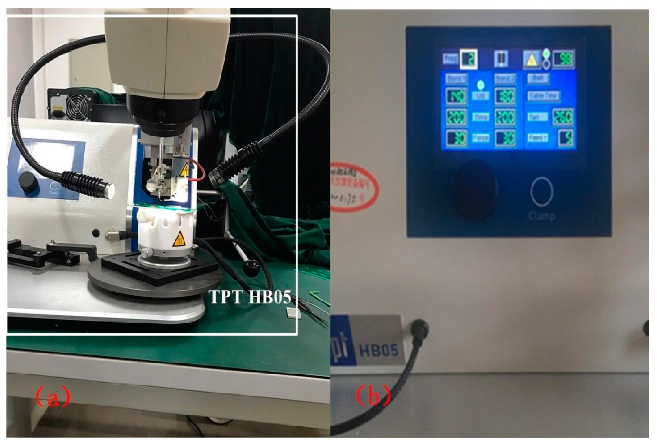
4. Bonding Wire Design and Measurement Experiment

In order to improve the correctness of the bonding wire simulation model, the bonding wire measurement experiments were designed in this section. The TPT HB05 type manual bonding machine was used to bond the gold wire in the test board. In addition, the vector network analyzer (VNA) was used to measure the bonding wire S parameter in the experiment. At the same time, based on the network port extension and port embedding theory, the S parameters of the device under test (DUT) were derived. With the error analysis, the results were compared with the original measurement data, which proves the correctness of the simulation results and design rules.

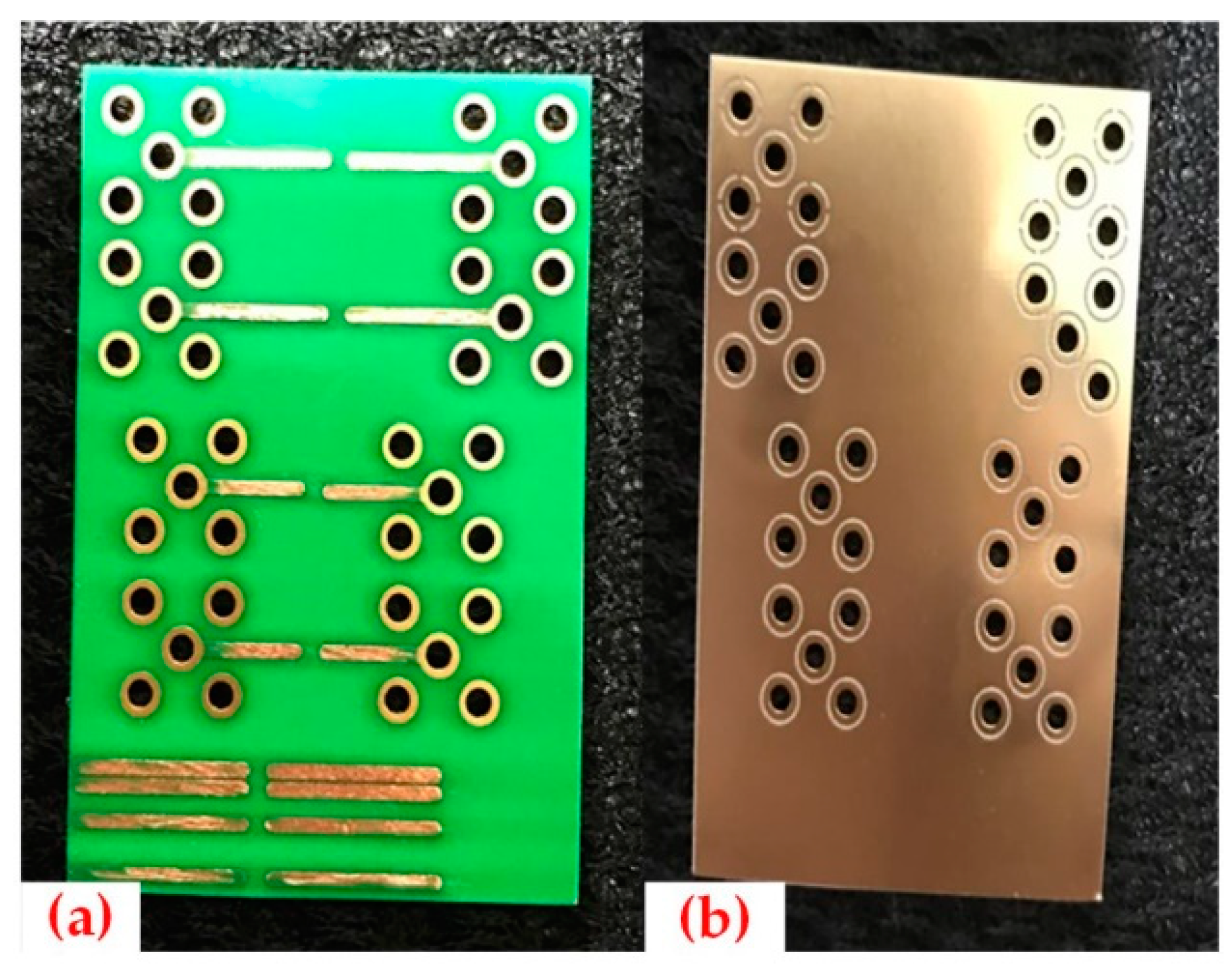
4.1. Circuit Board Design

In order to reduce the measurement error, it is necessary to shorten the length of the microstrip line and make the impedance matching design. Since the measurement frequency band had reached the GHz level, a Rogers RO4350B high-speed plate was chosen as substrate in accordance with simulation model. The test board length and width were 3.5 cm × 5.0 cm.
By using the empirical formula of the characteristic impedance for microstrip line, the approximate calculation of characteristic impedance is [20]:
Z 0 = 87 ε r + 1.41 ln ( 5.98 H 0.8 W + T )
In Equation (1), Z0 is the characteristic impedance of the microstrip line. As shown in Equation (1), εr is the dielectric constant of the substrate, H is the thickness of the substrate, W is the width of the microstrip line, and the T is the thickness of the microstrip line. The test board was connected with the VNA using the SMA connector. In order to weld with the SMA joint and shorten the microstrip line, the microstrip line length L was designed as 8 mm. The plate thickness H was 0.508 mm. A Rogers RO4350B was selected as double-layer plate with a dielectric constant of 3.48. Keeping the Z0 as constant 50 Ω based on Equation (1) and Cadence two-dimensional field solver impedance design tool, the rest of design parameters are obtained after adjustment: microstrip width W is 0.85 mm, thickness T is 0.05 mm. The specific microstrip line design parameters are as shown in Figure 17.
A TPT HB05 type semi-automatic bonding machine works on the basis of thermal compress bonding method. High pressure and high temperature caused metal plastic deformation in the bonding region, which realized the connection between the pad and the lead. Therefore, the hot pressing bonding method needs the hot pressing area to adopt the same metallurgy material, so that the hot pressing bonding process can be completed. The conventional PCB technique is not suitable for the bonding. This means that depositing Sn on copper pads as tin does not make the wire pressing successful. Considering about the bonding machine hot press temperature, hot press reliability and cost, bare gold process is the final choice for the microstrip line. There is no solder layer on the line, while the back of circuit board is deposited with gold as well as ground plane. Finally, the front and back of the test board are shown in Figure 18a,b.

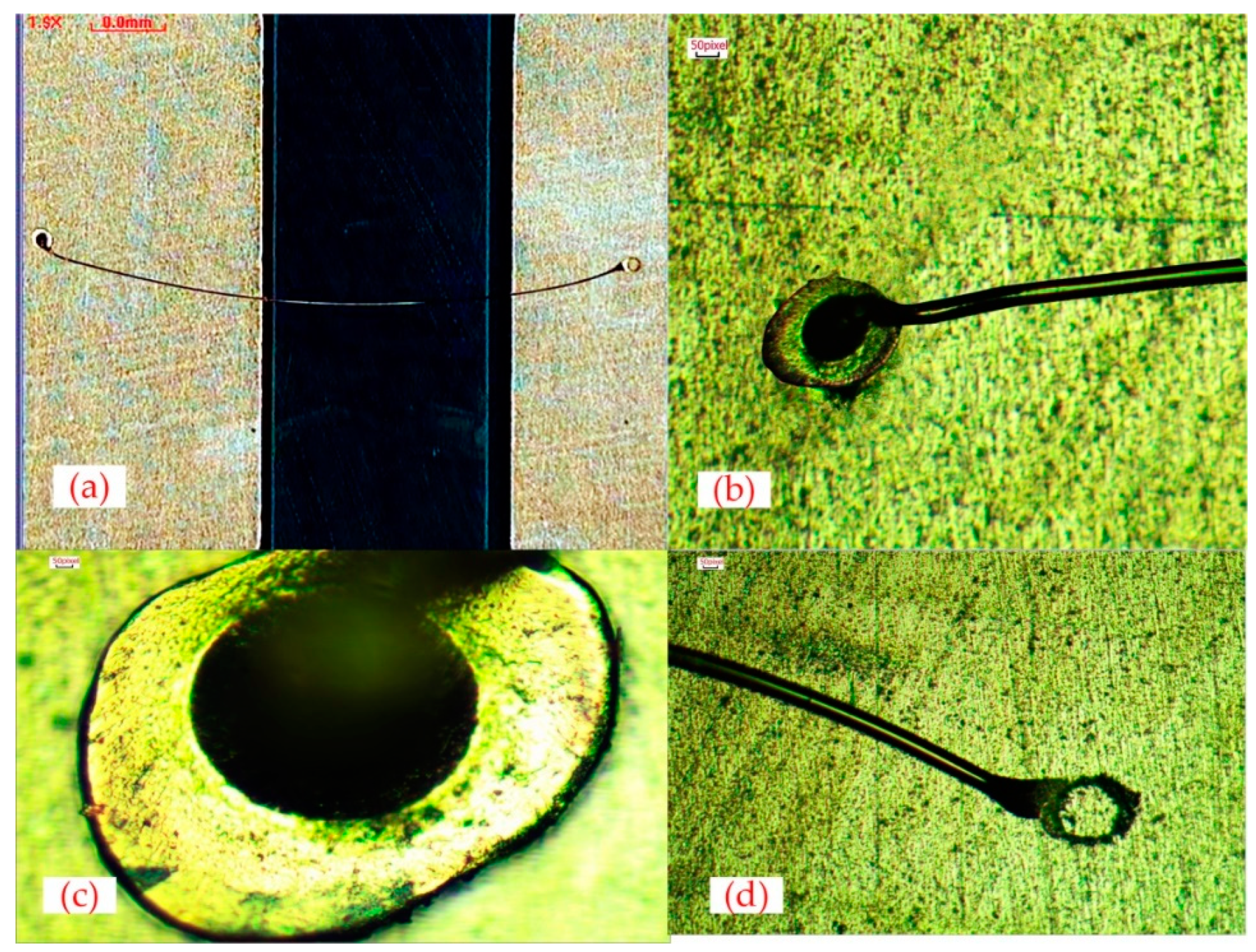
4.2. Bonding Wire Shape

The semi-automatic bonding machine (TPT HB05 type) was used to bond on the surface of a gold plated microstrip line. After adjusting the bonding parameters, the bonding wire under the requirements of the ball pad was finally obtained. The TPT HB05 bonding machine and bonding parameter settings are shown in Figure 19a,b.
The observation of bonding wire under video meter system (VMS) is shown in Figure 20a. The span was 4480 μm by measurement. To make sure there was no false welding, the first and second bonding point were checked through a microscope. The first and second bonding point of the bonding wire under the metallographic microscope is shown from Figure 20b–d.

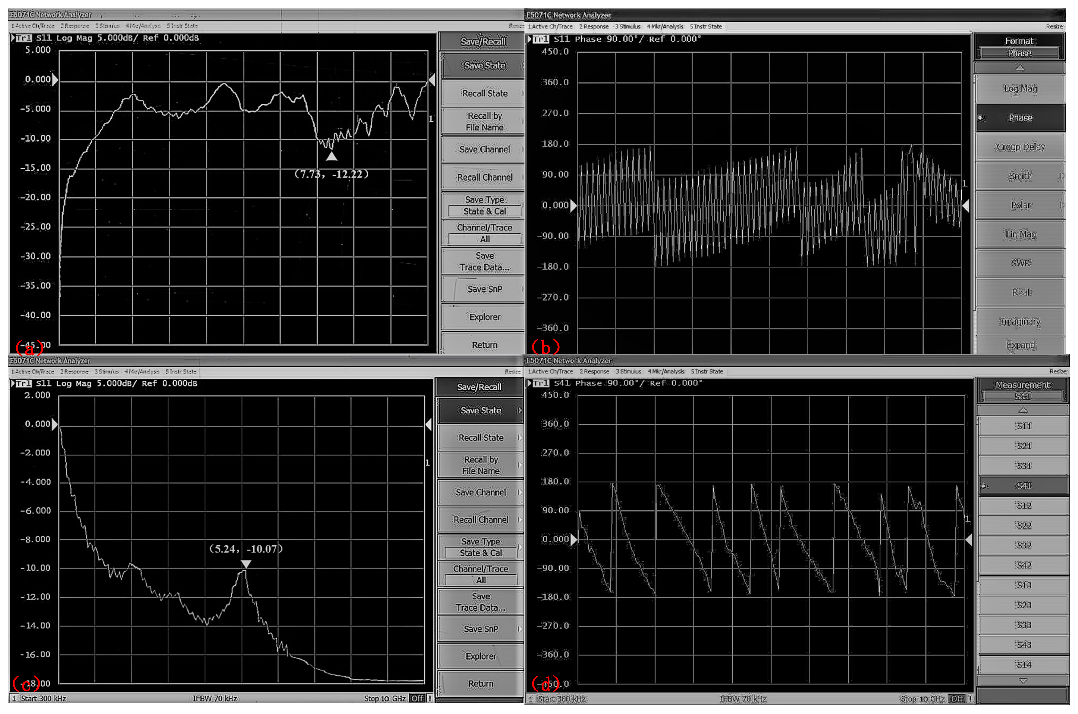
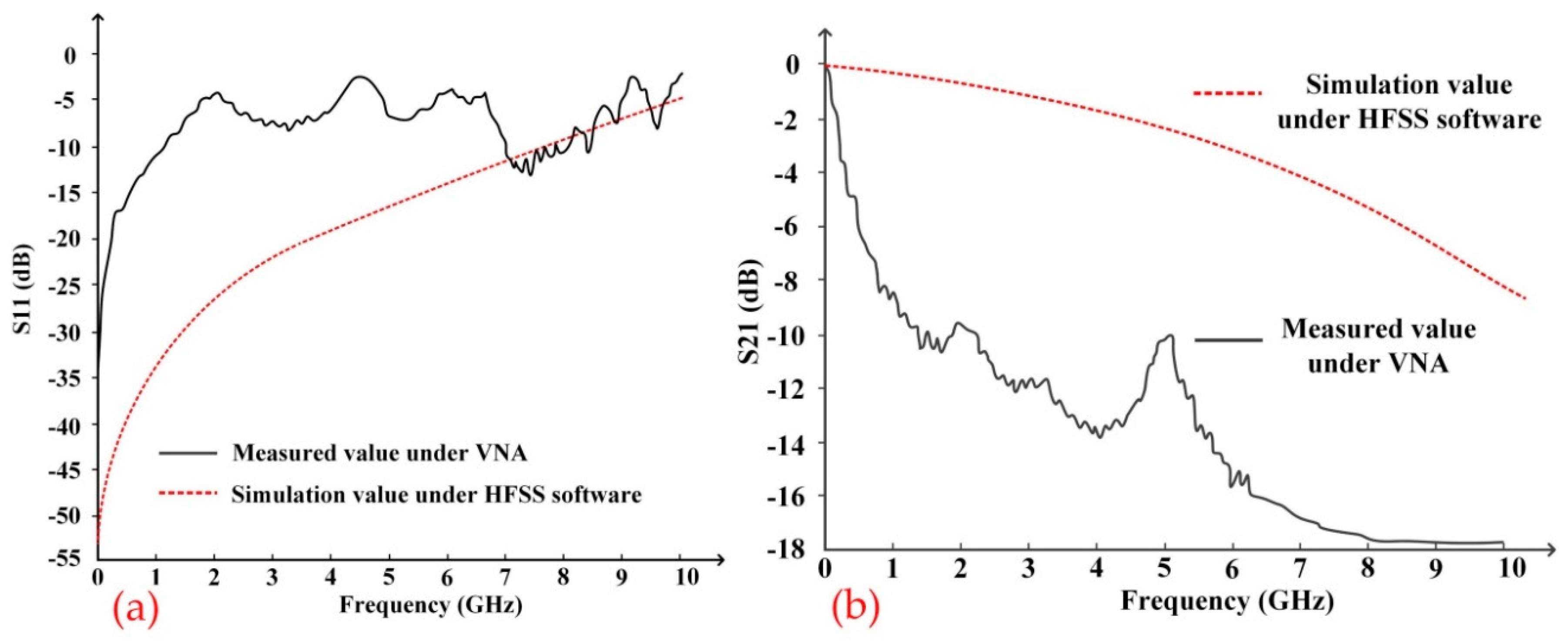
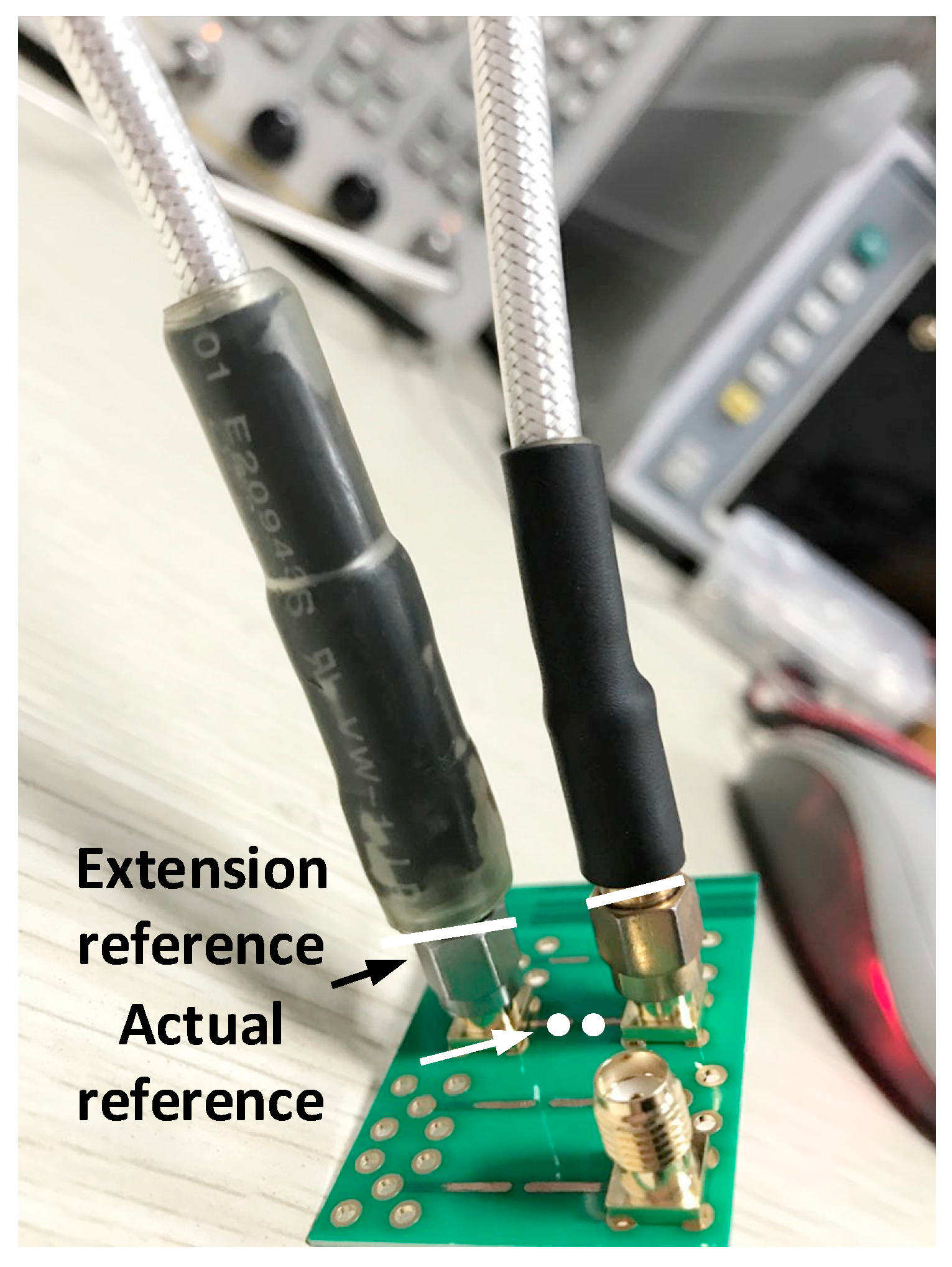
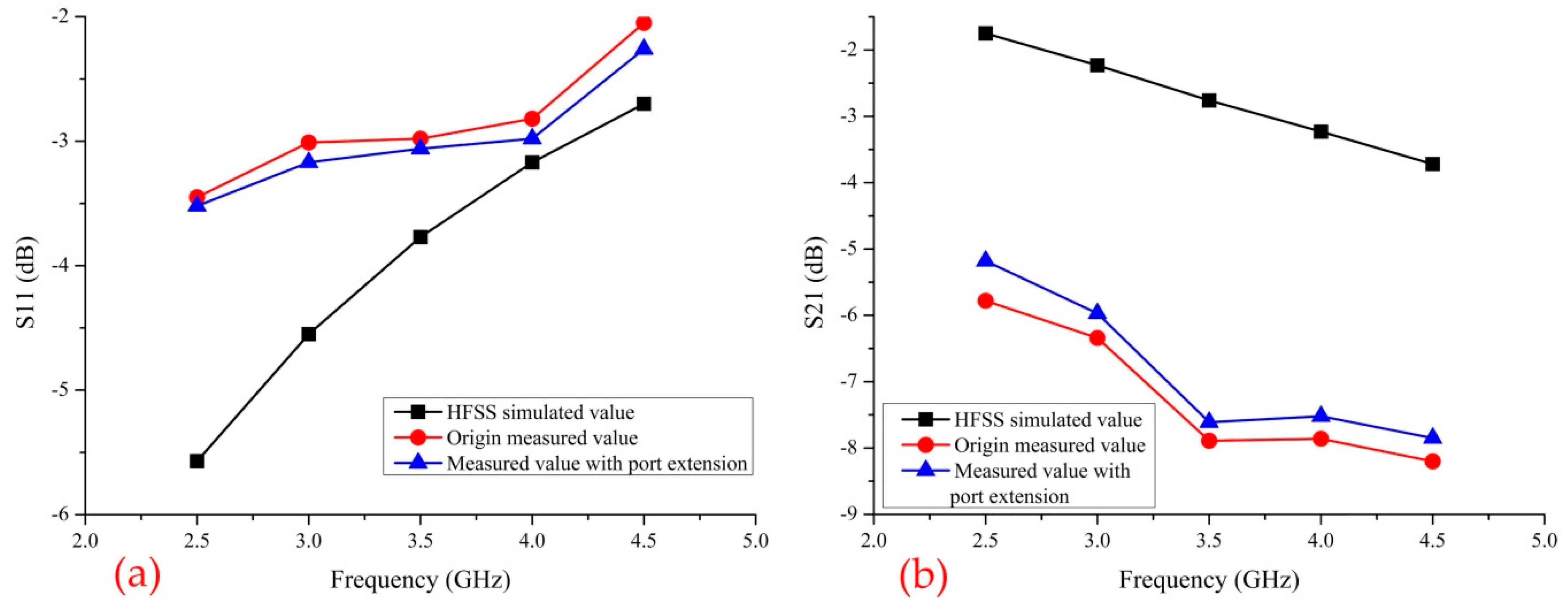
4.3. S Parameter Measurement And Error Analysis
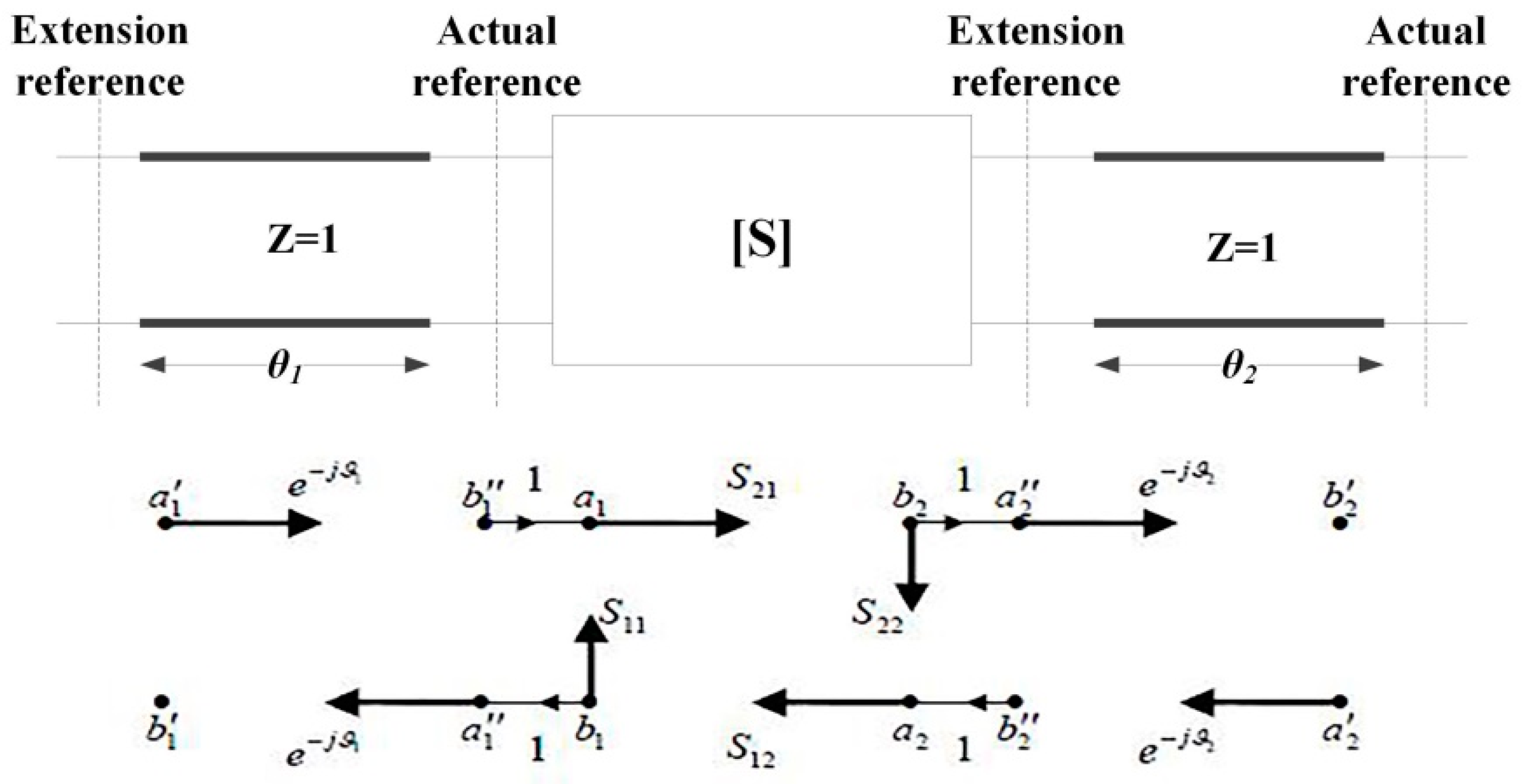
The measurement band is determined from 0.3 MHz to 10 GHz using VNA. The test board was connected to the instrument through SMA. Also, the S parameters of the device were measured after calibration. The S11, ϑ11, S21 and ϑ21 measured graphs of bonding wire are shown from Figure 21a–d. The measured data were compared with the simulation data (as shown in Figure 22).
It can be seen from Figure 22 that the trend of simulation curve and measured curve are consistent, that is, the S11 increases and S21 decreases with the rise of the frequency. This means that the signal reflection increases and the passing signal drops. The peak value of the test curve may appear because of the resonance problem of the whole test system. However, there is a certain gap between the measured value and the simulation value. The maximum error was about −20 dB in S11 curve, while −7 dB in S21 curve. The error comes mainly from the following three aspects:
1. Systematic error of measurement experiment
Due to the use of the SMA connector, the error of the measurement system is introduced to complete the measurement such as SMA conversion error, reflection/transmission measurement circuit error and fixture embedded error, as well as the random error in measurement.
2. Model error
For example, the simulation model is not precise enough resulting in less accurate modeling of the first and second bonding point; unable to establish completely accurate bonding wire model of actual experiment wire; the excitation port of stimulation is inconsistent with the actual measurement port.
3. Manufacturing error
The dielectric constant of the test plate is not constant resulting in dielectric loss; the actual impedance is inconsistent with calculation causing impedance mismatch and reflection loss problem.

4.4. Port Extension

Based on network analysis theory, the measured S parameters will inevitably have a fixture effect because the measured parameter is a joint cascading result with DUT and the fixture. The port extension is to move the position of the calibration reference and compensate the transmission line loss by measuring the electrical delay and loss for each single port. That is to say, the fixture is equivalent to a lossless transmission line (or lossy transmission line) under certain conditions. The measurement method is also used to measure the loss and phase shift of the transmission line. Finally, the reference surface is extended to the actual device to reduce the influence of the fixture on the final measuring results. The extension reference and actual reference in test are shown in Figure 23.
Based on the RF network theory:
[ b 1 b 2 ] = [ S ] o r i g i n [ a 1 a 2 ] = [ S 11 S 12 S 21 S 22 ] [ a 1 a 2 ]
[ b 1 b 2 ] = [ S ] e x t e n s i o n [ a 1 a 2 ] = [ S 11 S 12 S 21 S 22 ] [ a 1 a 2 ]
From the signal flow graph in Figure 24, the relationship between normalized reflection wave and incident wave is as follows:
[ a 1 a 2 ] = [ a 1 e j ϑ 1 a 2 e j ϑ 2 ] = [ e j ϑ 1 0 0 e j ϑ 2 ] [ a 1 a 2 ]
[ b 1 b 2 ] = [ b 1 e j ϑ 1 b 2 e j ϑ 2 ] = [ e j ϑ 1 0 0 e j ϑ 2 ] [ b 1 b 2 ]
According to the relationship among the parameters, the scattering matrix of extended surface [S] extension can be obtained after the calculation:
[ b 1 b 2 ] = [ b 1 e j ϑ 1 b 2 e j ϑ 2 ] = [ e j ϑ 1 0 0 e j ϑ 2 ] [ b 1 b 2 ] = [ e j ϑ 1 0 0 e j ϑ 2 ] [ S 11 S 12 S 21 S 22 ] [ a 1 a 2 ] = [ e j ϑ 1 0 0 e j ϑ 2 ] [ S 11 S 12 S 21 S 22 ] [ e j ϑ 1 0 0 e j ϑ 2 ] [ a 1 a 2 ]
[ S ] e x t e n t i o n = [ e j ϑ 1 0 0 e j ϑ 2 ] [ S 11 S 12 S 21 S 22 ] [ e j ϑ 1 0 0 e j ϑ 2 ] = [ S 11 e j 2 ϑ 1 S 12 e j ( ϑ 1 + ϑ 2 ) S 21 e j ( ϑ 1 + ϑ 2 ) S 22 e j 2 ϑ 2 ]
Taking the bonding wire with 4480 μm span as the example, the port extension and data analysis were performed at 2.5 GHz, 3.0 GHz, 3.5 GHz, 4.0 GHz and 4.5 GHz frequency points. After calibration of the VNA, the test circuit board was connected to Port 1, while Port 2 was kept empty. Then the reflection coefficient file was obtained. Furthermore, according to the cascade algorithm and signal flow chart, the port extension file was written in MATLAB. The S parameters of the final bonding wire are shown in the Table 9 after calculation.
The data of 5 fixed frequency points are calculated by extending the port, and the calculated data were compared with the result and original test data without error elimination using HFSS three-dimensional electromagnetic field simulation. The comparison graph of the three cases above is shown in Figure 25.
From the experimental data, system error can be eliminated to some extent by the port extension method making the measurement result more accurate. From the comparison between the simulation and the experimental data, the trends of S11 and S21 parameters were consistent. There was a deviation in some specific values, and the S parameter error contrast value was extracted in Table 10 among the five fixed points.
Due to limited experimental method and inability to establish the precise and accurate bonding wire loop model of experiment wire, even after port extension method and data processing, there was still some deviation between the simulation and measurement values. However, the experimental results have confirmed the results of S parameters simulation for the bonding wire and design rules. The error is also within the reasonable range. Therefore, the correctness of the simulation is proved.

5. Conclusions

This article adopted the method of electromagnetic field simulation analysis and actual experiment test. In addition, the electrical properties of gold bonding wire in WB package were studied. According to EIA/JEDEC97 standard, this paper establishes the electromagnetic structure model of gold bonding wire. The equivalent circuit model of bonding wire was proposed and discussed. The effect of bonding wire on signal transmission was analyzed by an eye diagram as well. Although it was difficult to obtain accurate mathematical relations between the electrical parameters and geometries and materials of bonding wire, the reasonable parameter select method and general rules can be obtained after qualitative analysis in this paper. The platform length, diameter, span, bonding height parameters and the influence of three kinds of loops on the S parameters of bonding wire were discussed. The results showed that: (1) the transmission performance of the bonding wire with high diameter, short span and arch height is good; (2) the flat length ratio only in a specific value, its signal transmission performance is good; (3) S-type arc signal transmission performance is the best, Q-type the second, M-type the worst. Furthermore, the design rules were derived from the simulation data. Meanwhile, based on RF circuit theory analysis and test method, gold bonding wire design and measurement experiments were implemented. The original measurement data was compared with the simulation model data and the error was analyzed. At last, the data of five frequency points were processed to eliminate the fixture error as much as possible based on port embedding theory. The measurement results using port extension method were compared with the original measurement data and electromagnetic field simulation data, which proves the correctness of the simulation results and design rules.

Author Contributions

W.T. guided other authors to complete this paper. He also supplied the latest supporting material. H.C. wrote the paper. W.Y. helped to revise the grammar of literature.

Acknowledgments

This work was supported by the National Natural Science Foundation of China (61176130), the Natural Science Foundation of Ningbo city of China (2016A610030).

Conflicts of Interest

The authors declare no conflict of interest.

References

  1. Fischer, A.C.; Korvink, J.G.; Roxhed, N. Unconventional applications of wire bonding create opportunities for microsystem integration. J. Micromechan. Microeng. 2013, 23, 905–923. [Google Scholar] [CrossRef]
  2. Chao, Y.Q.; Yang, Z.J.; Qiao, H.L. Progress on Technology of Wire Bonding. J. Electron. Process Technol. 2007, 4, 205–210. [Google Scholar]
  3. Tian, W. Electronic Packaging, Microelectromechanical and Micro System; Xidian University Press: Xi’an, China, 2012; Volume 1, pp. 59–66. [Google Scholar]
  4. Casper, T. Electrothermal simulation of bonding wire degradation under uncertain geometries. In Proceedings of the Automation & Test in Europe Conference & Exhibition, Dresden, Germany, 14–18 March 2016. [Google Scholar]
  5. Manoharan, S.; Patel, C.; Mccluskey, P.; Pecht, M. Effective decapsulation of copper wire-bonded microelectronic devices for reliability assessment. Microelectron. Reliab. 2018, 84, 197–207. [Google Scholar] [CrossRef]
  6. Ke, M.; Li, D.; Dai, X.; Jiang, H.; Deviny, I.; Luo, H.; Liu, G. Improved surge current capability of power diode with copper metallization and heavy copper wire bonding. In Proceedings of the IEEE European Conference on Power Electronics & Applications, Karlsruhe, Germany, 5–9 September 2016. [Google Scholar]
  7. Lorenz, G.; Naumann, F.; Mittag, M.; Petzold, M. In Mechanical characterization of bond wire materials in electronic devices at elevated temperatures. In Proceedings of the IEEE 5th Electronics System-integration Technology Conference (ESTC), Helsinki, Finland, 16–18 September 2014; pp. 1–6. [Google Scholar]
  8. Zhong, Z.W. Overview of wire bonding using copper wire or insulated wire. Microelectron. Reliab. 2011, 51, 4–12. [Google Scholar] [CrossRef]
  9. Liu, P.; Tong, L.; Wang, J.; Shi, L.; Tang, H. Challenges and developments of copper wire bonding technology. Microelectron. Reliab. 2012, 52, 1092–1098. [Google Scholar] [CrossRef]
  10. Ndip, I.; Huhn, M.; Brandenburger, F.; Ehrhardt, C.; Schneider-Ramelow, M.; Reichl, H.; Lang, K.D.; Henke, H. Experimental verification and analysis of analytical model of the shape of bond wire antennas. Electron. Lett. 2017, 53, 906–908. [Google Scholar] [CrossRef]
  11. Zuo, P.; Wang, M.; Li, H.; Song, T.; Liu, J.; Li, E.P. Modeling and analysis of transmission performance of bonding wire interconnection. In Proceedings of the IEEE MTT-S International Conference on Numerical Electromagnetic & Multiphysics Modeling & Optimization, Beijing, China, 27–29 July 2016. [Google Scholar]
  12. Yu, X.Q.; Bai, Y.D.; Zhou, Y.; Bai, W.; Yang, L.; Min, J.X. In EMI study of high-speed IC package based on pin map. In Proceedings of the IEEE Asia-Pacific International Symposium on Electromagnetic Compatibility, New York, NY, USA, 21–24 May 2012; pp. 305–308. [Google Scholar]
  13. Huang, N.K.H.; Jiang, L.J.; Yu, H.C.; Li, G.; Xu, S.; Ren, H.S. Fundamental components of the IC packaging electromagnetic interference (EMI) analysis. In Proceedings of the IEEE 21st Conference on Electrical Performance of Electronic Packaging and Systems, New York, NY, USA, 21–24 October 2012; pp. 141–144. [Google Scholar]
  14. Lim, J.H.; Kwon, D.H.; Rieh, J.S.; Kim, S.W.; Hwang, S.W. RF characterization and modeling of various wire bond transitions. IEEE Trans. Adv. Packag. 2005, 28, 772–778. [Google Scholar]
  15. Radojcic, R.; Chandrasekaran, A.; Lane, R. Hybrid Package Construction with Wire Bond and through Silicon Vias. U.S. Patent No. 8,803,305, 12 August 2014. [Google Scholar]
  16. Zhang, Y. Study on Influence of Grounding Vias Substrate on Performance of Millimeter Wave Products. J. Radio Eng. 2017, 47, 60–63. [Google Scholar]
  17. Lu, F.; Cao, Y.; Lian, B. Study on the electrical performance of one differential pair bonding fingers on different layers in wire bonding package. In Proceedings of the IEEE International Conference on Electronic Packaging Technology, Wuhan, China, 16–19 August 2016. [Google Scholar]
  18. Liang, Y.; Huang, C.; Wang, W. Modeling and characterization of the bonding-wire interconnection for microwave. In Proceedings of the IEEE MCM International Conference on Electronic Packaging Technology & High Density Packaging, Xi’an, China, 16–19 August 2010. [Google Scholar]
  19. Kung, H.K.; Chen, H.S.; Lu, M.C. The wire sag problem in wire bonding technology for semiconductor packaging. Microelectron. Reliab. 2013, 53, 288–296. [Google Scholar] [CrossRef]
  20. Liu, G.M. Dielectric Resonator Antenna Research. Master’s Thesis, Zhejiang University, Hangzhou, China, 2005. [Google Scholar]
Figure 1. Wire bonding (WB) package structure.
Electronics 08 00365 g001
Figure 2. S-loop wire geometric parameters.
Electronics 08 00365 g002
Figure 3. Single bonding wire simulation model.
Electronics 08 00365 g003
Figure 4. HFSS simulation model.
Electronics 08 00365 g004
Figure 5. Three S-loop wires with different flat lengths.
Electronics 08 00365 g005
Figure 6. (a) S11 of bonding wire with different flat length; (b) S21 of bonding wire with different flat length.
Electronics 08 00365 g006
Figure 7. (a) S11 of bonding wire with different diameter; (b) S21 of bonding wire with different diameter.
Electronics 08 00365 g007
Figure 8. (a) S11 of bonding wire with different span; (b) S21 of bonding wire with different span.
Electronics 08 00365 g008
Figure 9. (a) S11 of bonding wire with different bonding height; (b) S21 of bonding wire with bonding height.
Electronics 08 00365 g009
Figure 10. Bonding wire loop modes: (a) Q-loop bonding wire; (b) S-loop bonding wire; (c) M-loop bonding wire.
Electronics 08 00365 g010
Figure 11. (a) S11 of bonding wire with different loop modes; (b) S21 of bonding wire with loop modes.
Electronics 08 00365 g011
Figure 12. The SPICE equivalent circuit model of bonding wire.
Electronics 08 00365 g012
Figure 13. The equivalent impedance model of Z11.
Electronics 08 00365 g013
Figure 14. Comparison between SPICE and HFSS (a) S11; (b) S21.
Electronics 08 00365 g014
Figure 15. Eye diagram analysis schematic.
Electronics 08 00365 g015
Figure 16. Eye diagram with different span. (a) 2000 μm (b) 2500 μm (c) 3000 μm (d) 3500 μm (e) 4000 μm (f) 4500 μm.
Electronics 08 00365 g016
Figure 17. Microstrip line design parameters.
Electronics 08 00365 g017
Figure 18. Test circuit board: (a) front (b) back.
Electronics 08 00365 g018
Figure 19. (a)TPT HB05 bonding machine (b) Bonding parameter settings.
Electronics 08 00365 g019
Figure 20. (a) Bonding wire under VMS; (b) First bonding point under 10 times microscope; (c) First bonding point under 40 times microscope; (d) Second bonding point under 20 times microscope.
Electronics 08 00365 g020
Figure 21. (a) Measured S11 of circuit-under-test; (b) Measured ϑ11 of circuit-under-test; (c) Measured S21 of circuit-under-test; (d) Measured ϑ21 of circuit-under-test.
Electronics 08 00365 g021
Figure 22. Comparison between simulated and measured values: (a) S11; (b) S21.
Electronics 08 00365 g022
Figure 23. Extension reference and actual reference in test.
Electronics 08 00365 g023
Figure 24. Port extension outward and signal flow graph.
Electronics 08 00365 g024
Figure 25. Comparison of S parameters: (a) S11; (b) S21.
Electronics 08 00365 g025
Table 1. Model material parameters.
NameMaterialDielectric Constant
S-loop wireGold0.99996
MicrostripCopper0.99991
ChipSilicon11.9
SubstrateRogers RO4350B3.66
GroundCopper0.99991
Table 2. Comparison of S21 extremum under different flat length.
Ratio of Flat Length to SpanSP00SP12SP20SP40SP60SP70
Min S21 (Insertion Loss)/dB−9.10−8.71−9.34−9.58−9.82−9.92
Corresponding frequency/GHz17.6317.3817.5817.5817.4817.48
Passing signal/incoming signal/%35.0736.6934.1233.1932.2831.92
Table 3. Comparison of S21 extremum under different diameter.
Diameter/μm152025303540
Min S21 (Insertion Loss)/dB−9.42−8.87−8.71−8.55−8.37−8.16
Corresponding frequency/GHz17.5317.4317.3817.3817.3317.18
Passing signal/incoming signal/%33.8036.0136.6737.3838.1639.06
Table 4. Comparison of S21 extremum under different span.
Span/μm250030003500400045005000
Min S21 (Insertion Loss)/dB−8.01−8.37−8.69−8.71−8.96−9.03
Corresponding frequency/GHz25.1222.5419.8217.3315.6714.33
Passing signal/incoming signal/%39.7638.1536.7736.6935.6535.36
Table 5. Comparison of S21 extremum under different bonding height.
Bonding Height/μm210230250270290310
Min S21 (Insertion Loss)/dB−8.61−8.59−8.71−8.79−8.88−9.02
Corresponding frequency/GHz17.5817.3317.3817.2817.4317.38
Passing signal/incoming signal/%37.1137.2036.6936.3535.9735.40
Table 6. Comparison of S21 extremum under different loop modes.
Bonding Wire LoopMQS
Min S21 (Insertion Loss)/dB−9.59−9.29−8.71
Corresponding frequency/GHz17.7317.6817.38
Passing signal/incoming signal/%33.1534.3236.69
Table 7. The influence of WB parameters on electrical properties.
FactorsMeasurementRestriction
Flat Length
(S-loop wire)
Flat length changes nonlinearly with return loss and insertion loss.
The flat length only stands in a specific value, and its signal transmission performance is good
Through the comparison of the data, it is found that signal quality is the best when the flat ratio of length and span is 12%, maybe the best L1/L is 11% or 13% in real operation.
DiameterThe bigger diameter is, the better electrical properties are.
Insertion loss and equivalent inductance decline with increasing diameter.
Excessive increase in wire diameter:
1. Aggravate the cost of materials
2. Decline in toughness
SpanThe shorter loop span is, the better electrical properties are.
Shorter loop can reduce signal loss and improve the quality of signal transmission.
Too shorter span:
1. Increase line tension,
2. Make welding spot unstable
3. Cause wire sag and sweep problem
Bonding HeightThe lower wire height is, the better electrical properties are.Too lower height:
1. Stress concentration
2. Phenomenon of expanding under hot condition and shrinking under cold condition in bonded component.
Table 8. Eye diagram characteristics under different span.
NumberSpan/μmLogical 1 Voltage/VLogical 0 Voltage/VEye Height/VEye Width/ps
a20000.4730.0120.42450
b25000.4580.0210.39250
c30000.4500.0280.35149.5
d35000.4410.0320.32049.25
e40000.4400.0390.29448.75
f45000.4250.0460.26148
Table 9. Bonding wire S parameter results file DUT_WireBond.TXT.
Frequency/GHz | S 11 | ϑ 11 | S 21 | ϑ 21
2.56.67 × 10−1−2.51 × 105.51 × 10−23.27 × 10
3.06.94 × 10−15.87 × 105.03 × 10−2−4.62 × 10
3.57.03 × 10−12.60 × 1024.16 × 10−2−8.54 × 10
4.07.10 × 10−1−4.21 × 104.21 × 10−2−1.08 × 10
4.57.71 × 10−18.59 × 104.05 × 10−21.85 × 10²
Frequency/GHz | S 12 | ϑ 12 | S 22 | ϑ 22
2.54.65 × 10−23.24 × 106.89× 10−1−2.69 × 10
3.04.47 × 10−2−2.89 × 107.23 × 10−14.17 × 10
3.54.32 × 10−2−5.69 × 107.42 × 10−13.28× 10²
4.04.02 × 10−2−6.78 × 1027.38 × 10−1−8.26 × 10
4.53.65 × 10−21.95 × 1027.94 × 10−11.22 × 10
Table 10. Comparison between simulated and measured value with port extension.
S ParameterMax Relative ErrorFrequencyMin Relative ErrorFrequency
S1133%2.5 GHz11%4.0 GHz
S2169%3.5 GHz39%2.5 GHz

