Article

Full-Band Oversized Turnstile-Based Waveguide Four-Way Power Divider/Combiner for High-Power Applications

1
Department of Ingeniería de Comunicaciones, Edif. Ingeniería de Telecomunicación, Universidad de Cantabria, Plaza de la Ciencia s/n, 39005 Santander, Spain
2
Department of Ingegneria Elettronica, Universitá degli Studi di Roma Tor Vergata, Via del Politecnico, 1, 00133 Roma, Italy
*
Author to whom correspondence should be addressed.
Electronics 2019, 8(2), 193; https://doi.org/10.3390/electronics8020193
Submission received: 22 January 2019 / Revised: 31 January 2019 / Accepted: 6 February 2019 / Published: 7 February 2019
(This article belongs to the Section Microwave and Wireless Communications)

Abstract

:
Very high-power and high-efficiency microwave applications require waveguide structures to combine/divide the power from/to a variable number of high-power solid-state devices. In the literature, among the different waveguide configurations, those capable of providing the maximum output power show a limited relative bandwidth. To overcome this limitation, in this paper a full-band (40%) waveguide power divider/combiner specifically designed for high-power applications (up to several kW) is presented. The proposed structure uses an evolved turnstile junction with a standard rectangular waveguide common port, rotated 45°, with respect to its central axis, to divide/combine the signal to/from the four output/input rectangular ports. The inclusion of an oversized central cavity together with circular and rectangular waveguide impedance transformers at the common port allows the achievement of a full-band operation with excellent electrical performance, while maintaining a very simple and compact configuration. Only two layers of metal are required for the physical implementation of this structure in platelet configuration. A prototype has been designed covering the full Ka-band (26.5–40 GHz), showing an excellent measured performance with around 30 dB of return loss, 0.18 dB of insertion loss, and less than 1.5° of phase imbalance.

1. Introduction

Modern communication systems and radar applications demand wider and wider bandwidths, capable of allocating the increasing number of services and/or to cover larger frequency ranges to reduce costs and weights of the system by the minimization of transmitter/receiver hardware. On the other hand, high-power applications have benefited in recent years from the development of solid-state technologies, such as GaN (Gallium-Nitride) monolithic microwave integrated circuits (MMICs), each one with several watts of delivered power at microwave frequencies [1,2,3,4]. However, when the aimed application requires hundreds or even thousands of watts of delivered power, very low-loss power combining techniques in waveguide technology appears to be the only viable solution, which becomes more noticeable as the frequency enters in the microwave range.
Through the years, many different techniques have been developed for obtaining very high-power transmitters by combining the performance of a variable number of high-power solid-state devices. These techniques are based on dedicated structures capable of dividing/combining the input/output signal to/from those devices. Many works found in the literature propose the use of radial [5,6,7] or coaxial dividers/combiners, both in circular waveguide [8,9,10] and square waveguide [11,12]. They can be easily adapted to integrate a large number of high-power devices, while their bandwidth performance can be optimized from narrow to multi-octave bands, as well. However, they require coaxial input/output ports or coaxial sections within the structure for symmetric signal distribution. These coaxial parts represent a serious power handling capability limitation at high frequencies. For example, a 2.92 mm connector (K-connector) is typically limited to 20 W at 40 GHz [13]. Alternative structures, based on the same philosophy of distributing the amplification stages within a waveguide, but avoiding coaxial port [14,15], are inherently limited in the number and size of single amplifiers that can be hosted in the waveguide cavity, and consequently in the amount of the total power that can be obtained.
Other approaches exploit the traveling-wave concept [16,17,18,19] for the signal division and subsequent combination in order to collect enough power at the output port. These structures require a tight control of the amplitude and phase imbalances among the different stages to maintain a high efficiency. For this reason, practical implementations rarely achieve 30% of the fractional bandwidth. Classical N-port waveguide dividing networks, such as T-junctions, hybrid couplers, or magic-Ts [20,21,22,23], are cascaded in order to join the required number of individual power amplifiers in high-power applications. These structures may result in complicated or bulky arrangements. Finally, a group of works deal with five-port or six-port junctions in a turnstile-like configuration [24,25,26,27]. In these structures, the common port is a standard rectangular waveguide rotated 45° with respect to the junction axial axis. In this way, the signal is symmetrically distributed among the four rectangular ports of the junction, avoiding coaxial ports that seriously limit the power handling capability. When a sixth port is included [24,25], it can be connected to a matched load to further improve the isolation between the four accesses in the junction. These structures show some interesting characteristics, such as mechanical simplicity, compact size, and high-power handling capability, but the designs developed so far show a relative bandwidth below 30%. A general overview of such spatial power combining techniques can be found in [28].
In this paper, we propose an evolved turnstile-based four-way power divider/combiner that notably extends the usable bandwidth up to a waveguide full-band coverage (40% relative bandwidth), while it maintains a very simple and compact structure, very suitable for high-power applications (several kW). In order to accomplish the improved bandwidth, an oversized junction cavity and two short matching steps, in circular and rectangular waveguides, at the common port are included in the structure. These variations, together with a two-step central matching element (scatterer), provide the additional flexibility required for the bandwidth widening with excellent electrical performance. The structure is completed with E-plane bends that enable the measurement of the system in an in-line configuration, facilitating the integration with external power amplifiers. Special care has been taken for simplifying the mechanical production through the implementation in platelet configuration, with only two metal layers, and using standard computer numerical control (CNC) milling techniques.
Section 2 details the design of the two main parts in the circuit—the junction and the E-plane bends—and provides simulation results of the whole structure. Power handling capability considerations are given in Section 3, whereas power combiner/divider full characterization and results are shown in Section 4. Finally, Section 5 presents some conclusions.

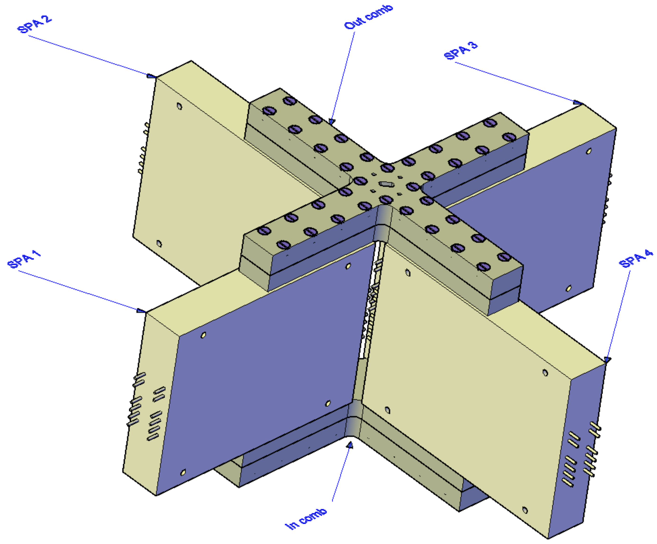
2. Power Divider/Combiner Design
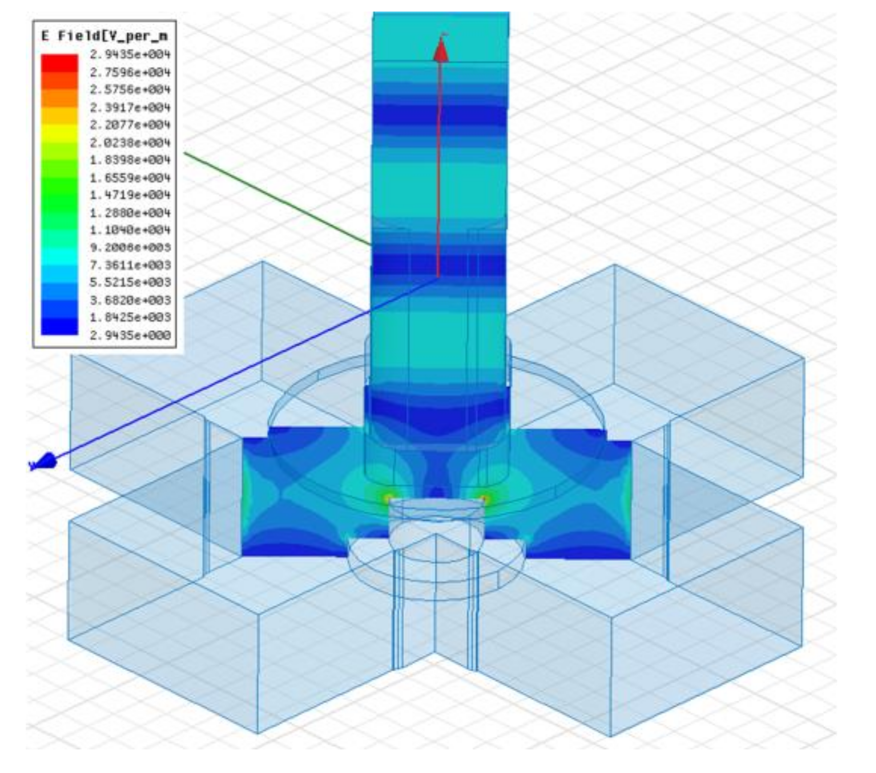
The design of the power divider/combiner, intended to cover the full Ka-band (26.5–40 GHz), was divided into two main parts that were designed independently: the turnstile-based junction and the E-plane bend. Since the structure can be used interchangeably as a power divider or combiner, in the following it will be explained as a divider, with a common input port and four output ports.

2.1. The Junction

A 3D sketch of the proposed junction is presented in Figure 1, while top and side views are shown in Figure 2, together with the definition of the design parameters. The design was started with the classical turnstile junction, which can easily achieve full-band performance [29] or even an octave bandwidth in combination with reduced-height waveguides [30]. Main guidelines to design a turnstile junction can be found in [31]. However, the circular waveguide common port would require a transition to coaxial waveguide for signal feeding which, as commented before, need to be avoided due to its inherent power handling capability limitation. For this purpose, an alternative feeding technique was adopted, based on a rectangular waveguide rotated 45°, with respect to the junction axial axis, that symmetrically distributes the input signal among the output ports [24,25,26,27]. This solution, together with the use of full-height waveguides, assured the maximum power handling capability of the structure.
Unfortunately, and as a consequence of this modification, the bandwidth of the junction was reduced to a great extent [24,25,26,27], making necessary the inclusion of additional sections that broaden the usable frequency range with good electrical performance. In order to overcome these bandwidth limitations, this work proposes the use of an oversized cavity in the junction by using an impedance transformer defined by parameters acav and lcav, shown in Figure 2, which was machined with a milling tool radius of 0.5 mm. This modification by itself enabled the achievement of the desired bandwidth, but care has to be taken with parameter acav because, if it is made very large, higher-order modes appear in the junction, limiting its operational bandwidth. Therefore, acav was defined between the standard waveguide width value, a, and the waveguide width value that produced a cutoff frequency for the first higher-order mode, TE20, at the desired frequency upper limit. Precise values for acav and lcav were obtained by post-optimization techniques. Once the oversized cavity main dimensions were defined, this structure had to be conveniently matched to the rectangular common port. Firstly, a circular waveguide matching step, defined by parameters dcir and lcir, was included. This circular section was advisable due to the circular symmetry of the cavity and the scatterer, providing a smooth transition from an electromagnetic point of view. The initial value for parameter dcir was calculated so that the cutoff frequency of the first propagated mode in this circular section, TE11, was close to the cutoff frequency of mode TE10, defined by acav. Again, dcir and lcir final values were obtained by post-optimization. And secondly, a rectangular waveguide impedance transformer, defined by parameters arec, brec, and lrec, was introduced in this junction to adapt the previous circular waveguide section to the rectangular waveguide common port. Thus, the performance goal of 40% of relative bandwidth with 30 dB of return loss could be obtained. The milling tool radius in this rectangular transformer was 0.8 mm. Finally, a section with WR28 nominal dimensions and length l0 provided a suitable interface for the connection of the input signal. This last section was designed to be machined with a 1-mm-radius milling tool.
The design and optimization of this structure was carried out with a mode-matching (MM) software, such as µWave Wizard from MICIAN, and later checked with a full 3D electromagnetic simulator, such as ANSYS HFSS. The design parameters final values are presented in Table 1, while the simulated results are shown in Figure 3.
From Figure 3, the return loss at common port was better than 30 dB in the whole 26.5–40 GHz frequency range, whereas the transmission between the input port and any of the output ports met the theoretical value of −6.02 dB. The simulated results showed a large improvement with respect to state-of-the-art turnstile-based power dividers.

2.2. E-Plane Bend

The structure proposed in this work was intended to be integrated with four external power amplifiers [32] in a future application. For this purpose, a first unit was adopted to divide the input signal among the four amplifiers and then, a second unit, recombined their outputs for obtaining a very high-power amplification stage. For this reason, the output ports needed to be arranged in an in-line configuration with respect to the input port. Therefore, E-plane bends needed to be placed following the junction output ports.
The design of the bends was performed accounting for the mechanical process required for their physical realization. Since the structure was implemented in a platelet configuration, the bend corners had to be rounded accordingly. This imposed some limitations in the bend shape and performance. A sketch of the designed bend is depicted in Figure 4, together with its design parameters.
The goal of the bend design was a return loss around 40 dB for the whole frequency range, which made this part nearly transparent for the junction from the electromagnetic point of view. The bandwidth of these classes of bends mainly depend on the number of steps. For our application, with the desired full-band coverage, it was found necessary to use a three-step bend, as shown in Figure 4. The effect of rounded corners was important in this type of bends as well as the transition between the rounded WR28 waveguide, mechanized in Layer 1, and the standard WR28 waveguide, not included in the structure but present when connected to the power amplifier. The best values for the design parameters were obtained by optimization and are included in Table 2. The simulated reflection results are plotted in Figure 5, whereby values near −40 dB can be observed.

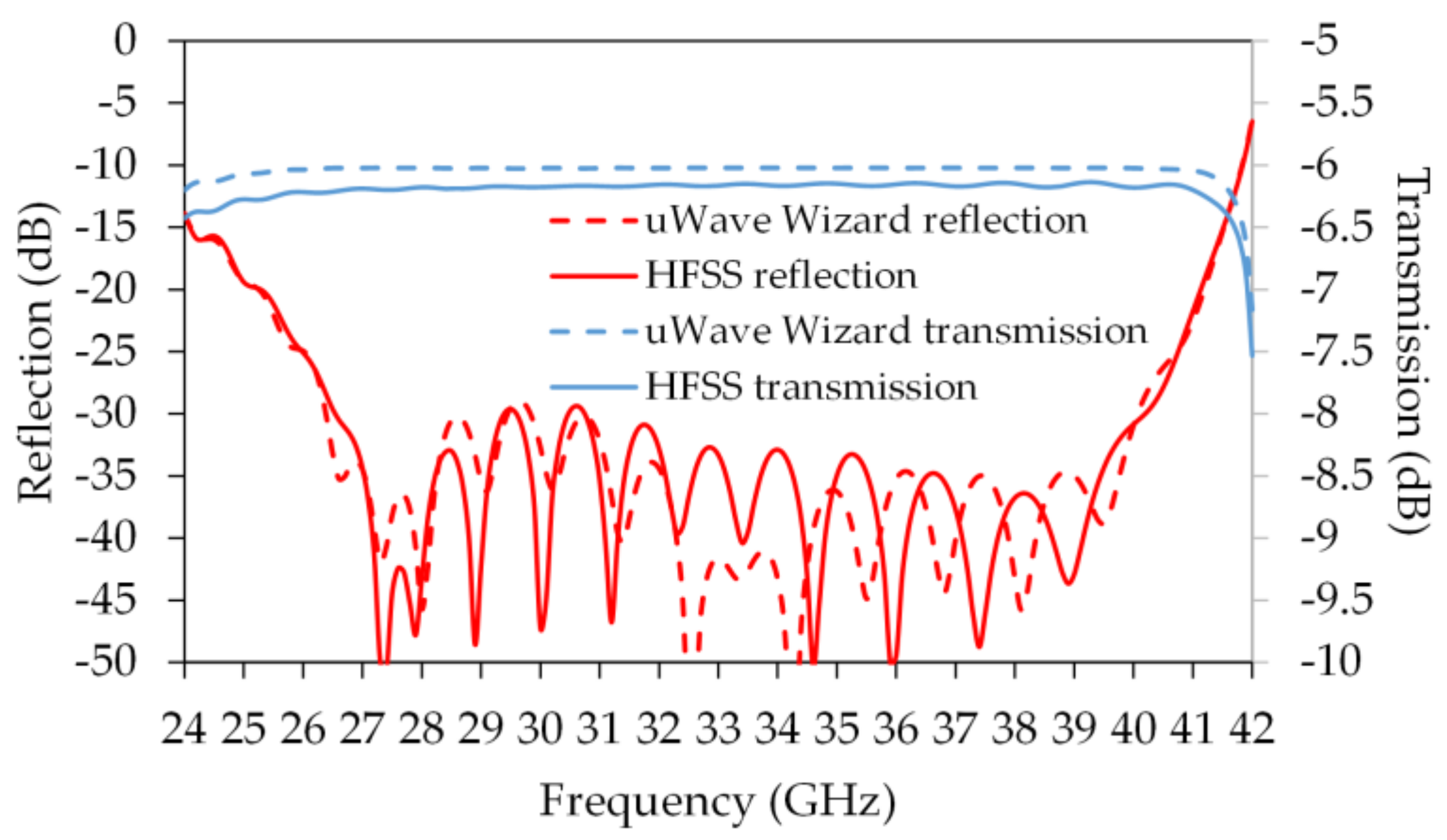
2.3. Full Structure Simulation

The proposed junction was connected to the E-plane bends through straight waveguide sections in such a way that the distance between two opposite output ports was exactly 170 mm, which is the distance set for the future application. Nevertheless, the power divider could be made much more compact if needed, with similar electrical performance. The whole structure is shown in Figure 6 as implemented in HFSS, whereas the simulated results are plotted in Figure 7.
In order to account for the insertion loss between input port and all the output ports in the simulation, a finite conductivity boundary condition was applied to the structure in Figure 6. The electrical conductivity used in this simulation was the theoretical value corresponding to the aluminum (i.e., σ = 3.8 × 10⁷ S/m). From the results, the mean value of insertion loss across the band was 6.17 dB, that was 0.15 dB of additional loss produced by the ohmic resistance. This value was clearly dominated by the long straight waveguide branches. The difference between the insertion loss curves simulated with the two CAD (Computer Aided Design) tools, shown in Figure 7, was due to not applying the finite conductivity value to the µWave Wizard simulation.
As can be observed in Figure 7, the reflection traces followed the curves of the stand-alone junction in Figure 3, with values of −30 dB in the bandwidth, demonstrating that bends were nearly transparent. The minor reflections between parts that travelled through the long waveguide straight sections produced the ripples in the curves.

3. Power Handling Capability Estimation

The designed power divider is intended for high-power applications and; therefore, it has to withstand hundreds of watts. In order to assure its operation under such conditions, an estimation of its power handling capability was carried out with simulation tools.
The junction, which is the most sensitive circuit element in terms of power handling capabilities, due to its reduced dimensions and sharp edges, was simulated in HFSS to obtain the maximum electric field within the structure. Taking into consideration that the air breakdown at sea level is 3 × 10⁶ V/m and the obtained maximum electric field was 2.4 × 10⁴ V/m at 40 GHz for 1 W input power, as shown in Figure 8 then, theoretically, the maximum power handled by the divider, before breakdown, could be calculated as (1).
Pmax = (Ebrk/Emax)2 = 10.3 kW
Notwithstanding the previous value, typical safety factors recommend the use of the circuit at 50% or even 25% of the maximum power, thus more than 5 kW or 2.5 kW respectively.
Such high-power that this device could handle would produce a noticeable temperature rise in the structure, even though it shows minor insertion loss. Since the power divider was completely machined in aluminum, it can be easily attached to a radiating element that boosts the heat dissipation.
The design of this combiner was made with the aim of using four spatial power amplifiers (SPAs), each one providing nearly 50 W of output power in the 32–38 GHz band, using 16 gallium-arsenide (GaAs) MMICs [32]. A representation of the complete assembled high-power amplifier (HPA) is shown in Figure 9. For simplicity of view, Figure 9 does not show heat sink and cabling of each SPA.
Still higher RF power could be reached by the amplifier, in Figure 9, using the GaN technology, now easily available from many foundries [33,34,35,36]. Reliability for GaN is today a well assessed process [37,38,39], also considering particular designs in temperature [40]. GaN MMIC HPAs capable of 10 W of RF power in the Ka-band are today available from some MMIC foundries, and the complete HPA, after replacing the GaAs MMIC with GaN counterparts, is expected to give an RF output power of 450 W.

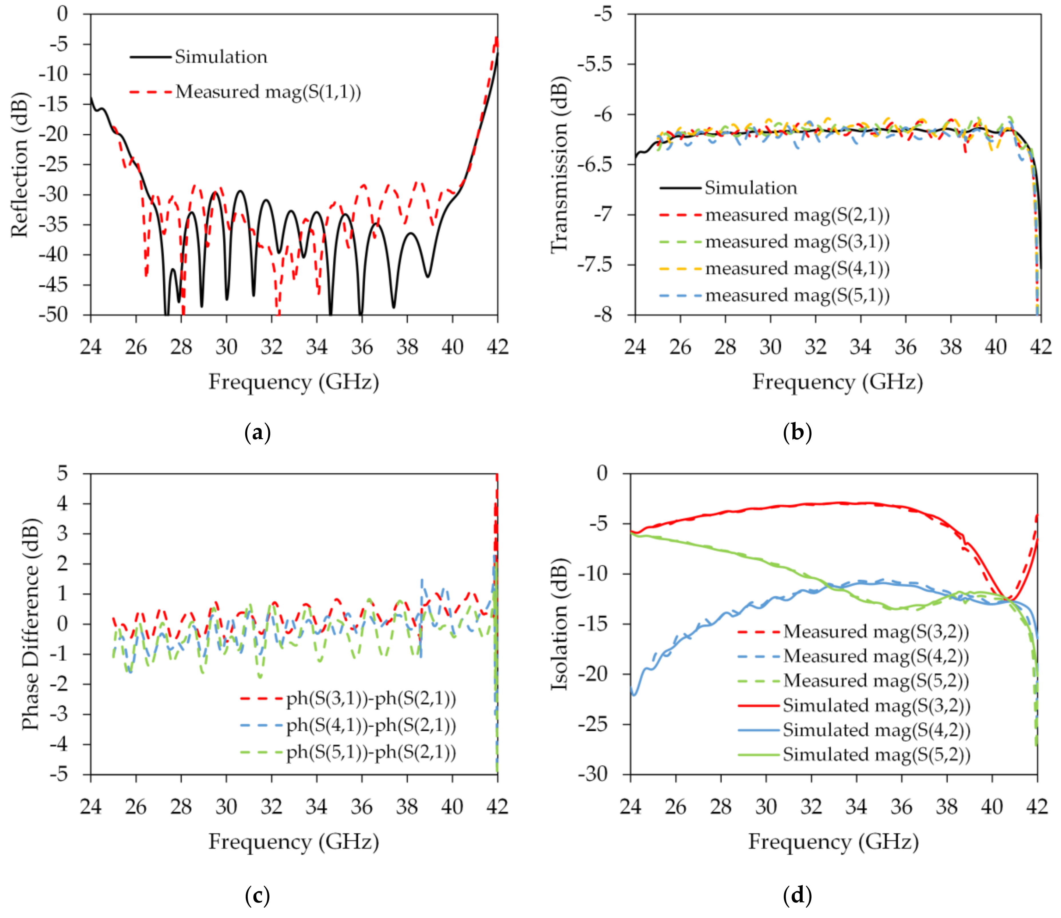
4. Power Divider/Combiner Characterization and Results

The power divider was implemented in two aluminum layers, stacked in a platelet configuration. Layer 1 only included the central scatterer and the output ports straight waveguide sections, whereas the rest of the structure was mechanized in layer 2, as shown in Figure 10. The total length of the layers was 190 mm and the width of each output arm was 20 mm. Heights were 10 mm for Layer 1 and 11.78 mm for Layer 2.
A picture of the disassembled power divider is presented in Figure 11a, while in Figure 11b a photograph of the circuit under test conditions is included.
The power divider was characterized by using the vector network analyzer (VNA) model N5227A from Keysight Technologies, connected to coaxial-to-WR28 commercial transitions, and the Ka-band calibration kit model R11644A. The thru-reflect-line (TRL) calibration technique was applied at waveguide interface, so the calibration plane was established at the power divider input/output ports, enabling its full characterization. Since the structure has five ports, the remaining ports during each measurement were loaded with precision waveguide matched terminations.
A first set of measurements were taken with VNA port 1 connected to power divider common port, and VNA port 2 connected to each power divider output port successively. From these measurements, the return loss of each port was obtained as well as the input–output insertion loss and the different phase differences, if any, between transmission signals. These results are presented in Figure 12a to Figure 12c, where the simulated curves were also included for a better comparison.
A second set of measurements were performed with VNA port 1 connected to one output port, and VNA port 2 connected to the remaining output ports successively, while the power divider common port was suitably loaded. From these measurements the isolation between output ports could be obtained. Due to the configuration of this structure, the isolation values were inherently poor. As commented in the Introduction section, these values could be improved, if needed, by adding a sixth port rotated 90° with respect to the input port in the turnstile junction [24,25]. This solution improves the isolation between ports, but narrows the usable bandwidth. However, if the power amplifiers to be connected to the output ports exhibit very low values of reverse gain, as is the case, then high values of isolation are not required for a good performance. The measured isolation values are presented in Figure 12d.
As can be seen in Figure 12a, the measured return loss at common port was around 30 dB, which was in agreement with the result predicted in the simulation. On the other hand, the measured insertion loss, plotted in Figure 12b, had a mean value of 0.18 dB in the band of interest, which agreed well with the simulated value in HFSS, taking into account the used electrical conductivity value.
In Figure 12c, taking one of the transmission measurements as a reference, the phase difference or phase error of the other transmission measurements, with respect to this reference, was calculated and plotted. These phase differences between transmission branches were kept very low, which minimized the loss of efficiency. Finally, the isolation values presented in Figure 12d met the theoretical values for this kind of structure. Table 3 presents a brief comparison between the results measured in this work and other results from turnstile-based power combiner/dividers found in the literature. From these results, the significant improvement in electrical performance was evident, in bandwidth, return loss, and power handling capability, with respect to previously published works.

5. Conclusions

This work introduces, for the first time, a true full-band (40%) waveguide four-way power divider/combiner specifically designed for high-power applications at the Ka-band. The device is based on an evolved turnstile junction with a rectangular input port rotated 45°, which equally divides the input power among the output ports. The full-band performance is obtained thanks to the inclusion of an oversized cavity together with suitably designed matching sections. The circuit is completed with E-plane bends and long waveguide arms to accommodate existing power amplifiers. Measured results show an excellent performance with around 30 dB of return loss at the common port and 0.18 dB of insertion loss, which minimizes thermal heating. Phase difference between branches is lower than 1.5°, which has minimum impact on the combiner efficiency. The designed power divider/combiner is suitable for its assembly with power amplifiers in order to obtain very high-power structures (up to several kW).

Author Contributions

Conceptualization, J.L.C., F.D.P., and A.M.; funding acquisition, P.C.; investigation, J.L.C., F.D.P., and A.M.; supervision, A.M. and P.C.; validation, J.L.C.; writing—original draft, J.L.C.; writing—review and editing, F.D.P., A.M., and P.C.

Funding

This research was developed under the National Project 2015CPC2MA, funded by the Italian Ministry of Instruction, University and Research (MIUR).

Conflicts of Interest

The authors declare no conflicts of interest. The funders had no role in the design of the study; in the collection, analyses, or interpretation of data; in the writing of the manuscript, or in the decision to publish the results.

References

  1. Moron, J.; Leblanc, R.; Lecourt, F.; Frijlink, P. 12W, 30% PAE, 40 GHz power amplifier MMIC using a commercially available GaN/Si process. In Proceedings of the 2018 IEEE/MTT-S International Microwave Symposium-IMS, Philadelphia, PA, USA, 10–15 June 2018; pp. 1457–1460. [Google Scholar]
  2. Yamaguchi, Y.; Kamioka, J.; Hangai, M.; Shinjo, S.; Yamanaka, K. A CW 20W Ka-band GaN high power MMIC amplifier with a gate pitch designed by using one-finger large signal models. In Proceedings of the 2017 IEEE Compound Semiconductor Integrated Circuit Symposium (CSICS), Miami, FL, USA, 22–25 October 2017; pp. 1–4. [Google Scholar]
  3. Gasmi, A.; Kaamouchi, M.E.; Poulain, J.; Wroblewski, B.; Lecourt, F.; Dagher, G.; Frijlink, P.; Leblanc, R. 10W power amplifier and 3W transmit/receive module with 3 dB NF in Ka band using a 100nm GaN/Si process. In Proceedings of the 2017 IEEE Compound Semiconductor Integrated Circuit Symposium (CSICS), Miami, FL, USA, 22–25 October 2017; pp. 1–4. [Google Scholar]
  4. Ng, C.Y.; Takagi, K.; Senju, T.; Matsushita, K.; Sakurai, H.; Onodera, K.; Nakanishi, S.; Kuroda, K.; Soejima, T. A 20-watt Ka-band GaN high power amplifier MMIC. In Proceedings of the 2014 44th European Microwave Conference, Rome, Italy, 6–9 October 2014; pp. 1348–1351. [Google Scholar]
  5. Yin, Z.; Shao, Z.; Liu, L.; Zhu, X. Design of a Novel Broadband Power Divider Based on Oversized-Coaxial and Radial Waveguide. In Proceedings of the 2011 International Conference on Computational Problem-Solving (ICCP), Chengdu, China, 21–23 October 2011. [Google Scholar]
  6. Ning, Y.; Sun, J.; Liu, J.; Jiang, W. A New Spatial Power Combiner Based on 32-way Ridged Waveguides. In Proceedings of the XXXIth URSI General Assembly and Scientific Symposium (URSI GASS), Beijing, China, 16–23 August 2014. [Google Scholar]
  7. Kazemi, R.; Hegazi, G.; Fathy, A.E. X-band All-Waveguide Radial Combiner for High Power Applications. In Proceedings of the 2015 IEEE MTT-S International Microwave Symposium, Phoenix, AZ, USA, 17–22 May 2015. [Google Scholar]
  8. Jia, P.; Chen, L.-Y.; Alexanian, A.; York, R.A. Multioctave Spatial Power Combining in Oversized Coaxial Waveguide. IEEE Trans. Microw. Theory Techn. 2002, 50, 1355–1360. [Google Scholar]
  9. Song, K.; Xue, Q. Planar Probe Coaxial-Waveguide Power Combiner/Divider. IEEE Trans. Microw. Theory Techn. 2009, 57, 2761–2767. [Google Scholar] [CrossRef]
  10. Abdolahi, M.; Sabahi, M.M.; Pourgholamhossein, Z.; Sadeghi, H.M. Broadband Eight-way Coaxial Waveguide High Power Combiner/Divider. In Proceedings of the 2017 Progress In Electromagnetics Research Symposium-Spring (PIERS), St. Petersburg, Russia, 22–25 May 2017. [Google Scholar]
  11. Leggieri, A.; Passi, D.; Di Paolo, F. The Squarax Amplifier: An Electromagnetic and Thermo-Mechanical Innovation. In Proceedings of the Progress In Electromagnetics Research Symposium (PIERS), Guangzhou, China, 25–28 August 2014; pp. 2273–2280. [Google Scholar]
  12. Leggieri, A.; Passi, D.; Di Paolo, F.; Orengo, G. The Squarax Spatial Power Combiner. Prog. Electromagn. Res. C 2013, 45, 43–55. [Google Scholar] [CrossRef]
  13. Coaxial Connector Average Power Handling Graph. Available online: http://mpd.southwestmicrowave.com (accessed on 22 January 2019).
  14. Cheng, N.-S.; Alexanian, A.; Case, M.G.; York, R.A. 20 Watt Spatial Power Combiner in Waveguide. In Proceedings of the 1998 IEEE MTT-S International Microwave Symposium Digest, Baltimore, MD, USA, 7–12 June 1998. [Google Scholar]
  15. Leggieri, A.; Passi, D.; Di Paolo, F.; Saggio, G. Global Design of a Waveguide X-Band Power Amplifier. Int. J. Simul. Syst. Sci. Technol. 2014, 15, 68–74. [Google Scholar]
  16. Jiang, X.; Ortiz, S.C.; Mortazawi, A. A Ka-Band Power Amplifier Based on the Traveling-Wave Power-Dividing/Combining Slotted-Waveguide Circuit. IEEE Trans. Microw. Theory Techn. 2004, 52, 633–639. [Google Scholar] [CrossRef]
  17. Kang, Z.-Y.; Chu, Q.-X.; Wu, Q.-S. A Ka-Band Broadband Traveling-Wave Power Divider/Combiner Based on Low-Loss Septum Unsymmetrical E-plane T-junction Series. In Proceedings of the 2012 IEEE/MTT-S International Microwave Symposium Digest, Montreal, QC, Canada, 17–22 June 2012. [Google Scholar]
  18. Kang, Z.; Chu, Q.; Wu, Q. A Compact Ka-Band Broadband Waveguide-Based Traveling-Wave Spatial Power Combiner with Low Loss Symmetric Coupling Structure. Prog. Electromagn. Res. Lett. 2013, 36, 181–190. [Google Scholar] [CrossRef]
  19. Garcia, J.A.; Kosmopoulos, S.; Goussetis, G. A Compact 12-way Slotted Waveguide Power Combiner for Ka-Band Applications. IEEE Microw. Wireless Comp. Lett. 2017, 27, 135–137. [Google Scholar] [CrossRef]
  20. Epp, L.W.; Hoppe, D.J.; Khan, A.R.; Stride, S.L. A High-Power Ka-Band (31-36 Ghz) Solid-State Amplifier Based on Low-Loss Corporate Waveguide Combining. IEEE Trans. Microw. Theory Techn. 2008, 56, 1899–1908. [Google Scholar] [CrossRef]
  21. Zang, F.; Song, K.; Li, G.; Zhao, M. Sub-THz Four-Way Waveguide Power Combiner with Low Insertion Loss. J. Infrared Milli. Terahz. Waves 2014, 35, 451–457. [Google Scholar] [CrossRef]
  22. Bo, S.; Bin, L.; Weng, L.S.; Wenjiang, W. Millimeterwave Eight-way Waveguide Combiner for High Power Combining. In Proceedings of the 2016 IEEE Region 10 Conference (TENCON), Singapore, 22–25 November 2016. [Google Scholar]
  23. Deng, J.; Wang, Q.; Zhao, P.; Tian, M.; Li, Q. A Quasi-Planar H-Plane Waveguide Power Divider with Full Bandwidth. IEEE Microw. Wireless Comp. Lett. 2018, 28, 645–647. [Google Scholar] [CrossRef]
  24. Eisenhart, R.L.; Nevils, N.W.; Gulick, J.J.; Monzello, R.C. A Matched Turnstile Type 4-way Divider/Combiner. In Proceedings of the 1983 IEEE MTT-S International Microwave Symposium Digest, Boston, MA, USA, 31 May–3 June 1983; pp. 166–168. [Google Scholar]
  25. Grubinger, H.; Barth, H.; Vahldieck, R.A. Low-Loss, Wideband Combiner for Power Amplification at Ka-Band Frequencies. In Proceedings of the 2008 IEEE MTT-S International Microwave Symposium Digest, Atlanta, CA, USA, 15–20 June 2008. [Google Scholar]
  26. Wang, M.; Xie, X.; Zhao, X.; Zhou, L. A Compact Four-Way Power Combiner/Divider in W-Band. In Proceedings of the 2013 Cross Strait Quad-Regional Radio Science and Wireless Technology Conference, Chengdu, China, 21–25 July 2013; pp. 47–50. [Google Scholar]
  27. Zhang, F.; Song, K.; Fan, M.; Fan, Y. All-Metal-Waveguide Power Divider with High Power-Combining Efficiency. J. Infrared Milli. Terahz. Waves 2016, 37, 258–266. [Google Scholar] [CrossRef]
  28. Passi, D.; Leggieri, A.; Di Paolo, F.; Bartocci, M.; Tafuto, A. Spatial Power Combiner Technology. In Proceedings of the Progress in Electromagnetics Research Symposium (PIERS), Prague, Czech Republic, 6–9 July 2015; pp. 932–938. [Google Scholar]
  29. Cano, J.L.; Tribak, A.; Hoyland, R.; Mediavilla, A.; Artal, E. Full Band Waveguide Turnstile Junction Orthomode Transducer with Phase Matched Outputs. Int. J. RF Microw. CAE 2010, 20, 333–341. [Google Scholar] [CrossRef]
  30. Tribak, A.; Cano, J.L.; Mediavilla, A.; Boussouis, M. Octave bandwidth compact turnstile-based orthomode transducer. IEEE Microw. Wireless Comp. Lett. 2010, 20, 539–541. [Google Scholar] [CrossRef]
  31. Navarrini, A.; Plambeck, R.L. A Turnstile Junction Waveguide Orthomode Transducer. IEEE Trans. Microw. Theory and Techn. 2006, 54, 272–277. [Google Scholar] [CrossRef]
  32. Passi, D.; Leggieri, A.; Di Paolo, F.; Bartocci, M.; Tafuto, A. Design of High Power Density Amplifiers: Application to Ka Band. J. Infrared Milli. Terahz. Waves 2017, 38, 1252–1263. [Google Scholar] [CrossRef]
  33. OMMIC Foundry Webpage. Available online: www.ommic.fr/site/company-1 (accessed on 22 January 2019).
  34. UMS Foundry Webpage. Available online: www.ums-gaas.com/tag/gan/ (accessed on 22 January 2019).
  35. QORVO Foundry Webpage. Available online: www.qorvo.com/gan (accessed on 22 January 2019).
  36. Northrop Grumman Foundry Webpage. Available online: www.northropgrumman.com/BusinessVentures/Microelectronics/Pages/GaNSharedRun.aspx (accessed on 22 January 2019).
  37. Rosker, M.J. Recent Advances in GaN-on-SiC HEMT Reliability and Microwave Performance within the DARPA WBGS-RF Program. In Proceedings of the 2007 IEEE Compound Semiconductor Integrated Circuits Symposium, Portland, OR, USA, 14–17 October 2007; pp. 1–4. [Google Scholar]
  38. Lidow, A.; Strittmatter, R.; Zhou, C.; Yanping, M. Enhancement mode gallium nitride transistor reliability. In Proceedings of the 2015 IEEE International Reliability Physics Symposium, Monterey, CA, USA, 19–23 April 2015; pp. 2–2. [Google Scholar]
  39. Zanoni, E.; Meneghesso, G.; Meneghini, M.; Stocco, A.; Dalcanale, S.; Rampazzo, F.; De Santi, C.; Rossetto, I. Reliability of Gallium Nitride microwave transistors. In Proceedings of the 2016 21st International Conference on Microwave, Radar and Wireless Communications (MIKON), Krakow, Poland, 9–11 May 2016; pp. 1–6. [Google Scholar]
  40. Zhao, X.; Xu, R.; Xu, Y. An improved nonlinear thermal resistance extraction method for AlGaN/GaN HEMTs. In Proceedings of the 2015 IEEE International Conference on Communication Problem-Solving (ICCP), Guilin, China, 16–18 October 2015; pp. 261–263. [Google Scholar]
Figure 1. 3D sketch of the turnstile-based junction in the proposed power divider.
Electronics 08 00193 g001
Figure 2. Junction design parameters definition in: (a) side view and; (b) top view.
Electronics 08 00193 g002
Figure 3. Simulated performance of the proposed junction; reflection at common port in red lines and input-output transmission in blue lines. Results from µWave Wizard in dashed lines and from HFSS in solid lines.
Electronics 08 00193 g003
Figure 4. E-plane bend with design parameters definition. Sections to be mechanized in each layer are also indicated.
Electronics 08 00193 g004
Figure 5. Simulated reflection of the designed E-plane bend. Results from µWave Wizard in dashed blue line and from HFSS in solid red line.
Electronics 08 00193 g005
Figure 6. Power divider structure as simulated in ANSYS HFSS.
Electronics 08 00193 g006
Figure 7. Simulated performance of the whole power divider structure; reflection at common port in red lines and input–output transmission in blue lines. Results from µWave Wizard in dashed lines and from HFSS in solid lines. Insertion loss from HFSS obtained with an aluminum electrical conductivity of σ = 3.8 × 10⁷ S/m.
Electronics 08 00193 g007
Figure 8. Simulation of the electric field within the junction. The maximum value is obtained at the sharp edges of the central scatterer.
Electronics 08 00193 g008
Figure 9. A representation of the complete HPA, using two combiners and four SPAs. Size is 290 × 290 × 140 mm.
Electronics 08 00193 g009
Figure 10. 3D sketch of the designed power divider implemented in layers: (a) view from top; (b) view from bottom.
Electronics 08 00193 g010
Figure 11. Photographs of the power divider: (a) disassembled; (b) under test.
Electronics 08 00193 g011
Figure 12. Measured results of the proposed power divider/combiner: (a) reflection at common port (simulation with HFSS in solid red line and measurement in dashed blue line); (b) transmission from input port to all output ports (simulation with HFSS in solid black line and measurements in dashed colored lines); (c) measured phase differences between transmission measurements and a transmission measurement taken as a reference; (d) isolations between output ports (simulations with HFSS in solid lines and measurements in dashed lines). Opposite ports in red lines and orthogonal ports in blue and green lines.
Electronics 08 00193 g012
Table 1. Junction design parameters values.
ParameterValue (mm)ParameterValue (mm)
a7.1l06.64
b3.56acav7.26
arec6.35lcav1.23
brec3.84d14.67
lrec1.25h10.56
dcir8.92d22.50
lcir0.33h21.22
Table 2. E-plane bend design parameters values.
ParameterValue (mm)ParameterValue (mm)
s10.47h22.22
s22h30.76
s32.69l110
h12.87Rtool0.6
Table 3. Performance comparison between turnstile-based power combiner/dividers.
ReferenceBandwidth (GHz)Return Loss (dB)Insertion Loss (dB)Power Capability (kW)
[25]~31–38 (20%)20~0.1-
[26]85–100 (16%)22
(simulated)
0.04
(simulated)
-
[27]82–107 (26%)14.50.56.8 (theoretically)
This work26.5–40 (40%)300.1810.3 (theoretically)

