A Simple Closed-Loop Active Gate Voltage Driver for Controlling diC/dt and dvCE/dt in IGBTs


Department Electronic, MCIA research center, Universitat Politècnica de Catalunya (UPC), 08222 Terrassa, Spain
*
Author to whom correspondence should be addressed.
Electronics 2019, 8(2), 144; https://doi.org/10.3390/electronics8020144
Submission received: 23 December 2018
/
Revised: 20 January 2019
/
Accepted: 28 January 2019
/
Published: 30 January 2019
(This article belongs to the Section Microelectronics)
Abstract
:The increase of the switching speed in power semiconductors leads to converters with better efficiency and high power density. On the other hand, fast switching generates some consequences like overshoots and higher switching transient, which provoke electromagnetic interference (EMI). This paper proposes a new closed-loop gate driver to improve switching trajectory in insulated gate bipolar transistors (IGBTs) at the hard switching condition. The proposed closed-loop gate driver is based on an active gate voltage control method, which deals with emitter voltage (VEe) for controlling diC/dt and gets feedback from the output voltage (vCE) in order to control dvCE/dt. The sampled voltage signals modify the profile of the applied gate voltage (vgg). As a result, the desired gate driver (GD) improves the switching transients with minimum switching loss. The operation principle and implementation of the controller in the GD are thoroughly described. It can be observed that the new GD controls both dvCE/dt and diC/dt accurately independent of the variable parameters. The new control method is verified by experimental results. As a current issue, the known trade-off between switching losses and EMI is improved by this simple and effective control method.
1. Introduction
Insulated gate bipolar transistor (IGBT) power semiconductors with antiparallel freewheeling diodes (FWDs) are widely employed in industrial applications. In order to achieve high-density power converters, attention is focused on the use of fast IGBTs. Hence, the demand for minimizing switching losses and increasing efficiency has encouraged engineers to design more effective IGBT gate drivers. For gate drive (GD) designing, the main task is transient behavior improvement in switching times with minimum penalty in the losses. It is well known that fast switching has a direct effect on the minimization of switching losses; meanwhile, it is the major reason for electromagnetic interference (EMI) generation in switched-mode power converters [1]. Moreover, the higher rates of voltage and current transition (dvCE/dt and diC/dt respectively) impose stress on the IGBT, which has a harmful effect on device lifetime [2]. Therefore, a trade-off between switching losses and EMI generation should be defined for optimized switching. This will be more challenging when we are dealing with IGBTs, which operate at high frequency and are under hard switching conditions over non-constant load.
In addition, the other challenging issue in GD designing is the definition of diC/dt and dvCE/dt rates and keeping them in the desired values during operation condition, independent of effective variables such as junction temperature (Tj), parasitic inductance (LS), and load etc. [3]. Moreover, some other factors such as high-speed operation, low-cost production, simplicity in structure, effectiveness in EMI reduction, and efficiency improvement are important considerations in GD designing. The modification of gate resistor (Rg) in the drive circuit is known as a conventional solution for the switching control [4,5,6]. The result of using a conventional gate drive (CGD) is a sub-optimal compromise, which has an undesirable effect on the switching speed and switching losses of IGBTs. To overcome the inherent ineffectiveness of CGDs, many active gate controls (AGC) have been reported [3,7,8,9,10,11,12,13,14,15,16,17,18,19,20,21,22,23,24]. In order to create a safe operating point for an IGBT with respect to its nonlinearities and dependencies, it is necessary to get some feedback to related concerns and apply them to the GD controller. For this reason, using passive and feedforward controllers with a simple structure and cheaper price is not an ideal solution for industrial applications. Therefore, AGC can mainly be categorized into the closed-loop controller’s family. These controllers have been presented and gradually developed to guarantee the safe operation area (SOA) of IGBTs under different load conditions. However, using such controllers increases the cost and complexity of the GDs circuit. For this reason, the goal is to achieve a cost-effective and simple closed-loop controller with respect to robustness factors.
The junction temperature and the load variation as changeable factors and IGBTs’ nonlinearity have a significant influence on the structure of closed-loop GDs. A brief review of these factors is summarized here. As an exclusive advantage of this controller, the proposed GD operates no dependence on the mentioned factors.
1.1. Junction Temperature (Tj)
The reliability of IGBTs is a thermal-related issue; as much as half of the total amount of power-related device damage is related to temperature-dependent failures [25,26]. However, the effect of high Tj is not limited to reliability. This factor has a significant effect on IGBT switching characteristic values [27], as it may change the dynamic behaviour of gate voltage (VGe) and current (iG). Furthermore, threshold gate-emitter voltage (VGe,th) may vary with different temperatures [28,29,30]. Therefore, considering Tj for some of the controllers that are dealing with gate side parameters is essential. Otherwise, the applied controller may not be entirely effective for all operating conditions. For instance, an active gate voltage control was presented in [11] to control the values of diC/dt and dvCE/dt at turn on/off, based on gate side transient behaviour. However, the addressed intervals may vary by different Tj values, which are the principal action of the controller. The defined intervals for controller operation have been restricted by constant delays, hence, for such controllers, some criticisms can be raised. Different methods for measuring device temperature have been presented [31]. The proposed closed-loop GD presented in this paper is independent of the temperature of the IGBT. It covers all consequences of temperature variation without installing an additional circuit.
1.2. Load Variation
Missing compensation of the load variation is the main drawback of passive and feedforward controllers [3]. Thereby, the closed-loop concept with negative feedback is promoted to achieve more precise control. The variation in the load affects dvCE/dt and diC/dt. Especially in hard switching condition when IGBT operates under inductive loads, preserving the dvCE/dt and diC/dt in proportional slope rates is a serious issue for EMI standards [32]. Moreover, the load and its demanded current have an effect on the Miller plateau area in the IGBT during turn on/off transients [33]. This factor, as in the previous section, may change the behavior of the IGBT in the gate side, and all previous concerns are valid for this case as well. Significantly, in turn-on condition, the load variation affects diC/dt so that it also has an effect on the inducted “vEe” voltage that exists between the emitter and the common path of the converter. This voltage, which has been created by stray inductance, is used in the proposed controller. Using this technique, the GD has been benefited by an undesirable phenomenon. More details are explained in the corresponding section. Briefly, the IGBT can be controlled permanently in all load conditions.
1.3. IGBT’s Nonlinearity
Typically, the closed-loop AGC is the only possible solution to compensate for the IGBT’s nonlinearities in variable operating conditions. Many sophisticated analog closed-loop GDs have been presented [9,17,34,35,36]. Due to the different transient behavior of IGBTs at each switching on/off condition [37,38,39], individual control loops for each switching state (for diC/dt control at turn-on [18], or dvCE/dt at turn-off [40]) are needed. In addition, for full GDs a combination of both voltage and current feedback in the AGC topology have been presented [3,8,24]. Recently, several digital approaches have been presented in IGBT GDs [19,20,21], [33,41]. The use of these techniques has benefits for minimization of switching losses, reverse-recovery current, and EMI at desired switching operation. However, the large delay times during conversion of analog to digital (A/D), and vice versa (D/A), in the signal paths and the higher cost are the main drawbacks of digital solutions. In contrast, this paper proposes a simple analog GD that controls both voltage and current transitions in a closed loop.
Various methods for diC/dt controlling based on the measurement of the collector current have been presented herein, and many different techniques for controlling dvCE/dt through the measurement of the collector-emitter voltage have also been proposed. However, the proposed GDs have been mainly complicated and expensive solutions or, in other cases, they sacrifice additional switching losses. In this study, a simple structure closed-loop GD with voltage type feedback operates independently of variable parameters while maintaining a precise balance between switching losses and EMI effects. The concept, principles, and structure of the proposed control method are explained in Section 2. The controller setting and performance of the new closed-loop GD is evaluated using experimental results, which are presented in Section 3. Section 4 presents a performance index of the new GD through comparisons with conventional gate drive methods. EMI analysis and cost are also evaluated here. The paper closes with a discussion of the presented controller and conclusion.
2. Proposed Active Gate Control Method
The proposed GD controls the IGBT’s diC/dt and dvCE/dt at turn-on and turn-off, respectively. The rise in collector current during turn-on switching creates a vEe voltage at the IGBT emitter, which is used in the controller as feedback. The output voltage (VCE) as turn-off feedback is applied to the closed-loop controller as well. The principles of the new GD are based on the active gate voltage control method. Thus, an intermediate gate-voltage (vgg) is applied at specific intervals, which covers current (iC) rise time at turn-on and voltage (VCE) rise time at turn-off. The level of the applied intermediate voltage varies due to the load variation in order to maintain the desired rates for current and voltage transitions. The concept and operation principle of the new closed-loop GD is explained below.
2.1. Philosophy of the Method
The IGBT meets several intervals during its turn on/off under hard switching conditions. Figure 1 shows these intervals schematically. All the details regarding the switching process of the IGBT are fairly well documented in [39]. Here, we have mainly focused on the corresponding intervals to figure out the effective parameters and control the diC/dt and dvCE/dt rates.
At t0, a voltage step (from −VEE to +VCC) is applied to the gate port. At this moment, the gate current (iG) immediately rises to its maximum value and then starts to decay. In the meantime, the gate voltage vGe rises in accordance with the time constant (τG) of the charging process cf. Equations (1) and (2). The IGBT is still off as long as the vGe remains lower than the threshold voltage vGe;th. This process happens in the first interval, which covers the time between t0 to t1 cf. Figure 1a. This interval is a so-called gate charge delay and it has a minimal effect on diC/dt rate; however, the gate charge has remained valid and the potential energy is stored for the next interval.
As soon as vGe(t) passes the vGe,th value, the GD circuit changes the profile of the vgg voltage signal and delivers a lower voltage value to the gate-emitter (see Figure 1a). In this moment, the IGBT begins to conduct current based on its transfer and output characteristics. Then, the collector current increases almost linearly from zero, and the load current initiates commutation from the freewheeling diode to the IGBT [39]. The extra gate charge that had been stored in the previous interval can potentially generate the overshoot problem in iC [42,43]. According to equations below, which have been proved in [17,23], the diC/dt rates can be calculated as a function of the gate circuit parameter. The gate current iG (t) during the second interval can be represented as
That ∆vgg is the difference value of the maximum (VCC) and minimum (VEE) gate drive voltage, and Rg is the gate resistor.
The iC and diC/dt equations in turn-on can be approximately explained as
where gm is the IGBT’s linearized transconductance.
CGC is Miller capacitance; IF is the diode forward current; BVBD is the diode breakdown voltage and LS is the stray inductance.
The collector current iC rises rapidly when vGe(t) exceeds vGe,th value, cf. Equation (5). Whereas, in high voltage applications (in high vCE values), CGe is too small; therefore, according to Equation (7), the only possible way to obtain the desired diC/dt rate is to have constant product in gm·iG. Hence, the transconductance gm or gate current value during the current rise time should be controlled. Furthermore, the overshoot in collector current IOS may appear because of the reverse recovery current that is cycling by the freewheeling diode (FWD), cf. Equation (8).
The gate-emitter capacitance depends on the physical structure of the IGBT, so diC/dt control at turn-on condition can be possible by changing the vGe or gate current iG values. In Figure 1a, the gray background demonstrates the controller operation time to apply the intermediate vgg voltage value. Based on this technique, the injected iG will be controlled by changing the vgg voltage profile, cf. Equation (3), in order to control diC/dt, cf. Equation (7), and remove the current overshoot, cf. Equation (8).
Figure 1b shows schematic waveforms of the IGBT at turn-off. At t6, the vgg voltage pulse is switched to its negative value. With a few exceptions, it can be assumed that voltage and current in the gate side have inverse behavior compared to turn-on condition. Upon applying VEE, the vGe(t) starts to decay, and at the same time, vCE gradually increases. The slow rising in vCE is because of the large Miller capacitance CGC value. In this process, as soon as both vCE and vGe arrive at the same value, CGC suddenly falls down in value and the vCE starts to rise fast [39]. The dvCE/dt can be calculated as
This transition also directly depends on the gate current. Therefore, the method of active gate voltage control could be an effective solution. As shown in Figure 1b, at t8, as soon as VCE exceeds the vGe value, VCE starts its fast rising until t9. This uptrend is continued as loge as the vCE gets the value of VDC. During this period, the new controller applies a lower voltage to the gate circuit, according to the load condition.
2.2. The Operation Principles
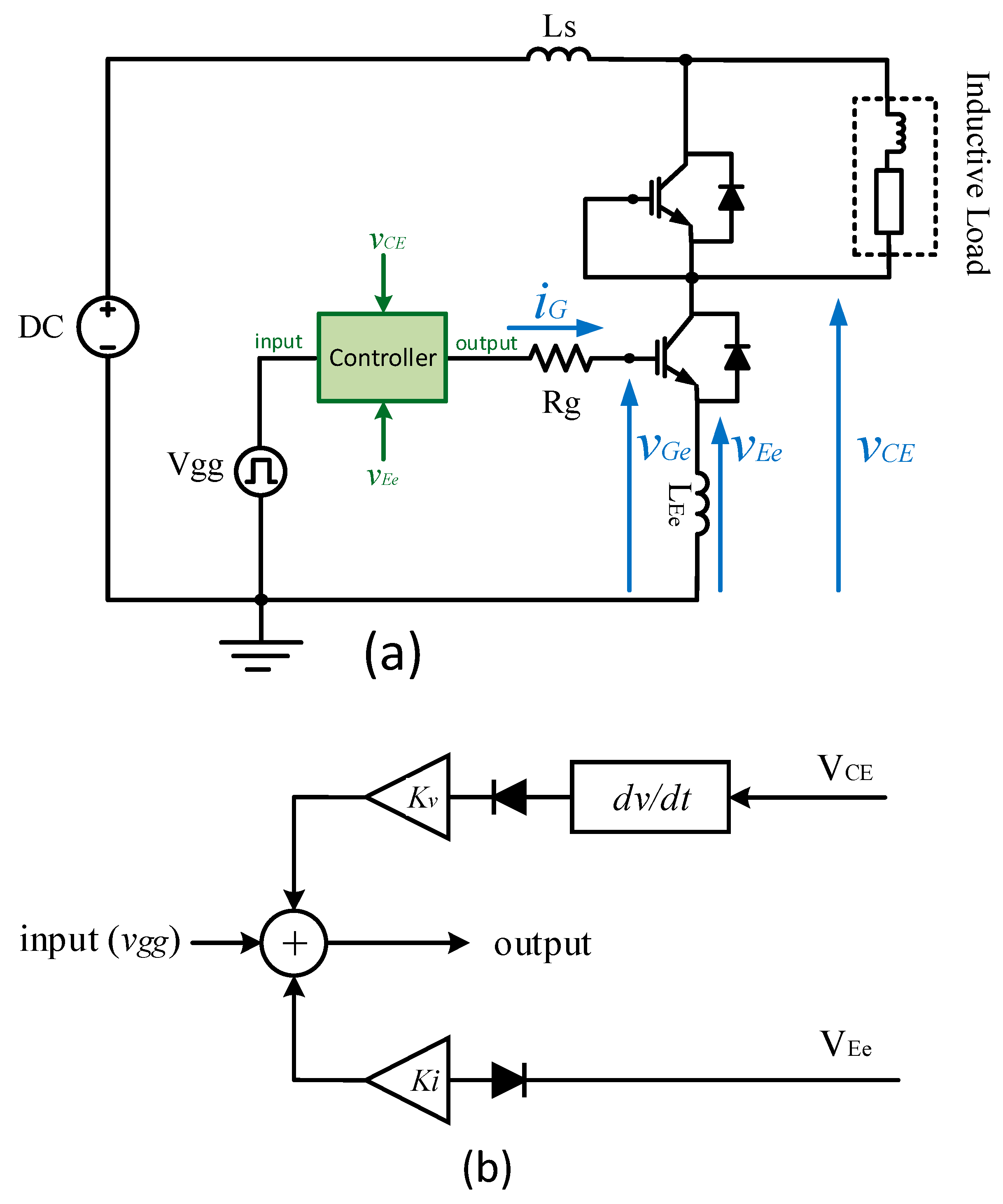
The schematic of the case study and the topology of the new GD are presented in Figure 2. More details regarding the load and circuit component are reflected in Appendix A.
In real condition, an inductance exists between emitter and earth. This inductive factor (LEe) is a part of stray inductance (LS), and its value mainly depends on the designed printed circuit board (PCB) layout [44]. During turn-on condition, diC/dt gets a value and LEe generates a voltage (vEe), cf. Equation (10). Based on Lenz’s law, the induced voltage has inverse polarity. The positive part of vEe, which had been created by the current decaying (see Figure 3), is filtered by a diode (see Figure 2b). The created vEe voltage has diC/dt factor in itself inherently and that can be used as feedback in the active gate voltage controller instead of getting feedback from the output current. This technique has obvious advantages. For instance, it is simpler because the use of a current sensor would make the circuit more complicated. In conventional closed-loop diC/dt controllers [3,17], in order to sense error, the measured iC must be derived in feedback. However, in addition to the use of extra operation (typically by Op-Amp), the transfer function gets an extra dimension, which increases the sensibility of the controller from the stability aspect. Therefore, it can be said that the proposed active gate voltage control method with a simpler structure is more robust as well.
To achieve the desired diC/dt and proper transient, the obtained vEe voltage is adjusted by a Ki coefficient and it is used to reduce the original vgg voltage signal. Thereby, in turn-on condition, the GD feeds the IGBT with proper intermediate voltage. Thus, a controlled current driven by this intermediate voltage at the specific interval (between t1 to t2) will be injected into the gate port.
Moreover, the proposed closed-loop GD makes it possible to control dvCE/dt at the turn-off switching. To maintain voltage transition under control, the positive part of dvCE/dt with a proportional coefficient (Kv) is summed with vgg. The configuration of the proposed closed-loop gate driver as a block diagram is shown in Figure 2b. The voltage type feedback, after summing vgg, modifies its profile. Thereby, diC/dt and dvCE/dt, during corresponding switching conditions, are controlled by this method of active gate voltage driving.
3. The Closed-Loop GD Tuning and Experimental Results
The experimental tests were performed in almost nominal voltage, and a high inductive load created hard switching conditions for the IGBT. The voltage of the dc-bus is 550 V, and the IGBT operates at 5KVA. Two DC power supplies (XFR 300V-9A, Xantrex Technology Inc., Burnaby, Canada) as a series connection provide the power for the test bench.
For each switching state, only one adjustment parameter is necessary, which should be located in the corresponding feedback paths. Through a proper Ki coefficient, a suitable voltage value will be applied to the gate. Therefore, in order to control the diC/dt at turn-on, the determination of Ki coefficient is necessary, from which a reduction on gate voltage is provoked. As a desirable purpose, a significant reduction in current overshoot and EMI problem will result.
The mathematics logic for diC/dt and dvCE/dt controlling and overshoot suppression by modification of ∆vgg is based on Section 2.1. However, the practical tuning based on the experimental behavior of the IGBT is explained here.
At turn-on condition, in order to allow the IGBT to remain in on-state, the minimum value of intermediate vgg should be higher than the threshold value (vGe,th), whose maximum value is 6.5 V for this device. Therefore, the minimum intermediate voltage (by Ki1) selected is not lower than 6.8 V. Although the IGBT stayed in the active region while applying intermediate voltage, only switching-off condition (see [39]) is able to challenge its operation; however, due to the stability and SOA considerations, the minimum Ki coefficient was selected with high margin. The reflected experimental results in Figure 4 and Table 1 show how diC/dt and the overshoot in collector current are both influenced by Ki. The desired Ki can be realized with a simple voltage divider.
The control of dvCE/dt and overshoot suppression at the turn-off switching can be achieved by the feasible solution shown in Figure 2b. The voltage transition will be under control when the controller operates with a proper Kv coefficient. Figure 5 and Table 2 present the role of choosing Kv at turn-off on the IGBT switching. It should be noted that there is a minimum limit for the differential voltage value (), which has been defined by the application note. Based on this rule, in order to apply minimum to the IGBT (during turn-off condition) and considering a safe margin, Kv1 is set on 3.5 V, which presents the slowest possible turn-off switching.
The proposed gate driver deals with the changing voltage value of the gate signal (vgg) during switching time. As we know, the IGBT in active region loses its function if the vGe (t) value is less than its threshold value. This concern has been considered by defining a safe margin area in turn-on and turn-off conditions. All the generated intermediate voltages using the GD in both switching conditions do not affect the operation of the IGBT regarding stability. It should be noted that the previous studies [11] and [45] approve the SOA of the active gate voltage driver technique on the IGBT when it operates with an intermediate voltage of vgg. However, the mentioned references were limited to manual adjusting and the feedforward control method, which are not adaptive with variable load conditions. For this reason, in this study the stability analysis was ignored.
This part does not present an optimization method for the tuning of the controller, because the new GD has a better performance index compared to CGDs in any gain value. In fact, the Tables express the trajectory of the controlling process that affects the slope current/voltage and overshoot, which consequently has an effect on efficiency and EMI. Based on this information, the user may select the level of control on the turn-on or turn-off switching. This advantage of active gate voltage control compared to conventional methods has been already approved in [11] and [45]. The new section details the performance index of the closed-loop GD.
With relation to the effect of temperature, in the Introduction we declared that the proposed closed-loop GD is independent of the IGBT’s temperature. It covers all consequences of temperature variation without installing an additional circuit. The consequence of gate side changes (e.g., temperature) can be seen on switching behaviour. This is the essence of the story and the controller may adapt itself through getting feedback from di/dt and dv/dt and applying it on the profile of the gate voltage.
Temperature influences on the switching time or/and it varies the threshold gate-emitter voltage (vGe,th) value. In the case of switching time, the controller is adaptive and it operates throughout the required switching time. However, the change in threshold voltage value is important from a SOA viewpoint and should be considered in the adjustment of the margin value of the intermediate voltages.
Several studies evaluate the variations of the threshold voltages in IGBTs [28,29]. In [29], the effect of temperature on the threshold vGe value was evaluated using different device manufacturers. The results showed that the threshold voltage in different IGBTs was reduced up to 1 V by increasing the temperature from 25 °C to 120 °C. It is a key point that the increase of temperature has a negative effect on the vGe(th) value. In fact, this change even enhances the level of the SOA when the controller reduces the gate voltage value in its operation time (see Figure 3).
4. The Performance Index of Closed-Loop GD
4.1. The Comparison with CGD
In order to evaluate the performance of the proposed GD, the obtained results using the new GD and CGD are compared together experimentally. The meaning of the CGD is the increase of gate resistor Rg value to achieve the desired transient behavior, which is a known technique [3,10,11,20,24]. In this evaluation, both control methods are compared when they have the same rate of overshoot suppression (i.e., a very similar electrical behavior, as shown in Figure 6 and Figure 7). This suppression is for current overshoot at turn-on and also for voltage overshoot at turn-off. To better understand this phenomenon, the resultant diC/dt and dvCE/dt from the new GD and CGD are compared, including the switching losses (Eon and Eoff). Figure 6 shows the current waveforms at turn-on which resulted from the new GD and CGD. At the same time, the waveforms of collector-emitter voltage are shown in Figure 7. In addition, Table 3 presents all aspects of this comparison.
The Ki1 coefficient regulates the suppression rate of the collector current. The gate resistance is increased up to 23 ohms. It should be noted that the amplitude of Rg in the original GD and in the new GD was 12 ohms, which has been calculated using the IGBT’s application note.
To realize the turn-on switching loss (Eon), vCE (t), and iC (t) waveforms should be multiplied together during the active region of the IGBT. The area of the product can be calculated using the equation below.
Where the elapsed time during t0 < t < t5 cf. Figure 1a is the turn-on switching time, then Eon is the turn-on lost energy (in joule) at each switching time.
For comparison at turn-off, the closed-loop GD operates with Kv1 coefficient, while the CGD has increased the gate resistance up to 50 ohms in order to achieve the same damping rate on voltage overshoot. The performance of both gate drivers is presented as comparative figures, which illustrate collector-emitter voltage and collector current waveforms at turn-off.
The switching loss at turn-off (Eoff) can be obtained using Equation (11) as well, but the considered domain in the calculation is t6 < t < t11, which includes turn-off switching time cf. Figure 1b. Figure 8 and Figure 9 offer a graphic comparison, and the numerical results are presented in Table 3.
It is distinguishable that the new closed-loop gate driver has improved the trade-off between switching losses and overshoot suppression.
4.2. Electromagnetic Interference Analysis
The proposed closed-loop GD has the capability of improving the dynamical behaviour of the IGBT. The high rate of current and voltage transitions (diC/dt and dvCE/dt respectively) are known reasons of EMI generation in power converters. In addition to the ability of the new GD to reduce the overshoots in output current and voltage with minimum losses penalty, it moderates the oscillation and other effective parameters, which have an impact on EMI appearance.
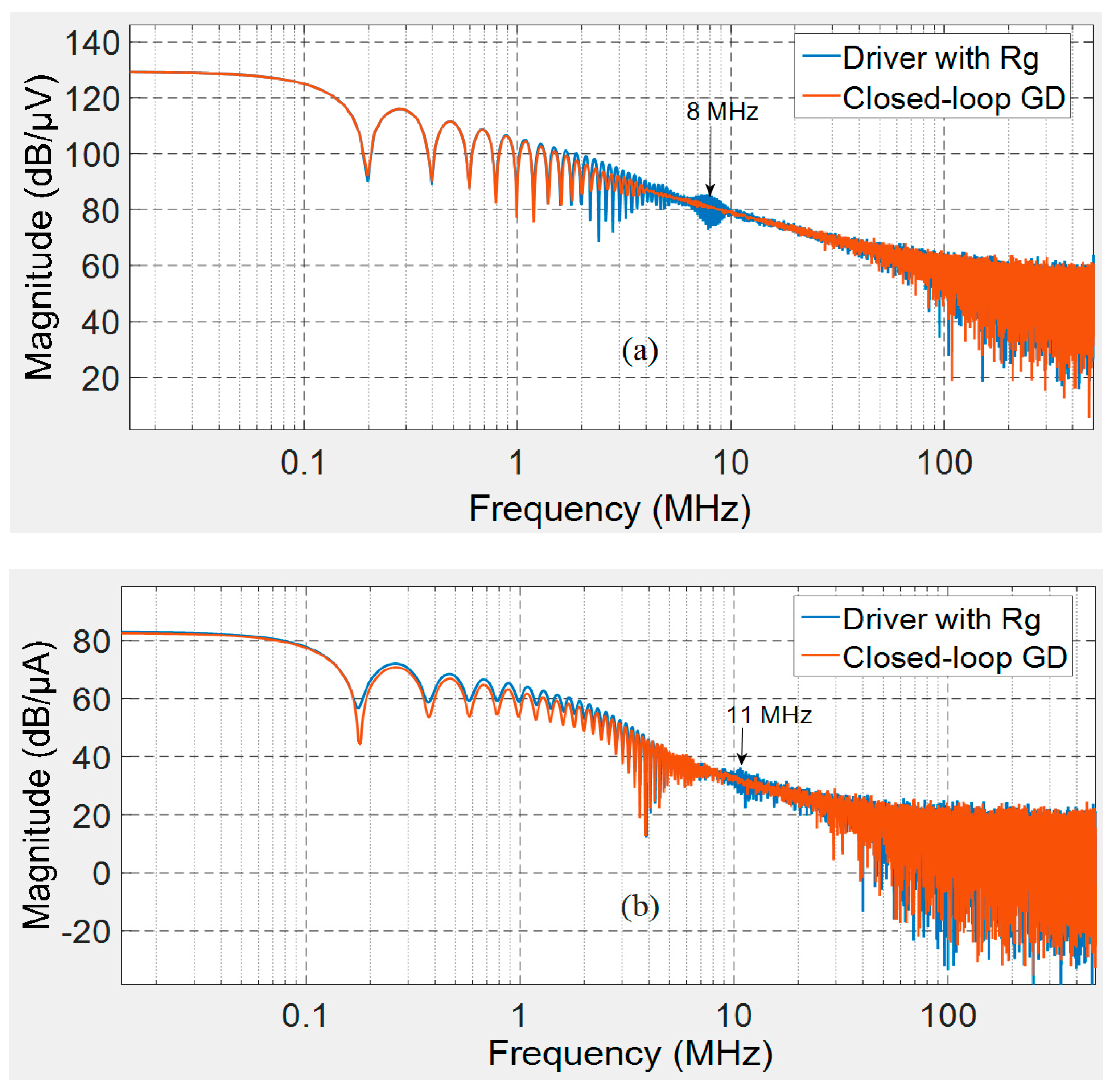
The following evaluation does not include all the aspects of EMI phenomena; however, the deference rate of EMI through driving with Rg and the new GD can be monitored. The analysis carried out is based on the trajectory of the current and voltage waveforms, which had been experimentally extracted using an oscilloscope Tektronix MDO3024 (Johnston, OH, USA). The obtained data are applied to the Fast Fourier Transform (FFT) in MATLAB software (version 2015b, MathWorks, Natick, MA, USA) for processing. The effective parameters in EMI production can be characterized using FFT analysis as a periodic trapezoidal pulse. It should be considered that the measured output current and voltage are in common mode (CM) conditions. Figure 10 shows the spectrum for both collector current and collector-emitter voltage. The results show that the closed-loop GD can eliminate the noise in VCE voltage with a resonant frequency of 8 MHz and in IC current with a resonant frequency of 11 MHz.
4.3. The Cost Study
All MOS-channel switches require a driver to supply the device and provide the desired performance. In power converters with a simple gate driver, snubber circuits are a well-known solution to reduce EMI problems and overshoots. On the other hand, snubber circuits may reduce the system efficiency and it is a large circuit for high-density power converters. However, the main advantage of snubber circuits are the cost and its simple structure. Although snubber-less methods (GD based techniques) compensate for the weak points of the snubber circuits, they increase the cost [44].
The simple structure of the proposed closed-loop GD has already been presented. In this part, the cost study is evaluated. As a reference price, the total cost of the driver plus snubber circuit is considered 1 per unit (pu), which is calculated based on the components price. Accordingly, the price of an implemented totem-pole interface unit cf. Figure A2 consisting of a pair of bipolar NPN and PNP transistors and corresponding resistors is 0.13 per unit. A pair of dual high-speed operational amplifiers and a quad general-purpose Op-Amp is 1 pu. The rest of the components, including diodes, two potentiometers, and some other resistors, represents 0.12 pu of the base cost. The cost of closed-loop GDs may be increased mainly by the high-speed comparators and MOSFETs, whereas in the proposed GD, the use of these components is not needed. As a result, in addition to its effective performance, the new closed-loop GD does not impose a significant extra cost.
In Table 4, the approximated costs of the main characteristics of the proposed closed-loop are compared to the corresponding parameters of a CGD plus snubber network.
5. Conclusions
This paper proposed a robust closed-loop gate driver for IGBTs. It has been shown that the new GD is able to improve switching transient under hard switching condition with a minimum penalization in switching loss. The following results were obtained from the experimental evaluations:
- The proposed GD has the capability to control diC/dt and dvCE/dt in turn-on and turn-off respectively. Controlling the GD is possible with very simple tuning in both switching states.
- The closed-loop GD has eliminated the overshoot from collector current by more than 20%. Furthermore, the VCE overshoot has been reduced by more than 10%. Therefore, the IGBT lifetime will be extended.
- The performance index showed that the closed-loop GD has lower switching losses compared to CGD in both turn-on and turn-off conditions.
- This novel closed-loop controller keeps its performance versus Tj and load variations without applying an extra circuit in its topology.
- Based on spectrum analysis of the current and voltage transition obtained from experimental tests, the radiated emission of EMI is reduced during switching transient.
- The proposed gate driver is simple enough to allow its use in real industrial applications. In addition, based on the evaluation carried out it is a fairly cost-effective solution.
According to the philosophy of the proposed closed-loop GD, IGBTs can be controlled permanently in all variable conditions, allowing a novel and real solution for industrial applications.
Author Contributions
Investigation, H.G., V.S., A.P.C. and J.L.R.M.; Project administration, J.L.R.M.
Funding
This research was funded by Consejo Interinstitucional de Ciencia y Tecnología, Spain CICYT TRA2013-46757-R.
Conflicts of Interest
The authors declare no conflict of interest.
Appendix A
The test circuit cf. Figure 2a, consists of the features and components below. The tested IGBT is NGTG50N60FLWG (ON Semiconductor, Phoenix, AZ, USA), clamped to 550 V DC bus-voltage. The applied inductive load is composed of RLoad = 59 Ω, L = 780 µH. The switching frequency is 20 kHz.
Figure A1 illustrates the schematic of the controller. In this circuit, the operations and integrations are done by general-purpose LT1364/LT1365 Op-amps (Linear Technology Corporation, Milpitas, CA, USA). Furthermore, both Ki and Kv coefficients are created by simple voltage divider circuits. The model of implemented diodes is 1N4148-TR.
Figure A1.
The schematic of the proposed closed-loop controller.

In order to make the connection between the closed-loop controller and IGBT, an interface unit (see Figure A2) is considered which is composed of low power bipolar NPN (2N2222) and PNP (2N2907) transistors. It was supplied by V = .
Figure A2.
Totem-pole interface unit to gate current supply.

Signal generator (Agilent 33220A-20MHz, Santa Rosa, CA, USA) generates a symmetric gate signal (). In the conventional GD method, this signal is applied to a HCPL-3120 optocoupler (Avago Technologies, San Jose, CA, USA) to have a gate signal. Since the proposed controller modifies the profile of the gate signal (vgg) and optocouplers are not able to maintain this modification, a Totem-pole interface unit (see Figure A2) generates gate signal for our driving method. The designed interface unit is able to conduct both positive and negative parts of input signals. The Totem-pole circuit does not eliminate the changes of vgg signal.
The active gate driver circuit was designed and implemented as shown in Figure A3.
Figure A3.
AGD prototype manufactured.

References
- Paul, C.R. Introduction to Electromagnetic Compatibility, 2nd ed.; Wiley: Hoboken, NJ, USA, 2006. [Google Scholar]
- Biela, J.; Schweizer, M.; Waffler, S.; Kolar, J.W. SiC versus Si—Evaluation of potentials for performance improvement of inverter and DC-DC converter systems by SiC power semiconductors. IEEE Trans. Ind. Electron. 2011, 58, 2872–2882. [Google Scholar] [CrossRef]
- Lobsiger, Y.; Kolar, J.W. Closed-Loop di/dt and dv/dt IGBT Gate Driver. IEEE Trans. Power Electron. 2015, 30, 3402–3417. [Google Scholar] [CrossRef]
- Hefner, A.R. An improved understanding for the transient operation of the power insulated gate bipolar transistor (IGBT). IEEE Trans. Power Electron. 1990, 5, 459–468. [Google Scholar] [CrossRef]
- Hefner, A.R. An investigation of the drive circuit requirements for the power insulated gate bipolar transistor (IGBT). IEEE Trans. Power Electron. 1991, 6, 208–219. [Google Scholar] [CrossRef]
- Chokhawala, R.; Catt, J.; Pelly, B. Gate drive considerations for IGBT modules. Proc. Rec. IEEE Ind. Appl. Soc. Annu. Meet. 1992, 1, 1186–1195. [Google Scholar]
- John, V.; Suh, B.S.; Lipo, T.A. High performance active drive for high power IGBTs. IEEE Trans. Ind. Electron. 1999, 35, 1108–1117. [Google Scholar]
- Park, S.; Jahns, T. Flexible dv/dt and di/dt control method for insulated gate power switches. IEEE Trans. Ind. Appl. 2003, 39, 657–664. [Google Scholar] [CrossRef] [Green Version]
- Palmer, P.; Rajamani, H. Active Voltage control of IGBTs for high power applications. IEEE Trans. Power Electron. 2004, 19, 894–901. [Google Scholar] [CrossRef] [Green Version]
- Dulau, L.; Pontarollo, S.; Boimond, A.; Garnier, J.F.; Giraudo, N.; Terrasse, O. A New Gate Driver Integrated Circuit for IGBT Devices with Advanced Protections. IEEE Trans. Power Electron. 2006, 21, 38–44. [Google Scholar] [CrossRef]
- Idir, N.; Bausiere, R.; Franchaud, J.J. Active gate voltage control of turn-on di/dt and turn-on dv/dt in insulated gate transistors. IEEE Trans. Power Electron. 2006, 21, 849–855. [Google Scholar] [CrossRef]
- Bryant, A.; Wang, Y.; Finney, S.; Lim, T.; Palmer, P. Numerical optimization of an active voltage controller for high-power IGBT converters. IEEE Trans. Power Electron. 2007, 22, 374–383. [Google Scholar] [CrossRef]
- Grbovic, P. An IGBT gate driver for feed-forward control of turn-on losses and reverse recovery current. IEEE Trans. Power Electron. 2008, 23, 643–652. [Google Scholar] [CrossRef]
- Wang, Y.; Palmer, P.; Bryant, A.; Finney, S.; Abu-Khaizaran, M.; Li, G. An analysis of high-power IGBT switching under cascade active voltage control. IEEE Trans. Ind. Appl. 2009, 45, 861–870. [Google Scholar] [CrossRef]
- Grbovi, P.; Gruson, F.; Idir, N.; le Moigne, P. Turn-on performance of reverse blocking IGBT (RB IGBT) and optimization using advanced gate driver. IEEE Trans. Power Electron. 2010, 25, 970–980. [Google Scholar] [CrossRef]
- Chen, L.; Ge, B.; Peng, F.Z. Modeling and analysis of closed-loop gate drive. In Proceedings of the Applied Power Electronics Conference and Exposition, Palm Springs, CA, USA, 21–25 February 2010; pp. 1124–1130. [Google Scholar]
- Lobsiger, Y.; Kolar, J.W. Closed-loop IGBT gate drive featuring highly dynamic di/dt and dv/dt control. In Proceedings of the IEEE Energy Conversion Congress and Exposition (ECCE), Raleigh, NC, USA, 15–20 September 2012; pp. 4754–4761. [Google Scholar]
- Fink, K.; Bernet, S. Advanced gate drive unit with closed-looped di/dt control. IEEE Trans. Power Electron. 2013, 28, 2587–2595. [Google Scholar] [CrossRef]
- Dang, L.; Kuhn, H.; Mertens, A. Digital adaptive driving strategies for high-voltage IGBTs. IEEE Trans. Ind. Appl. 2013, 49, 1628–1636. [Google Scholar] [CrossRef]
- Michel, L.; Boucher, X.; Cheriti, A.; Sicard, P.; Sirois, F. FPGA implementation of an optimal IGBT gate driver based on Posicast control. IEEE Trans. Power Electron. 2013, 28, 2569–2575. [Google Scholar] [CrossRef]
- Wang, Z.; Shi, X.; Tolbert, L.M.; Wang, F.; Blalock, B.J. A di/dt feedback-based active gate driver for smart switching and fast overcurrent protection of IGBT modules. IEEE Trans. Power Electron. 2014, 29, 3720–3732. [Google Scholar] [CrossRef]
- Lu, T.; Zhao, Z.; Ji, S.; Yu, H.; Yuan, L. Active clamping circuit with status feedback for series-connected HV-IGBTs. IEEE Trans. Ind. Appl. 2014, 50, 3579–3590. [Google Scholar] [CrossRef]
- Zhang, F.; Ren, Y.; Tian, M.F.; Yang, X. A novel active gate drive for HV-IGBTs using feed-forward gate charge control strategy. In Proceedings of the 2015 IEEE Energy Conversion Congress and Exposition (ECCE), Montreal, QC, Canada, 20–24 September 2015; pp. 7009–7014. [Google Scholar]
- Shu, L.; Zhang, J.; Peng, F.; Chen, Z. Active Current Source IGBT Gate Drive with Closed-Loop di/dt and dv/dt Control. IEEE Trans. Power Electron. 2017, 32, 3787–3796. [Google Scholar] [CrossRef]
- Choi, U.M.; Blaabjerg, F.; Lee, K.B. Study and handling methods of power IGBT module failures in power electronic converter systems. IEEE Trans. Power Electron. 2015, 30, 2517–2533. [Google Scholar] [CrossRef]
- Yang, S.; Xiang, D.; Bryant, A.; Mawby, P.; Ran, L.; Tavner, P. Condition monitoring for device reliability in power electronic converters: A review. IEEE Trans. Power Electron. 2010, 25, 2734–2752. [Google Scholar] [CrossRef]
- Xu, Z.; Li, M.; Wang, F.; Liang, Z. Investigation of Si IGBT operation at 200 °C for traction applications. IEEE Trans. Power Electron. 2013, 28, 2604–2615. [Google Scholar] [CrossRef]
- Rashid, M.H. Power Electronics Handbook: Devices, Circuits and Applications Handbook, 3rd ed.; Elsevier Inc.: New York, NY, USA, 2011. [Google Scholar]
- Bahun, I.; Sunde, V.; Jakopovic, Z. Estimation of Insulated-gate Bipolar Transistor Operating Temperature: Simulation and Experiment. J. Power Electron. 2013, 13, 729–736. [Google Scholar] [CrossRef] [Green Version]
- Sheng, H.; Chen, Z.; Wang, F.; Millner, A. Investigation of 1.2 kV SiC MOSFET for high frequency high power applications. In Proceedings of the 2010 Twenty-Fifth Annual IEEE Applied Power Electronics Conference and Exposition (APEC), Palm Springs, CA, USA, 2010; pp. 1572–1577. [Google Scholar]
- Blackburn, D.L. Temperature Measurements of Semiconductor Devices—A Review. Semicond. In Proceedings of the Thermal Measurement & Management Symposium, San Jose, CA, USA, 2004; pp. 70–80. [Google Scholar]
- Oswald, N.; Anthony, P.; McNeill, N.; Stark, B.H. An Experimental Investigation of the Tradeoff between Switching Losses and EMI Generation With Hard-Switched All-Si, Si-SiC, and All-SiC Device Combinations. IEEE Trans. Power Electron. 2014, 29, 2393–2407. [Google Scholar] [CrossRef]
- Wang, Z.; Shi, X.; Tolbrert, L.M.; Blalock, B.J. Switching performance improvement of IGBT modules using an active gate driver. In Proceedings of the 28th Annual IEEE Applied Power Electronics Conference and Exposition (APEC), Long Beach, CA, USA, March 2013; pp. 1266–1273. [Google Scholar]
- Licitra, C.; Musumeci, S.; Raciti, A.; Galluzzo, A.U.; Letor, R.; Melito, M. A new driving Circuit for IGBT Devices. IEEE Trans. Power Electron. 1995, 10, 373–378. [Google Scholar] [CrossRef]
- Sachdeva, R.; Nowicki, E.P. A novel gate driver circuit for snubber-less, low-noise operation of high power IGBT. In Proceedings of the IEEE Canadian Conference Electrical and Computer Engineering (CCECE), Winnipeg, MB, Canada, 12–15 May 2002; Volume 1, pp. 212–217. [Google Scholar]
- Igarashi, S.; Takizawa, S.; Tabata, M.; Takei, M.; Kuroki, K. An active control gate drive circuit for IGBTs to realize low-noise and snubber-less system. In Proceedings of the IEEE International Symposium on Power Semicond. Devices IC’s, Weimar, Germany, 26–29 May 1997; pp. 69–72. [Google Scholar]
- Bryant, A.; Lu, L.; Santi, E.; Hudgins, J.; Palmer, P. Modeling of IGBT resistive and inductive turn-on behavior. IEEE Trans. Ind. Appl. 2008, 44, 904–914. [Google Scholar] [CrossRef]
- Trivedi, M.; Shenai, K. Modeling the turn-off of IGBT’s in hard- and soft-switching applications. IEEE Trans. Electron. Devices 1997, 44, 887–893. [Google Scholar] [CrossRef]
- Lobsiger, Y. Closed-Loop IGBT Gate Drive and Current Balancing Concepts. Ph.D. Dissertation, Department of Information Technology and Electrical Engineering, Zürich, Switzerland, 2014. [Google Scholar]
- Yang, X.; Yuan, Y.; Palmer, P.R. Shaping High-Power IGBT Switching Transitions by Active Voltage Control for Reduced EMI Generation. IEEE Trans. Ind. Appl. 2015, 51, 1669–1677. [Google Scholar] [CrossRef]
- Groeger, J.; Schindler, A.; Wicht, B.; Norling, K. Optimized dv/dt, di/dt Sensing for a Digitally Controlled Slope Shaping Gate Driver. In Proceedings of the IEEE Applied Power Electronics Conference and Exposition (APEC), Tampa, FL, USA, 26–30 March 2017; pp. 3564–3569. [Google Scholar]
- Zhou, S.; Zhou, L.; Sun, P. Monitoring potential defects in an IGBT module based on dynamic changes of the gate current. IEEE Trans. Power Electron. 2013, 28, 1479–1487. [Google Scholar] [CrossRef]
- Ghorbani, H.; Sala, V.; Paredes, A.; Romeral, L. A novel EMI reduction design technique in IGBT gate driver for turn-on switching mode. In Proceedings of the 18th European Conference on Power Electronics and Applications (EPE’16 ECCE Europe), Karlsruhe, Germany, 5–9 September 2016; pp. 1–7. [Google Scholar]
- Paredes, A.; Sala, V.; Ghorbani, H.; Romeral, L. A Novel Active Gate Driver for Improving SiC MOSFET Switching Trajectory. IEEE Trans. Ind. Electron. 2017, 64, 9032–9042. [Google Scholar] [Green Version]
- Ghorbani, H.; Sala, V.; Paredes, A.; Romeral, L. Embedding a feedforward controller into the IGBT gate driver for turn-on transient improvement. Microelectron. Reliab. 2018, 80, 230–240. [Google Scholar] [CrossRef]
Figure 1.
The intrinsic behavior of insulated gate bipolar transistors (IGBTs) at turn-on (a) and turn-off (b). Switching and controller operation time marked by gray background.
Figure 1.
The intrinsic behavior of insulated gate bipolar transistors (IGBTs) at turn-on (a) and turn-off (b). Switching and controller operation time marked by gray background.
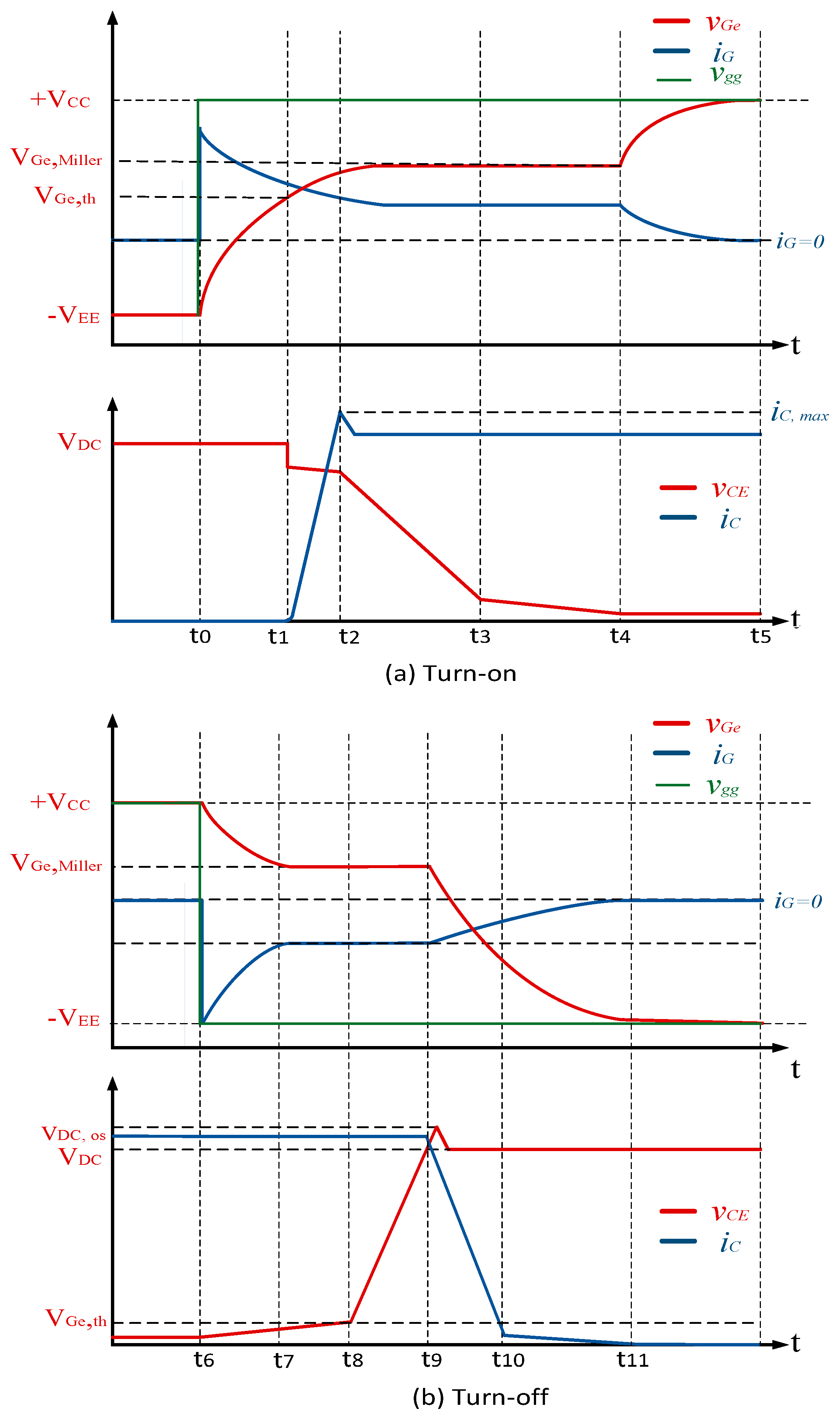
Figure 2.
(a) The test circuit and the proposed controller in the gate driver (GD). (b) General scheme of the controller.
Figure 2.
(a) The test circuit and the proposed controller in the gate driver (GD). (b) General scheme of the controller.

Figure 3.
Voltage type feedback signals originated from turn-on and turn-off switching transients and corresponding modified vgg.
Figure 3.
Voltage type feedback signals originated from turn-on and turn-off switching transients and corresponding modified vgg.

Figure 4.
(a) The collector current waveform, performed by the original gate driver. (b) The zoomed view to show the performance of the Active Gate Driver (AGD) with different Ki coefficient and its effect on the current at turn-on.
Figure 4.
(a) The collector current waveform, performed by the original gate driver. (b) The zoomed view to show the performance of the Active Gate Driver (AGD) with different Ki coefficient and its effect on the current at turn-on.

Figure 5.
(a) The waveform of collector-emitter voltage, performed by the original gate driver. (b) The zoomed view to show the performance of the AGD with different Ki coefficient and its effect on the voltage at turn-off.
Figure 5.
(a) The waveform of collector-emitter voltage, performed by the original gate driver. (b) The zoomed view to show the performance of the AGD with different Ki coefficient and its effect on the voltage at turn-off.

Figure 6.
The resultant iC from the closed-loop GD and conventional gate drive (CGD) at turn-on condition.
Figure 6.
The resultant iC from the closed-loop GD and conventional gate drive (CGD) at turn-on condition.
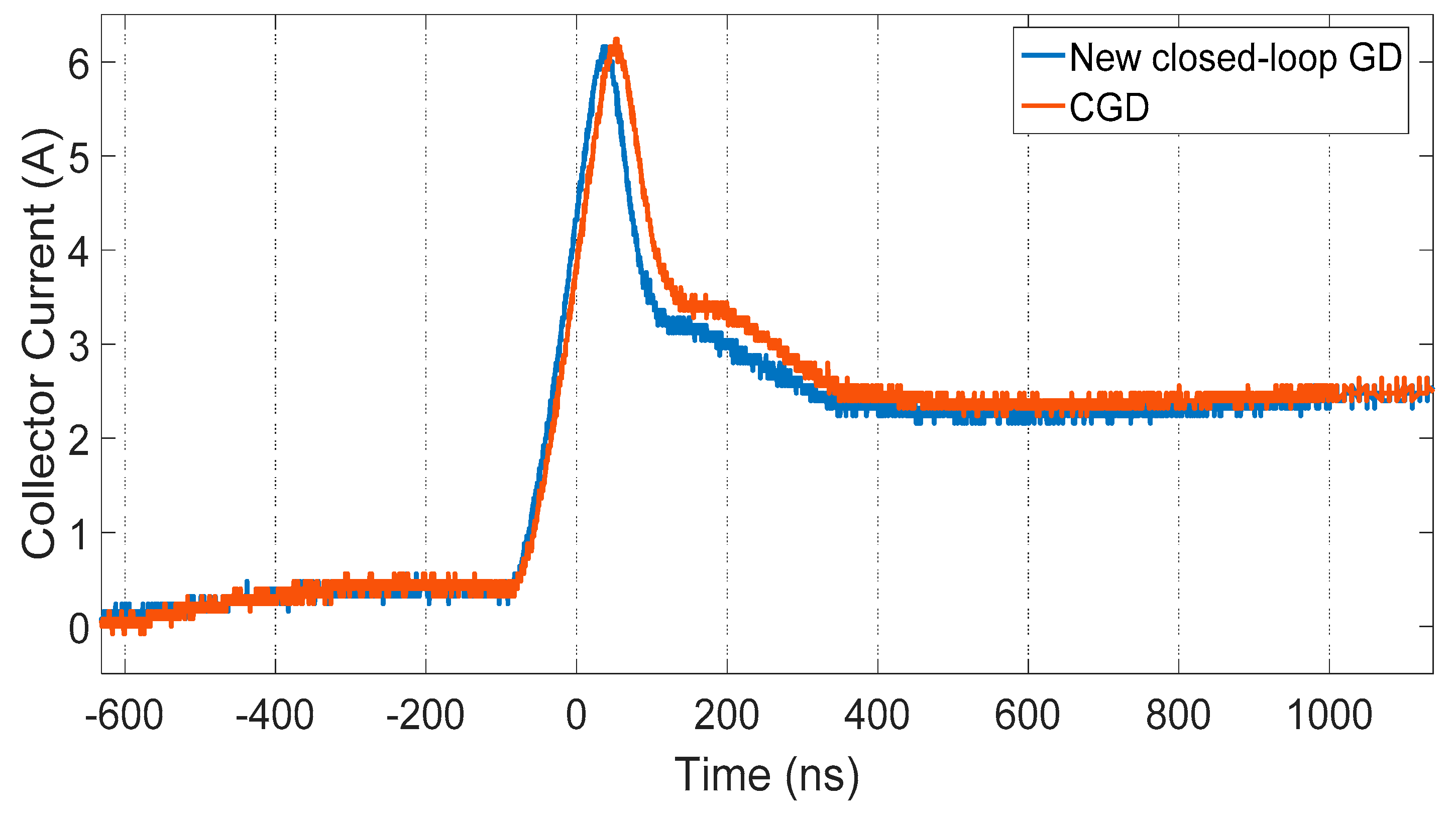
Figure 7.
The resultant vCE from closed-loop GD and CGD at turn-on condition.
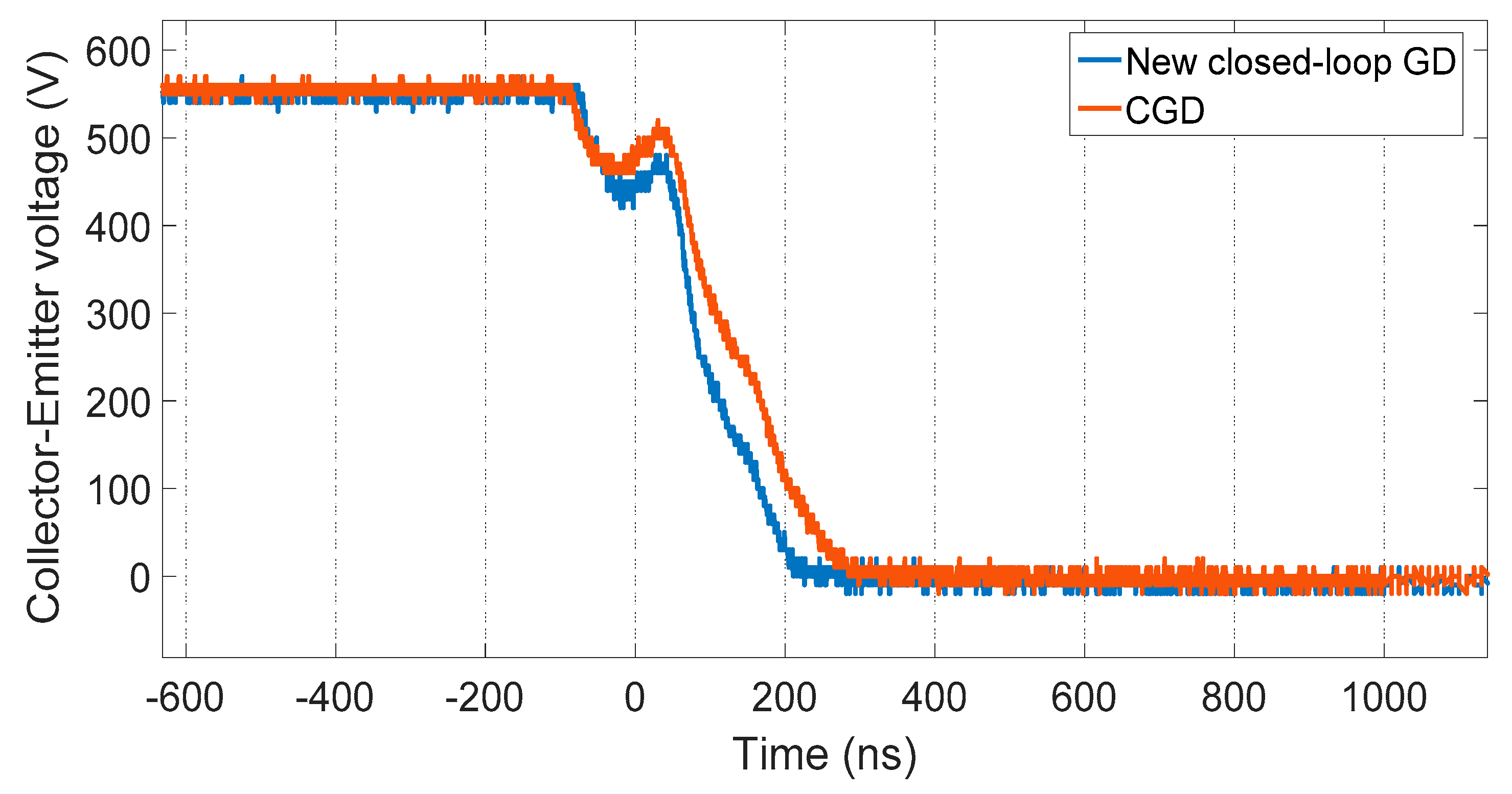
Figure 8.
The resultant VCE from closed-loop GD and CGD at turn-off condition.

Figure 9.
The resultant iC from the closed-loop GD and CGD at turn-off condition.

Figure 10.
The comparison of resultant spectrum between closed-loop GD and CGD with Rg = 12 Ω tested on VCE and iC experimentally. (a) Spectrum approximation of VCE and (b) spectrum approximation of IC.
Figure 10.
The comparison of resultant spectrum between closed-loop GD and CGD with Rg = 12 Ω tested on VCE and iC experimentally. (a) Spectrum approximation of VCE and (b) spectrum approximation of IC.


Table 1.
Collector current trajectory controlled by closed-loop GD with different Ki coefficients.
| Ki Coefficient | Intermediate Gate-Voltage Levels | diC/dt (pu.) | Over Current (pu.) |
|---|---|---|---|
| Ki1 | 6.8 | 0.54 | 0.77 |
| Ki2 | 7.6 | 0.58 | 0.8 |
| Ki3 | 8.4 | 0.65 | 0.85 |
| Ki4 | 9 | 0.69 | 0.9 |
| Original GD | - | 1 | 1 |
Table 2.
VCE trajectory controlled by closed-loop GD with different KV coefficients.
| Kv Coefficient | Intermediate Gate-Voltage Levels | dvCE/dt (pu.) | V-Overshoot (pu.) |
|---|---|---|---|
| Kv1 | 3.5 | 0.64 | 0.886 |
| Kv2 | 1.5 | 0.72 | 0.911 |
| Kv3 | -1 | 0.79 | 0.93 |
| Kv4 | -4 | 0.93 | 0.95 |
| Original GD | - | 1 | 1 |
Table 3.
The performance index.
| Gate Drivers | Overshoot Value in IC (A) | Overshoot Value in VCE (V) | Eon (µJ) | Eoff (µJ) |
|---|---|---|---|---|
| Original GD | 8 | 790 | 397 | 716 |
| New GD | 6.1 | 700 | 465 | 931 |
| CGD | 6.1 | 700 | 512 | 986 |
Table 4.
Cost and characteristic comparison.
| Drivers | Cost (pu) | Efficiency | EMI Reduction | Overshoot Reduction |
|---|---|---|---|---|
| GD+Snubber | 1 | Medium | High | High |
| Proposed AGD | 1.25 | High | High | High |
© 2019 by the authors. Licensee MDPI, Basel, Switzerland. This article is an open access article distributed under the terms and conditions of the Creative Commons Attribution (CC BY) license (http://creativecommons.org/licenses/by/4.0/).
Share and Cite
MDPI and ACS Style
Ghorbani, H.; Sala, V.; Paredes Camacho, A.; Romeral Martinez, J.L. A Simple Closed-Loop Active Gate Voltage Driver for Controlling diC/dt and dvCE/dt in IGBTs. Electronics 2019, 8, 144. https://doi.org/10.3390/electronics8020144
AMA Style
Ghorbani H, Sala V, Paredes Camacho A, Romeral Martinez JL. A Simple Closed-Loop Active Gate Voltage Driver for Controlling diC/dt and dvCE/dt in IGBTs. Electronics. 2019; 8(2):144. https://doi.org/10.3390/electronics8020144
Chicago/Turabian StyleGhorbani, Hamidreza, Vicent Sala, Alejandro Paredes Camacho, and Jose Luis Romeral Martinez. 2019. "A Simple Closed-Loop Active Gate Voltage Driver for Controlling diC/dt and dvCE/dt in IGBTs" Electronics 8, no. 2: 144. https://doi.org/10.3390/electronics8020144
Note that from the first issue of 2016, this journal uses article numbers instead of page numbers. See further details here.