A Software-Defined Radio for Future Wireless Communication Systems at 60 GHz


1
Instituto de Telecomunicações, 2411-901 Leiria, Portugal
2
Polytechnic Institute of Leiria, 2411-901 Leiria, Portugal
3
Department of Eletronics, Telecommunications and Informatics, University of Aveiro, 3810-193 Aveiro, Portugal
4
TWEVO Lda., 3030-199 Coimbra, Portugal
*
Author to whom correspondence should be addressed.
Electronics 2019, 8(12), 1490; https://doi.org/10.3390/electronics8121490
Submission received: 6 November 2019
/
Revised: 26 November 2019
/
Accepted: 3 December 2019
/
Published: 6 December 2019
(This article belongs to the Special Issue Millimeter-Wave (mmWave) Communications)
Abstract
:This paper reports on a complete end-to-end 5G mmWave testbed fully reconfigurable based on a FPGA architecture. The proposed system is composed of a baseband/low-IF processing unit, and a mmWave RF front-end at both TX/RX ends. In particular, the baseband unit design is based on a typical agile digital IF architecture, enabling on-the-fly modulations up to 256-QAM. The real-time 5G mmWave testbed, herein presented, adopts OFDM as the transmission scheme waveform, which was assessed OTA by considering the key performance indicators, namely EVM and BER. A detailed overview of system architecture is addressed together with the hardware considerations taken into account for the mmWave testbed development. Following this, it is demonstrated that the proposed testbed enables real-time multi-stream transmissions of UHD video content captured by nine individual cameras, which is in fact one of the killing applications for 5G.
1. Introduction
Millimeter wave (mmWave) communications are envisaged to be integrated in the upcoming generation of mobile networks, namely eMBB, one of the 5G verticals. This has been seen as the solution to increase the overall capacity of mobile radio cells, enabling the support of multi-Gigabit/s transmissions towards mobile equipments. Due to the large available bandwidth (55–66 GHz), mmWave band is, thus, very attractive for future 5G wireless communication systems, which might provide transmission data rates over 10 Gbps and network latency below 1 ms. However, even if a 2 GHz channel in the 60 GHz band is used to transmit data employing both 4 and 16-Quadrature Amplitude Modulation (QAM) modulations, data rate would still be limited to 4 and 8 Gbps, respectively. Therefore, there is demand for improving both system reliability and data rates. In this context, it is introduced in this work a novel software-define radio (SDR) mmWave testbed, aimed to tackle the 5G communication requirements outlined in [1].
With mmWave testbeds importance in mind, work at 60 GHz can be found in the literature [2,3,4]. However, such works were conducted with universal software radio peripheral (USRP) that offer limited bandwidths of around 25 MHz capabilities, which do not fulfill the 5G foreseen multi-Gigabits scenarios. To this extent, this work discusses the implementation of a real-time software-defined radio mmWave testbed that can cope with the next wireless generation needs.
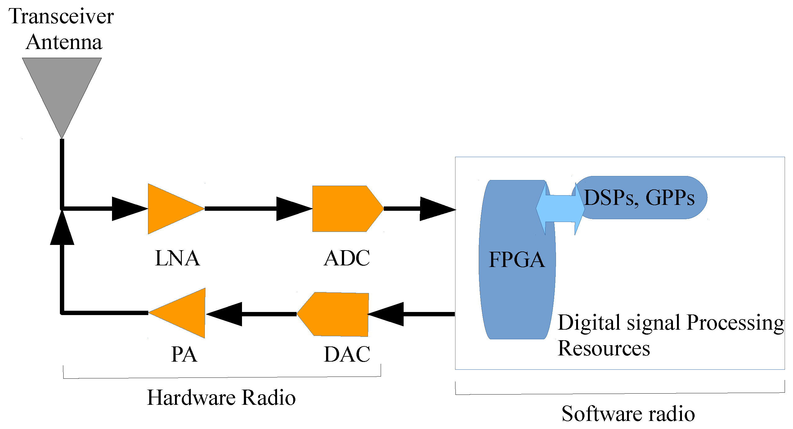
A software-defined radio (SDR) is a common term given to a system which employs the majority of physical layer functionalities using digital signal processing algorithms implemented in an embedded system with the aid of a specific software. In this context, typically, analog stages, such as mixing, amplification, filtering, modulators/demodulators, and essential to establish a wireless radio link, are digitally implemented rather than using discrete analog hardware components. Therefore, an ideal SDR is composed of very reduced hardware at the RF front-end, i.e., only an antenna and a very high speed sampler that is capable of capturing and digitizing a wideband radio signals [5]. However, relatively large coverage distances might only be attained by the employment of amplifiers prior to both DAC/ADC stages, as depicted in Figure 1. For example, at the receiver, a Low-Noise Amplifier (LNA) must be considered to reduce the converter quantization noise and thus maximize the Signal-to-Noise Ratio (SNR) at the digital domain (after sampling); only then is the signal converted to its binary form. Next, data are processed on a number of dedicated computational units, inside the embedded system, enabling the implementation of crucial methods for demodulation, synchronization, and decoding, which are required to recover the transmitted information from advanced modulation techniques.
Nevertheless, such architecture inherits the precision limitation from the digital domain representation, as well as it adds computation complexity to such digital domain. On the other hand, translating hardware discrete analog components functionalities into an embedded platform brings several advantages for a wireless communication system designer [7]:
- Design Flexibility: With the recent availability of very fast and accurate DACs/ADCs, traditional hardware circuitry such as filtering and analog modulators/demodulators can now be tuned.
- Reliability: In general, hardware component functionalities vary according to temperature, manufacturing variations, and ageing, which might lead to performance losses for the communication system. On the other hand, if such functionalities are implemented in a SDR platform, system’s performance is expected to remain the same over the years.
- Upgradability: Upgrading and improving a wireless system that is composed of only discrete components usually means replacing hardware, whereas using SDR a particular system might be upgraded without any additional cost, which lead to a more cost effective solution.
- Re-usability: Once a PHY is designed and tested in software, its deployment can be implemented in several hardware platforms.
- Reconfigurability: Current SDR implementations offers the capability of reconfigurable hardware to support several wireless standards and waveforms.
- Lower Cost: Fewer hardware components are necessary to be acquired in order to build a communication system from the scratch. Such devices are usually more expensive than the acquisition of SDR products.
A complete description of the developed SDR is outlined in Section 2, where special focus is given to the adopted firmware connectivity between the embedded system and both Giga Samples Per Second (GSPS) DAC/ADC boards. In addition, an extensive SDR characterization in terms of SNR, Spurious-Free Dynamic Range (SFDR), Signal-to-Noise and Distortion Ratio (SINAD), and Effective Number Of Bits (ENOB) is given, along with the proposed hardware design for Orthogonal Frequency Division Multiplexing (OFDM) systems based on the LTE-Advanced downlink PHY layer is given in Section 3. The OFDM performance in both Back-to-Back (B2B) and Over-The-Air (OTA) at 60 GHz scenarios was assessed in terms of Error Vector Magnitude (EVM) and the received scatter constellation plots for 4-/256-QAM. Finally, a showcase considering the proposed mmWave testbed with Ultra-High-Definition (UHD) multi-stream video, as usage case application, is outlined in Section 4.
2. 5G Testbed Overview
The proposed system was inspired on the previous Figure 1 and is composed of a baseband/low-Intermediate Frequency (IF) processing unit and a RF front-end at both TX/RX ends, as illustrated in Figure 2. In fact, it was the result of SDR OFDM integration with a RF front-end designed for mmWave. In Figure 2, it is evident that the low-IF waveform generation/demodulation is completely independent from the RF up-conversion/down-conversion. This modular approach was adopted to enhance the flexibility of the prototype radio system to enable signal transmissions at distinct frequency bands. That is, the mmWave carrier frequency can be tuned (to match other RF communication systems standards) by only changing the RF front-end.
This SDR system (Figure 2) is composed of an embedded platform engine called Field Programmable Gate Array (FPGA) [8], and at least by one pair DAC/ADC responsible for signal translation between the digital and analog domains. A FPGA is an integrated circuit intended for general purpose usage, which contains programmable logic blocks that form higher-level functions (multiplexers, adders, multipliers and RAM memories) and a reconfigurable interconnection between them [9].
FPGA platforms bring three main benefits for the designer: faster time-to-market (no layout for manufacturing needed), simpler design (the software handles much of the routing, placement, and timing) and re-programmability. Traditionally, all the above features would become available at the expense of chip performance, e.g., clock speed. However, in recent Xilinx’s FPGA technology digital clock values can now go over the 500 MHz performance barrier [9].
Consequently, FPGA technology was used for the 5G mmWave wireless communication that we propose especially due to their faster time-to-market and reduced cost characteristics. Due to its primal importance in this work, a brief overview of FPGA considerations is given in Section 2.1.
2.1. FPGA
One of the main challenges faced by embedded system developers is the diversity of external I/O interfacing requirements, which might be Ethernet, optical, analog conversion or Gigabit serial [10]. Thus, to enable data transfer between the embedded system and other hardware devices, the creation of external I/O interface is needed. Nowadays, FPGA come with one or more expansion slots for daughter boards (mezzanine module), which can increase the I/O possibilities. Such expansion slots allow FPGA designers to not rely solely on each FPGA I/Os and decrease system development costs. Without it, designers would need to change FPGA development board whenever system enhancements require additional interfaces [11].
To overcome this, the VITA 57 FPGA Mezzanine Card (FMC) connectivity ANSI/VITA standard was developed in 2008, to provide a modular standard mezzanine I/O interfacing solution to a FPGA located on a carrier board [11]. This brought several benefits such as maximum data throughput of 40 Gbps, low latency, reduced design complexity, and reduction of system cost [10].
Such standard foresees two types of expansion slots, also called FMC, which are usually populated on FPGA commercial solutions (LPC and HPC). While the first FMC solution has 160 pins, the second one has 400 available pins. Moreover, the Low Pin Count (LPC) connector provides 68/34 user-defined signals for single-ended and differential signals, respectively, as well as one serial transceiver pair, clocks, Joint Test Access Group (JTAG), and Inter-Integrated Circuit (I2C) interfaces. The High Pin Count (HPC) maintains precedent mentioned functionalities while providing twice the user-defined signals of the LPC connector also with 10 serial transceiver pairs.
At the time of this work, the most recent and powerful Xilinx FPGA (with more logic resources) available on the market is the Virtex FPGA’s family, namely Ultrascale [9]. For example, the XCVU9P-L2FLGA2104E chip provides more than 2000 k logic cells [12]. However, it is relatively expensive, and thus it was decided to acquire the Virtex-7 VC707 evaluation kit instead [13] (see Figure 3). This board is characterized as highly-flexible, having a high-speed serial XC7VX485T-2FFG1761C chip-set, and a good compromise between cost and available logical resources.
2.2. ADC/DAC
The selection of both DAC and ADC was based on the criteria of speed, bit resolution together with VC707 FPGA board compatibility. According to the Xilinx documentation, the FMC 230 (DAC) [14] and FMC 126 (ADC) [15] from 4DSP are the only converters available in the market that met such requirements. Table 1 summarizes the main converters features, where it can be noticed that the maximum bandwidth of the proposed SDR is restricted to 2.5 GHz.
The FMC126 is a four channel 1.25 GSPS 10-bit resolution ADC daughter board compliant to the mentioned HPC VITA 57.1 standard. Its design is based on four EV10AQ190 Quad 1.25 GSPS ADC chip-sets [18], which are characterized by Double Data Rate (DDR) Low Voltage Differential Signal (LVDS) outputs [16]. Moreover, each core can operate either individually, in pairs or even all interleaved together, which in the end enables sample rates of 1.25, 2.5, and 5 GSPS, respectively. To achieve the gigabit rates reported on this work, the ADC had its reference sample clock configured to 2.5 GHz, which can be locked by either an external clock source or an internal IC clock circuit.
The FMC230 is a two channel 14-bit DAC daughter board, which is controlled through a single Serial Peripheral Interface (SPI) communication bus [17]. Such board design is based on two AD9129 single-channel 14-bit 5.7 GSPS DAC with DDR LVDS inputs [19].
Since such boards are intended to work at gigabit rates, special attention was taken in their clock distribution. The clock distribution is carried out by a AD9517 chip from Analog Devices (AD) [20], which by default has an internal PLL and a 2500 MHz internal VCO. However, as discussed in Section 2.3, the VCO can also be provided externally.
As in FMC126, the FMC230 sample clock is provided by the mentioned AD9517, but its internal PLL reference is configured at MHz rather than 100 MHz, which in the end achieves an internal VCO locked at 2457.60 MHz (rather than the 2500 MHz).
2.3. ADC/DAC Integration with FPGA
The integration of ADC/DAC with VC707 board required hardware fine tuning to achieve the desirable data rates. Thus, this section addresses thoroughly the steps taken to achieve such integration. It is important to mention that 4DSP already offers a VC707 reference design to serve as basis, but multiple iterations were necessary to achieve the proposed mmWave SDR testbed.
Firstly, the reference design FMC slots were changed to have both boards working simultaneously using the same FPGA. Secondly, since both boards use FPGA Ethernet as an initialization and data interface, a physical connection had to be considered onto the proposed SDR testbed. Thirdly, sampling rate adjustments were performed, because both ADC/DAC had different default values which, in the end, would lead to loss of samples. Lastly, both DAC and ADC data path were changed to be transmitted in real-time rather than using the default memory architecture, which temporarily allocates data in memories before transmission.
As mentioned above, 4DSP reference firmwares target Ethernet communication as the protocol to perform the initialization of both devices and to transmit/receive data. Consequently, such architecture demands a host PC to be always connected to the FPGA, which is impractical in a wireless communication transceiver. Therefore, Ethernet connection must be replaced by a new VHDL entity capable to play back initialization commands that were previously sent by the MAC engine to the FMC board entities (). This approach is highlighted in the block diagram illustrated in Figure 4, where all the connections in red are the ones that must be removed from the original FMC230 and FMC126 reference designs. With such changes, the MAC engine star is now just considered to generate clock and reset signals to the others stars and, due to this fact, it has been decided not to be removed.
In this work, the aforementioned new entity is a processor engine, which allows the configuration commands of both converters to be sent (in real-time) from the FPGA to either ADC or DAC. Nevertheless, the design and implementation of a processor hardware engine architecture is not a straightforward task. It is usually composed of a microBlaze processor, peripherals, reset, clocking and debugging blocks, which are connected together using an AXI4-Stream protocol [21]. Since the microBlaze is a soft-core processor with 32-bit RISC architecture and AXI interfaces, the developed entity had AXI in mind for easy, direct access to fabric and hardware acceleration [22]. It is worth noting that this interface/protocol is not a bus, and thus a custom user block was necessary to convert the AXI data coming from the processor engine to the bus format given in Figure 4.
The VC707 board has two instances of the FMC HPC VITA 57.1 mentioned in Section 2.1. However, the VC707’s HPC2 connector is not fully populated, e.g., it has a reduced pin-out in comparison with the standard HPC connector. Consequently, the FMC230 placed on such connector would only have one out of its two DAC channels available. On the other hand, if FMC126 would be connected to it, only three out of its four ADC channels could be available. Considering that most relevant modern digital modulation techniques employ I/Q modulations to achieve higher spectral efficiency, two channels are required in both DAC/ADC boards. Therefore, FMC230 and FMC126 have been connected to the FMC1 and FMC2 slots of the VC707 board, respectively, as can be seen in Figure 3.
Figure 5 depicts the final firmware that shows how the configuration commands are exchanged among the top level board entity (stars) from both DAC/ADC boards.
The FMC126 board includes not only the Quad ADC IC core itself, but also other peripherals, such as a clock tree IC circuit and a I2C communication for ADC control purposes and temperature monitoring [16]. Since the FMC126 reference design foresees its use in the HPC1 connector, the I2C clock () and data () signals must now be driven to the second HPC2 connector. This can be achieved by changing VC707’s I2C switch, PCA9548A [23]. As depicted in Figure 6, the entity should route signals either to FMC1 or FMC2 connectors depending on I2C channel selection.
2.4. ADC/DAC Sample Rate Synchronisation
With both ADC/DAC fully integrated in VC707 FPGA, considerations on their data sampling process was studied and addressed. Such process at the receiver might be subject to severe timing imperfections such as erroneous information acquisition or transmitted samples loss depending on both DAC/ADC sampling rates difference [5]. The erroneous information acquisition can occur when ADC rate is higher than DAC, whereas loss of transmitted samples might happen if ADC rate is lower than DAC. That said, sampling rate of both converter boards considered should match.
The easiest solution, found in this work, to meet the above requirement is to configure the clock tree of the FMC230 to drive a 1.25 GHz clock signal into both AD9129 cores. This would be a very straightforward task if the internal VCO of the AD9517-1 could generate a 1.25 GHz operating frequency (maximum rate achievable by FMC126 without phase interleaving) or integer multiples of this frequency. In Figure 7, it is seen that the DAC sample clock, driven by the path, is provided by the output of AD9517-1. This port provides clock frequencies from 2457.6 MHz down to 12.8 MHz, which are the result of configuring either both block divisors and or, alternatively, bypassing and using , or vice versa. However, only integer values are acceptable in such block dividers, and, thus, is not possible to obtain a divisor combination where port is at 1.25 GHz. Therefore, meeting the ADC sample clock in the FMC230 is only possible considering an external signal as sample clock reference.
As a workaround, the clock tree of the FMC126 has been configured to enable a Clock Output (CO) signal, with Low-Voltage Positive-referenced Emitter Coupled Logic (LVPECL) waveform type, at 1.25 GHz, to be connected to the Clock Input (CI) port of FMC230. Although the AD9517-3 circuit can be easily configured to enable as CO, this port is not connected to any external connector in the FMC126 board. To overcome this, an additional SSMC connector has been soldered to the CO port pad in the reverse side of the device PCB.
2.5. FMC126/FMC230 Data Interface
It is well known that operating FPGA logic at GHz clock frequencies is impractical, since very low rising interval times result into failing design timing requirements and data integrity is not ensured. Looking at current solutions, the FPGA clock performance barrier is around the 500 MHz. Hence, 4DSP adopted a parallel data path architecture in both original FMC230/FMC126 firmwares, which reduces significantly the required data clock frequencies to MHz. For example, from the FMC230 functional block diagram (see Figure 7), two parallel data DDR interface paths come from the FMC connector ( and —operating at ), and are then multiplexed into a single data stream by the assembler entity, which is clocked at , where represents the DAC sampling rate value ().
A detailed block diagram of the FPGA data connectivity with DAC’s firmware is depicted in Figure 8. In the figure, it is verified that data source is generated in the entity, driven by the bus signal (16 words of 16bits each) clocked at . Such clock value is equal to value divided by 4 or DAC . Since AD9129 bit resolution is 14 bits, the two most significant bits are then discard in the entity. In this entity, the 256 data bit bus () is serialised, using two sets of fourteen parallel to serial structures of Oserdeses2 (high-speed source-synchronous output fabric interfaces) operating in DDR mode. This results in two buses of 14 bits ( and ), clocked at clock, which are then connected to the FMC230 board through the FMC1 pin-out connection (see Figure 7).
The data interface of the FMC126 with FPGA is rather similar to the FMC230 ones, but here eight parallel data paths are considered instead. That is, data go to the FMC230 on a 256 bit bus, whereas data come from the FMC126 on a 128 bit bus. This leads to a mismatch of the clock value in both DAC and ADC firmware channel paths. For example, considering a target sampling rate of 1.25 GHz, buses are clocked at 78.125 MHz and at 156.25 MHz for FMC230 and FMC126, respectively. To overcome this issue, the number of data paths in the FMC230 firmware were reduced to 8 (matching the ones from the FM126), and thus entities, namely, , , and , have been updated accordingly, where value is now given by = .
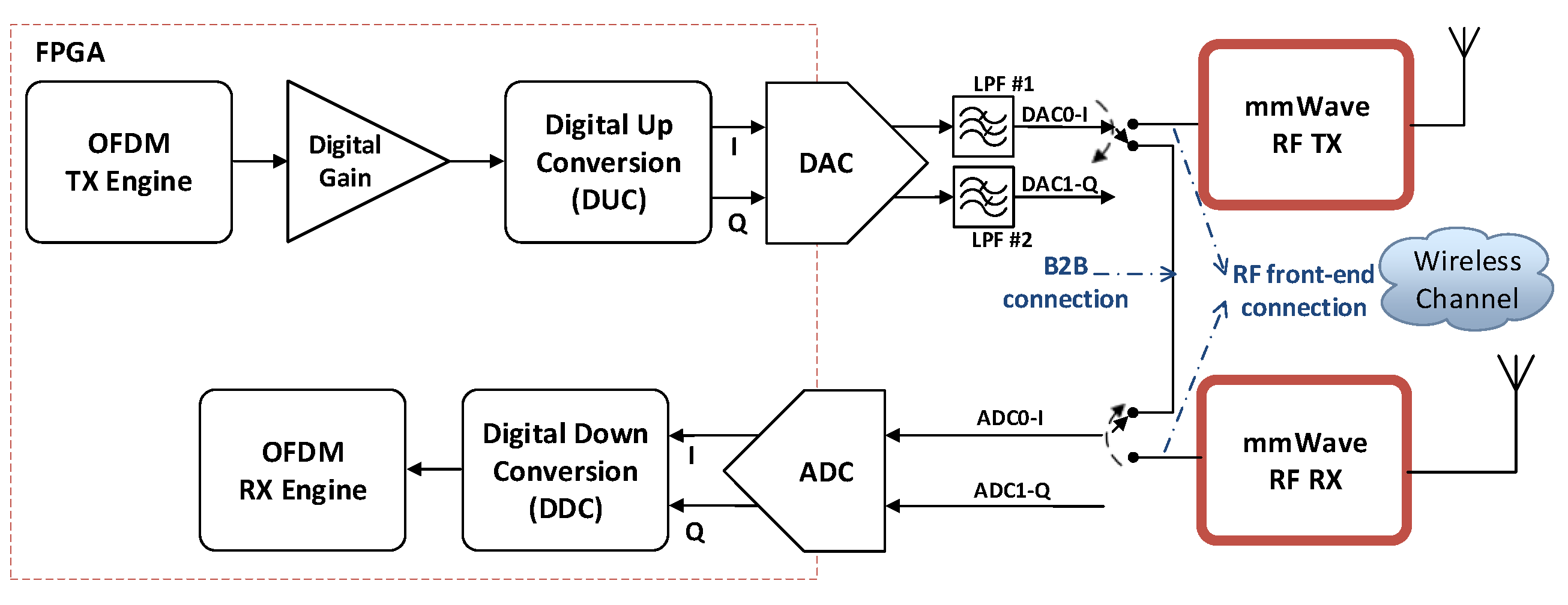
The proposed communication transceiver prototype is based on the digital IF architecture shown in Figure 9. Such architecture offers more flexibility when compared to traditional RF architectures, and is not sensitive to DC offset, LO leakage and flicker noise. Moreover, since I/Q up-conversion/down-conversion is digitally performed in an IF stage, negative effects induced by IQ imbalances, critical in advanced modulation techniques, are therefore limited. Note that both Digital Up-Conversion (DUC) and Digital Down-Conversion (DDC) stages are performed to relatively low center IF frequencies (limited by the sampling rate of both DAC/ADC); however, up-conversions to mmWave can be accomplished by an external analog mixer, as discussed in Section 2.6.
As previously stated, the testbed data source is modulated with a real-time OFDM Transceiver (TRX) engine, which was developed in Xilinx System Generator (SysGen) environment. SysGen is the state-of-the-art tool for the design, testing, and implementation of high-performance DSP algorithms on FPGAs. It enables a rapid prototyping of very complex FPGA design by considering the Mathworks model-based design environment, namely Simulink, with total abstraction of the chip-set complexity [24,25]. In this context, OFDM TRX engine (testbed) was packed in SysGen into a customized IP to be integrated into the previously discussed transceiver firmware.
However, to design and implement the aforementioned communication system, it is required to understand how a real-time data source engine would be integrated to the data interface of both ADC/DAC reference designs (eight parallel processing paths at 156.25 MHz). In this context, at the transmitter, a DSP interpolation filter is necessary, which would be capable of interpolating the sample rate of 156 MHz to the DAC sampling rate of 1.25 GHz. Such solution was implemented using Finite Impulse Response (FIR) filter banks (clocked at 156.25 MHz) by following the polyphase decomposition algorithm reported in [26]. This solution increases the sampling rate and attenuates the generated spectral images from the up-sampling process using a low-pass filter, which also shapes the transmitted signal bandwidth [5]. On the other hand, on the RX side, the counter part must be implemented. That is, ADC sampling rate is decreased using a down-sampling operation followed by a low-pass filter, removing undesired components that would otherwise overlap (aliasing) into the used band. These two operations together result in a decimation filter [5]. It is worth noting that for the I/Q up-/down- conversion 16 distributed FIR filters are necessary.
A filter bank is characterized by a parallel arrangement of low-, band-, or high-pass filters, required to decompose the spectral content of a certain signal into multiple sub-bands [27]. When the filter bank is implemented based on a low-pass prototype filter, which corresponds to the 0th band, the other uniform sub-bands are obtained by frequency shifting the prototype filter frequency response [28]. In this case, it is known as DFT filter bank and the graphical representation of its frequency response is illustrated in Figure 10.
Furthermore, the polyphase decomposition algorithm [26] can be employed to enable an efficient real-time implementation of uniform filter banks, while ensuring the perfect-reconstruction of the analysis/synthesis process.
Since eight parallel signal processing paths are required per I/Q path, eight analysis/synthesis FIR filters were carefully designed and implemented, considering the following procedure:
- Filter response type: It is well known that pulse shaping with raised cosine is characterized by a zero-Inter-Symbol Interference (ISI) [5]. That is, despite its impulse response extending over several other symbol periods, at the decision points, there is neither constructive nor destructive interference. Therefore, in this work, a square root raised cosine matched filter pair was considered, which have the same zero-ISI properties of the raised cosine [5].
- Filter order and frequency specifications: The interpolation/decimation filter was designed with the aid of the Matlab FDAtool algorithm. In this tool, the normalized LPF cut-off bandwidth was set to 0.125, which is the relation between the clock rates of a single processing path and the DAC core. Moreover, both Kaiser window Beta, and filter roll-off values were set to 2 and 0.25, respectively, since this configuration was found to be the best compromise between passband ripple, stop-band attenuation, and transition band. Finally, filter order was chosen to be 62, since it was also a compromise among system complexity, stop-band attenuation, and transition band.
- Distributed implementation of interpolation/decimation: Both filter banks were implemented using multiple parallel FIR digital filters.
Additionally, both IQ up-/down- conversion stages can be performed by the multiplication of the desired signal by a complex exponential operating at a certain center frequency (), as it is illustrated in Figure 9. At the transmitter, the baseband signal spectrum is frequency shifted to be centered at (), resulting in a non-symmetric spectra [5]. Consequently, applying at the receiver, will move the transmitted signal spectra to be centered at DC, thus converting the received signal back to baseband.
Such complex exponential function was implemented using a Coordinate Rotational Digital Computer (CORDIC) DSP algorithm, which is responsible for implementing an IQ-mixer with angular frequency proportional to the desired value. However, since both DAC/ADC converters employ an eight parallel processing path technique, similar to the FIR filter introduced above, a distributed CORDIC with eight paths operating at 156 MHz is also required to perform either an up-conversion or down-conversion. To this end, the distributed CORDIC must generate samples of the same complex exponential but at shifted sample instants in each processing path. It is worth noting that each CORDIC path in the TX FPGA firmware should be connected to the parallel structure of OSERDES, in order to perform the data serialization required in the data interface of the FMC230. In the RX firmware, to shift the signal back to baseband, a similar distributed CORDIC approach was employed but with negative phase increment. Then, it was connected to a parallel structure of ISERDES, which enables data parallelism and consequently reduction of the data clock.
Finally, to integrate the developed SysGen OFDM with the transceiver firmware, it was necessary to package and export such modulation into two distinct TX/RX IP customized blocks. That can be seen in the high-level block diagram illustrated in Figure 11.
2.6. RF Front-End Overview
With both ADC/DAC integration in FPGA and OFDM engine working seamlessly, this work next step was to develop the mmWave RF front-ends. The used front-end is a fully custom-made solution composed by several analog components connectorized, as illustrated in Figure 12 and Figure 13.
On the transmitter side, it was considered a typical direct-conversion (to avoid IQ imbalance effects on transmitted signals) also known as homodyne architecture (see Figure 12). It is composed of a PLL operating at 15 GHz, a multiplier by 4, which up-converts the LO signal to 60 GHz, and an up-conversion mixer. In addition, an external 10 MHz reference clock is required for the PLL. In addition, to avoid the non-linearities introduced by the Power Amplifier (PA), the amplification stage at RF (60 GHz) has deliberatively not been included in this study. Otherwise, it would have required the study of mitigation techniques such as Digital Pre-Distortion (DPD).
At the receiver, a two-stage heterodyne architecture is employed. A Low-Noise Amplifier (LNA) at RF is coupled to the antenna, followed by a down-conversion to a 6 GHz IF stage, performed by a first mixing stage process with a 54 GHz LO signal. In a second down-conversion stage, received signals are shifted to IF frequencies. Therefore, unlike the transmission architecture, two PLLs operating at 13.5 and 6 GHz are therefore required, as can be seen in Figure 13. Furthermore, the external clock references for both TX/RX PLLs are generated by two independent PRS10M rubidium oscillator. Such reference clock signals are characterized by very low phase noise and very high frequency stability (≈0.05 ppb), being, therefore, very reliable clock sources.
3. Results Discussion
In this section, three sets of measurements are reported and analyzed. In particular, focus on the performance of ADC/DAC integration in FPGA is given. Then, performance comparison of different IF frequencies using the mentioned SDR system with OFDM engine is conducted. In the end, the proposed system (mmWave 5G testbed) performance is addressed with EVM and received scatter constellation analysis.
3.1. ADC/DAC Characterization
The FMC126 and FMC230 boards with their design modifications were characterized and validated with the usual figures of merit such as SINAD, ENOB and SFDR metrics.
With that in mind, an oscilloscope and a Spectrum Analyzer (SA) were used to measure the time and frequency responses of the DAC at multiple tones. With regards to the ADC, a signal generator was used to generate sine-wave signals with tuneable amplitude and frequency, which allowed both time and frequency responses assessment.
The DAC performance assessment was evaluated with the DAC’s SFDR, which is measured as the difference between RMS power level of the transmitted tone and the most significant spur signal, presented in the DAC’s frequency response. The SFDR measurement result, for the FMC230, can be seen in Figure 14 considering the D1 channel and a frequency tone of 134.3 MHz.
Additionally, the FMC230 was also characterized with SINAD, SFDR, and ENOB figures of merit for various frequency tones. Such results are summarized in Table 2 and plotted in Figure 15a,b, considering a sampling rate of 2456 MHz and DAC’s D1 output channel. The average values for SFDR, SINAD, and ENOB measurements are 56.93 dB, 69.61 dB, and 11.34 bits, respectively, which according to 4DSP datasheet is within DAC performance boundaries.
With FMC126 in mind, a similar experimental setup was used to assert this ADC board performance. Consequently, the reference signal connected into both ADC’s channel A and B, was characterized with 72.5 dB of SFDR, which is limited by the SNR of the considered signal generator equipment (Figure 16a), for a signal power level of −2 dBm (ADC full-scale input value).
Moreover, comparing Figure 16a,b, it is verified that ADC sampling and quantization processes induce a performance degradation of 12.7 dB in terms of SFDR, leading to a maximum dynamic range of 59.8 dB.
3.2. Back-to-Back Performance
Following the ADC/DAC assessment, measurements with baseband integration were conducted. It is important to mention that, following the 5G pre-trials specification presented in [1], a multi-Gigabit/s real-time OFDM TRX engine was developed [29]. Such OFDM baseband engine architecture is extensively discussed in [29] and was based on the previous work reported in [30]. Such engine enhancements led to a 1 Gbps real-time transmission rate (considering 256-QAM), which fullfills next wireless generation requirements. That said, the considered OFDM main design operating parameters, particularly the FFT and data size block values are given in Table 3.
Table 4 outlines the main SDR system specifications accomplished by integrating both OFDM modulator/demodulator, with the digital IF architecture using the disruptive modular fully pipelined hardware architecture illustrated in Figure 11.
Firstly, the TRX performance of such SDR was evaluated in B2B configuration using EVM as QoS assessment metric. In Figure 17, an example of the transmitted OFDM signal spectrum was obtained considering a frequency centered at 312.5 MHz (IF4) and selected digital gain of 7.
Additionally, numerous OFDM IF possibilities were considered, such as zero IF (DC), IF2 (156.25 MHz), IF4 (312.5 MHz), and IF6 (468.75 MHz). Figure 18 shows the output power transfer curve as a function of the selected gain and IF modulations. It was verified that OFDM modulation centered at IF2 has less signal attenuation than the remaining IF frequencies, leading to higher DAC output power.
In Table 5, the EVM results are summarized for the maximum digital gain of 7 using four different IF configurations. Additionally, when either I or Q channels are used to transmit and receive data, EVM results are denoted or , respectively. That is, connecting DAC0 to ADC0 is considered as the , and connecting DAC1 to ADC1 channels is the . Additionally, for a quadrature transmission, both I/Q channel branches are used simultaneously. These results show that a minimum EVM of approximately dB is obtained for all low IF modulations, except for zero-IF, in which synchronization algorithms fail to estimate the beginning of frame, due to the nulls obtained on both DAC/ADC frequency responses. As expected, for other IFs, no OFDM performance degradation is verified, even when an IQ transmission configuration is considered, indicating that very low distortion is present on received signal constellations.
Finally, in Figure 19, it can be seen that the 4- and 256-QAM constellations do not present significant scattering distortion on the received symbols, by using IF2 frequency and a maximum digital gain. This subjective quality evaluation indicates that the OFDM SDR system is thus very accurate.
3.3. OTA 60 GHz Performance
Now, the effect of RF impairments on the quality of TRX OFDM system, outlined in Section 3.2, is addressed with 60 GHz over-the-air measurements under different conditions of RX SNIR and employed modulations. With possible OFDM performance degradation due to multipath effect in mind, the testbed was firstly set inside an anechoic chamber under LOS condition. With such controlled environment, it is possible to accurately assess the RF front-end impact on the previously discussed OFDM communication system. The system QoS was assessed through EVM figure of merit and spectral efficiency per stream analysis. In the end, testbed results with 25 dBi antennas show a maximum distance range of cm.
A Bit Error Rate (BER) estimation was accomplished by using the relation between this metric and EVM, given in Table 6 [30]. The EVM results were computed for each OFDM IF modulated signal under different SNIR in either the presence or absence of CFO. For example, Table 7 shows the measured average EVM values for an IF OFDM modulated signal at 312.5 MHz (IF4). The minimum average EVM value, dB, is verified for an input power of dBm when both TX/RX devices are clocked using different sources. Such value together with Table 6 indicates that the RF front-end can handle QAM modulations up to 256-QAM, meaning that 1 Gbps of data transmissions are possible with the proposed mmWave testbed.
For quality assessment of the proposed testbed the EVM value, 4-, 16-, 64-, and 256-QAM received constellations, are depicted in Figure 20a–d, respectively. These results present a slight scattering distortion on the received symbols when compared with the B2B configuration (see constellations of Figure 19). However, even for 256-QAM, all constellations exhibit a well defined point scattering area, which indicates a low probability of decoding erroneous bits.
Furthermore, Table 8 shows the minimum average EVM and its degradation for the remaining IF OFDM modulations. For IF values of 312.5 and 468.75 MHz, EVM is below 3%, representing a performance degradation below 2% when compared to a back-to-back configuration. This is quite remarkable, since the EVM values at 60 GHz are lower than the 2.5% required by sub-6 GHz Wi-Fi (IEEE 802.11.ac) to employ 256-QAM OFDM transmissions [31]. To the best of authors’ knowledge, this spectral efficiency per stream and SNR results go significantly beyond the state-of-the-art, when compared to the current mmWave testbeds. Finally, for the proposed link budget the received power versus digital modulation, for an BER of , is presented in Table 9.
Finally, in Figure 21, it is shown the input power operating range of the mmWave RF front-end considering IF4. It can be seen that such system operates with a relatively wide input dynamic power range considering an EVM threshold of dB, which is enough for a error-free QPSK demodulation.
From the above results, it is demonstrated that it is possible to successfully use the mmWave spectrum to achieve multi-Gigabit/s, while considering relatively high spectral efficient modulations, and signal bandwidths greater than 100 MHz. For example, in literature only the 28 GHz testbeds reported in [32,33,34,35], consider a modulation bandwidth higher than 100 MHz using real-time baseband processing, and considering the 5G NR waveform as the transmission scheme (OFDM). On the other hand, at 60 GHz, it is evident a lack of testbeds that comply the minimum technical performance requirements of IMT 2020 for 5G. Considering the proposed OFDM testbed, the 5G peak spectral efficiency value of 7.8 bit/s/Hz [1] was achieved, and thus, the gap verified in testbeds operating at 60 GHz has been fulfilled. In other words, no other prototype system can process a signal BW of 150 MHz in real-time with modulation orders up to 256 QAM, using OFDM as transmission scheme in an over-the-air scenario. It is worth noting that even the listed 28 GHz testbed systems, do not meet the DL specification of 7.8 bit/s/Hz.
4. Showcasing: From GbE-Based to UHD Multi-Stream Video
In order to make the testbed appealing to the general public, a video base demonstrator was put together, as it is depicted Figure 22. Such showcase was a joint-collaboration with the Multimedia group in IT Leiria that developed a 180 field of view system as in [36].
The UHD multi-stream showcase has been presented at several key forums, creating great impact with both scientific community and industrialist. Such video content was generated independently with the 180 field of view camera setup [36], which is composed of 9 UHD cameras responsible for 20 video acquisition each. Due to the agglomerate high data throughput, a GigabitEthernet connection is required to route all 9 UHD cameras data from the encoded stream outputted from the Raspberry Pi to the transmitting FPGA. That said, a GbE switch merges all 9 Raspberry Pi ethernet connections into the single GbE available at TX baseband unit. At RX side, a high performance laptop with GbE interface runs VLC for real-time decoding and video displaying, the decoded video content from the RX baseband unit.
This has proven to be eye-catching and intuitive, since the visitors could directly interact with the system, e.g., by blocking the direct radio path and observe the immediate impact in both received signal constellations and received video quality. Such user interaction coupled to the fact that 9 UHD video streams were being displayed in real-time on the computer, provided the required validation of a real-time over-the-air user experience. On the other hand, for those with a technical background, there is a Graphical User Interface (GUI) displaying in real-time the received signal constellation, as well as the estimated BER values.
5. Conclusions
In this article, a novel software-defined radio solution for future wireless communication systems is presented and validated as a complete multi-Gigabit/s radio in-the-loop OFDM transmission scheme with mmWave 60GHz RF front-end to cope with UHD multi-streams.
The SDR hardware choice was based on the overall criteria of low time-to-market and reduced development costs. On the one hand, VC707 FPGA was the choice for the embedded DSP engine, since at that time it was the best compromise among available logic resources, highly-flexible, high-speed serial bus I/O interface, and cost. In addition, both FMC230/FMC126 were selected based on their inherent high sampling rates, bit resolution, and their compatibility with the VC707 FMC I/O interface connectivity.
Moreover, firmware connectivity issues between the embedded system and both FMC230/FMC126 have been outlined in this work, as well as the considered workarounds to enable a GSPS real-time communication system. Currently, the SDR is configured to 1.25 GSPS, which, as discussed, is 5G future-proof. In addition, both ADC/DAC converters were deeply characterized in terms of SNR, ENOB, SINAD, and SFDR, and their advantages of a digital IF RF architecture has been extensively discussed.
Additionally, a complete multi-Gigabit/s radio in-the-loop OFDM communication system was implemented for high data rate applications considering 4-, 16-, 64-, and 256-QAM, which was validated. EVM results in both scenarios were below 2%, which is quite remarkable considering the current norm for employed 256-QAM OFDM transmissions is 2.5% [31].
A complete overview on mmWave front-end was done, which together with the baseband unit form a robust communication system with rates up to 1 Gbps. The chosen use case for this work was UHD video stream that was achieved with a 180 field of view setup available at IT.
In summary, this work details the required steps to achieve a real-time testbed that meets 5G requirements on the mmWave frequency range with 1 Gbps and low latency main characteristics.
Author Contributions
Conceptualization, methodology, software, validation, formal analysis, investigation, resources, data curation, writing—original draft preparation, writing—review and editing and visualization—L.D., R.G., C.R. and R.F.S.C.; Supervision, project administration and funding acquisition—C.R. and R.F.S.C.
Funding
This research was partially supported by the Portuguese Government under the project RETIOT—Reflectometry Technologies to Enhance the Future Internet of Things and Cyber-Physical Systems, reference POCI-01-0145-FEDER-016432 (SAICT-45- 2015-03/16432), funded by FEDER within COMPETE 2020; Instituto de Telecomunicações under the projects 5G TESTBED and 5G MIMO TESTBED (UID/EEA/50008/2019).
Conflicts of Interest
The authors declare no conflict of interest.
References
- Shafi, M.; Molisch, A.F.; Smith, P.J.; Haustein, T.; Zhu, P.; Silva, P.D.; Tufvesson, F.; Benjebbour, A.; Wunder, G. 5G:A Tutorial Overview of Standards, Trials, Challenges, Deployment, and Practice. IEEE J. Sel. Areas Commun. 2017, 35, 1201–1221. [Google Scholar] [CrossRef]
- Quadri, A.; Zeng, H.; Hou, Y.T. A Real-Time mmWave Communication Testbed with Phase Noise Cancellation. In Proceedings of the IEEE INFOCOM 2019—IEEE Conference on Computer Communications Workshops (INFOCOM WKSHPS), Paris, France, 29 April–2 May 2019; pp. 455–460. [Google Scholar] [CrossRef] [Green Version]
- Zetterberg, P.; Fardi, R. Open Source SDR Frontend and Measurements for 60-GHz Wireless Experimentation. IEEE Access 2015, 3, 445–456. [Google Scholar] [CrossRef]
- Saha, S.K.; Ghasempour, Y.; Haider, M.K.; Siddiqui, T.; Melo, P.D.; Somanchi, N.; Zakrajsek, L.; Singh, A.; Shyamsunder, R.; Torres, O.; et al. X60: A Programmable Testbed for Wideband 60 GHz WLANs with Phased Arrays. Comput. Commun. 2019, 133, 77–88. [Google Scholar] [CrossRef]
- Stewart, R.W.; Barlee, K.W.; Atkinson, D.S.W.; Crockett, L.H. Software Defined Radio Using MATLAB & Simulink and the RTL-SDR; Strathclyde Academic Media: Glasgow, UK, 2015. [Google Scholar]
- Bronckers, S.; Roc’h, A.; Smolders, B. Wireless Receiver Architectures Towards 5G: Where Are We? IEEE Circuits Syst. Mag. 2017, 17, 6–16. [Google Scholar] [CrossRef] [Green Version]
- Software-Defined Radio. Available online: https://www.winradio.com/home/facts.htm (accessed on 18 October 2017).
- Kuon, I.; Rose, J. Measuring the Gap Between FPGAs and ASICs. IEEE Trans. Comput. Des. Integr. Circuits Syst. 2007, 26, 203–215. [Google Scholar] [CrossRef] [Green Version]
- Field Programmable Gate Array (FPGA). Available online: https://www.xilinx.com/products/silicon-devices/fpga/what-is-an-fpga.html (accessed on 8 March 2017).
- Malachy Devlin. VITA 57 (FMC) opens the I/O pipe to FPGAs; Forasach: Glasgow, UK, 2012. [Google Scholar]
- Paper, W. I/O Design Flexibility with the FPGA Megazzine Card (FMC); Technical Report; Xilinx: San Jose, CA, USA, 2009. [Google Scholar]
- Xilinx Ultrascale. Available online: https://www.xilinx.com/support/documentation/selection-guides/ultrascale-plus-fpga-product-selection-guide.pdf (accessed on 6 November 2019).
- Xilinx VC707. Available online: https://www.xilinx.com/products/boards-and-kits/ek-v7-vc707-g.html (accessed on 6 November 2019).
- 4DSP FMC126. Available online: http://www.4dsp.com/{FMC}126.php (accessed on 6 November 2019).
- 4DSP FMC230. Available online: http://www.4dsp.com/{FMC}230.php (accessed on 6 November 2019).
- UM009 FMC12x. FMC122/FMC125/FMC126: User Manual; Technical Report; 4DSP: Austin, TX, USA, 2014. [Google Scholar]
- UM023 FMC230. FMC230: User Manual; Technical Report; 4DSP: Austin, TX, USA, 2015. [Google Scholar]
- EV10AQ190 Datasheet. Available online: https://www.teledyne-e2v.com/resources/account/download-datasheet/1735 (accessed on 8 January 2017).
- AD9129. 11-/14-Bit, 5.7 GSPS, RF Digital-to-Analog Converter; Data Sheet; Analog Devices: Norwood, MA, USA, 2017. [Google Scholar]
- AD9517. 12-Output Clock Generator with Integrated 2.8 GHz VCO; Data Sheet; Analog Devices: Norwood, MA, USA, 2013. [Google Scholar]
- UG940. Vivado Design Suite Tutorial: Embedded Processor Hardware Design; Technical Report; Xilinx: San Jose, CA, USA, 2017. [Google Scholar]
- UG761. AXI Reference Guide; Technical Report; Xilinx: San Jose, CA, USA, 2011. [Google Scholar]
- PCA9548A. Low Voltage 8-Channel I2C Switch with Reset; Technical Report; Texas Instruments: Dallas, TX, USA, 2015. [Google Scholar]
- Mittal, S.; Gupta, S.; Dasgupta, S. System Generator: The State-of-art FPGA Design tool for DSP Applications. Proceedings of Third International Innovative Conference On Embedded Systems, Mobile Communication And Computing (ICEMC2 2008), Pesimsr, India, 11–14 August 2008. [Google Scholar]
- Paper, W. Model-Based Design with Simulink, and Xilinx System Generator for DSP; Technical Report; MathWorks: Natick, MA, USA, 2012. [Google Scholar]
- Vaidyanathan, P.P. Multirate digital filters, filter banks, polyphase networks, and applications: A tutorial. Proc. IEEE 1990, 78, 56–93. [Google Scholar] [CrossRef]
- Mertins, A.; Mertins, D.A. Signal Analysis: Wavelets, Filter Banks, Time-Frequency Transforms and Applications; John Wiley & Sons, Inc.: New York, NY, USA, 1999; Chapter 6. [Google Scholar]
- Farhang-Boroujeny, B. Filter Bank Spectrum Sensing for Cognitive Radios. IEEE Trans. Signal Process. 2008, 56, 1801–1811. [Google Scholar] [CrossRef]
- Ribeiro, R.C.; Gomes, L.D.A.H.; Caldeirinha, R.F.S. Multi-Gigabit/s OFDM real-time based transceiver engine aiming at emerging 5G MIMO applications. Phys. Commun. 2019, in press. [Google Scholar] [CrossRef]
- Ribeiro, C.; Gameiro, A. A Software-defined Radio FPGA Implementation of OFDM-based PHY Transceiver for 5G. Analog. Integr. Circuits Signal Process. 2017, 91, 343–351. [Google Scholar] [CrossRef]
- Verma, L.; Fakharzadeh, M.; Choi, S. WiFi on Steroids: 802.11ac and 802.11AD. IEEE Wirel. Commun. 2013, 20, 30–35. [Google Scholar] [CrossRef]
- Sung, M.; Cho, S.; Kim, J.; Lee, J.K.; Lee, J.H.; Chung, H.S. Demonstration of IFoF-Based Mobile Fronthaul in 5G Prototype With 28-GHz Millimeter wave. J. Lightwave Technol. 2018, 36, 601–609. [Google Scholar] [CrossRef]
- Obara, T.; Okuyama, T.; Aoki, Y.; Suyama, S.; Lee, J.; Okumura, Y. Indoor and outdoor experimental trials in 28-GHz band for 5G wireless communication systems. In Proceedings of the 2015 IEEE 26th Annual International Symposium on Personal, Indoor, and Mobile Radio Communications (PIMRC), Hong Kong, China,, 30 August–2 September 2015; pp. 846–850. [Google Scholar] [CrossRef]
- Mashino, J.; Satoh, K.; Suyama, S.; Inoue, Y.; Okumura, Y. 5G Experimental Trial of 28 GHz Band Super Wideband Transmission Using Beam Tracking in Super High Mobility Environment. In Proceedings of the 2017 IEEE 85th Vehicular Technology Conference (VTC Spring), Sydney, NSW, Australia, 4–7 June 2017; pp. 1–5. [Google Scholar] [CrossRef]
- Final Radio Interface Concepts and Evaluations for Mm-Wave Mobile Communications. Deliverable D4.2; Project Millimetre-Wave Based Mobile Radio Access Network for Fifth Generation Integrated Communications (mmMAGIC). Available online: https://www.google.com.hk/url?sa=t&rct=j&q=&esrc=s&source=web&cd=1&ved=2ahUKEwiI07j-85_mAhURyIsBHQbmCC8QFjAAegQIAxAC&url=https%3A%2F%2Fbscw.5g-mmmagic.eu%2Fpub%2Fbscw.cgi%2Fd214055%2FmmMAGIC_D4.2.pdf&usg=AOvVaw3ly2g-tqAOmzKiKjsl9UcY (accessed on 30 June 2017).
- Duarte, J.; Assuncao, P.A.A. Low-complexity acquisition of 180-degree panoramic video using early data reduction. In Proceedings of the IEEE EUROCON 2019—18th International Conference on Smart Technologies, Novi Sad, Serbia, 1–4 July 2019; pp. 1–6. [Google Scholar] [CrossRef]
Figure 1.
Block diagram of the ideal software-defined radio transceiver (image adapted from [6]).
Figure 1.
Block diagram of the ideal software-defined radio transceiver (image adapted from [6]).

Figure 2.
Block diagram of the proposed 5G mmWave testbed.

Figure 3.
VC707 FPGA with both FMC HPC used by ADC/DAC daughterboards.

Figure 4.
Block diagram of the adopted modifications common to both FMC126/FMC230.

Figure 5.
Block diagram of the developed transceiver firmware.

Figure 6.
Illustration of the I2C communication towards VC707’s FMC1 and FMC2.

Figure 7.
Detailed FMC230 functional block diagram.

Figure 8.
Block diagram of the data interface between the FPGA and FMC230 for the DAC0.

Figure 9.
Block diagram of the proposed digital IF RF transceiver architecture.

Figure 10.
Graphical representation of uniform filter bank (image adapted from [28]).
Figure 10.
Graphical representation of uniform filter bank (image adapted from [28]).

Figure 11.
Block diagram of the implemented digital IF RF transceiver architecture.

Figure 12.
mmWave RF transmitter with homodyne architecture.

Figure 13.
mmWave RF receiver with superheterodyne architecture.

Figure 14.
DAC SFDR for a tone signal of 134.3 MHz, considering the DAC’s D1 channel.

Figure 15.
FMC230 performance boundaries versus frequency tone: (a) SFDR; and (b) SINAD versus ENOB.
Figure 15.
FMC230 performance boundaries versus frequency tone: (a) SFDR; and (b) SINAD versus ENOB.

Figure 16.
ADC SFDR measurement results at: (a) the input; and (b) channel A output.

Figure 17.
Frequency spectrum of the transmitted OFDM signal, for an IF4 and gain select of 7.

Figure 18.
OFDM transmitted signal power versus digital gain and IF frequency.

Figure 19.
Received scatter constellation plots for: (a) 4-QAM; and (b) 256-QAM.

Figure 20.
Received scatter constellation plots for: (a) 4-QAM; (b) 16-QAM; (c) 64-QAM; and (d) 256-QAM, considering an IF4 OFDM power transmission of dBm on the mmWave RF front-end.
Figure 20.
Received scatter constellation plots for: (a) 4-QAM; (b) 16-QAM; (c) 64-QAM; and (d) 256-QAM, considering an IF4 OFDM power transmission of dBm on the mmWave RF front-end.

Figure 21.
mmWave RF front-end input power versus EVM, for IF4 OFDM with absence of CFO.

Figure 22.
Photograph of the proposed testbed: (a) Techdays 2017, Aveiro; and (b) Ciência 2018, Lisbon.
Figure 22.
Photograph of the proposed testbed: (a) Techdays 2017, Aveiro; and (b) Ciência 2018, Lisbon.


| Features | FMC 126 | FMC 230 |
|---|---|---|
| Bit resolution | 10 | 14 |
| Max. sampling rate | 5 GSPS | 5.7 GSPS |
| Maximum signal bandwidth | 2.5 GHz | 2.85 GHz |
| Number of channels | 4 | 2 |
| Connector FMC type | HPC | HPC |
Table 2.
FMC230 performance boundaries versus frequency tone, for the D1 channel.
| Freq. | Carrier | SFDR | SINAD | ENOB |
|---|---|---|---|---|
| [MHz] | Power () [dBm] | [dB] | [dB] | [bits] |
| 18 | −3.5 | 54.2 | 75.48 | 12.25 |
| 134.3 | −2.68 | 58.35 | 64.77 | 10.47 |
| 282.8 | −4.37 | 57.36 | 68.75 | 11.13 |
| 589.3 | −3.16 | 57.84 | 71.03 | 11.51 |
| 893.9 | −4 | 53 | 68.05 | 11.01 |
() Average value, considering a SA resolution bandwidth of 3 kHz.
Table 3.
Main parameters considered in the design of OFDM system.
| Parameter | Value |
|---|---|
| FFT size block | 1024 |
| Data block size | 800 |
| Sub-carrier bandwidth | 152 kHz |
| Modulation | 16-/64-/256-QAM |
| Guard time interval | 256 samples |
| Maximum data rate | 1 Gbps |
| Nominal signal bandwidth | 122 MHz |
| OFDM symbol duration | 8.2 s |
| CP duration | 1.64 s |
Table 4.
Main SDR system specifications.
| Feature | Value |
|---|---|
| Processing BW | 1.25 GHz |
| Transmission BW | 150 MHz |
| ADC/DAC sampling rate | 1.25 GSPS |
| Modulation | OFDM with 4-/16-/64-/256-QAM |
| Max spectral eff. | 8 bits/s/Hz/user |
| IF freq. | DC-612 MHz |
| User configuration | Single |
| Antenna configuration | SISO |
| Number of DAC/ADC channels | 2/3 |
| Resolution of DAC/ADC | 14/10 bits |
Table 5.
Summary of the OFDM system performance, in B2B configuration, for various IF values, DAC/ADC channel configurations, and max. digital gain.
Table 5.
Summary of the OFDM system performance, in B2B configuration, for various IF values, DAC/ADC channel configurations, and max. digital gain.
| IF Config. | EVM I | EVM Q | EVM IQ | |||
|---|---|---|---|---|---|---|
| [%] | [dB] | [%] | [dB] | [%] | [dB] | |
| 0 | - | - | - | - | 320.76 | 11.17 |
| 2 | 0.85 | −41.29 | 0.77 | −42.21 | 4.36 | −27.16 |
| 4 | 0.84 | −41.51 | 0.78 | −42.10 | 0.87 | −41.23 |
| 6 | 0.97 | −41.22 | 0.90 | −40.86 | 0.72 | −42.75 |
() Received level power exceeds the ADC saturation point.
Table 6.
Relation between EVM, BER, and digital modulation, according to Ribeiro and Gameiro [30].
Table 6.
Relation between EVM, BER, and digital modulation, according to Ribeiro and Gameiro [30].
| BER | Modulation | EVM |
|---|---|---|
| 4-QAM | −10 dB | |
| 16-QAM | −17 dB | |
| 64-QAM | −24 dB | |
| 256-QAM | −32 dB | |
| 4-QAM | −12 dB | |
| 16-QAM | −19 dB | |
| 64-QAM | −26 dB | |
| 256-QAM | −34 dB |
Table 7.
SNIR vs. EVM results using IF4 OFDM modulation for both a shared and independent clock.
| Gain | TX Input | Analog RX | EVM | EVM | ||
|---|---|---|---|---|---|---|
| Sel. | Power [dBm] | SNIR [dB] | [%] | [dB] | [%] | [dB] |
| 0 | −25.63 | 28.70 | 6.83 | −23.30 | 5.40 | −25.34 |
| 1 | −19.76 | 33.79 | 3.67 | −28.72 | 3.01 | −30.42 |
| 2 | −17.83 | 36.00 | 3.11 | −30.13 | 2.62 | −31.60 |
| 3 | −16.21 | 36.67 | 2.74 | −31.21 | 2.30 | −32.52 |
| 4 | −14.83 | 37.81 | 2.35 | −32.58 | 2.23 | −32.99 |
| 5 | −13.64 | 38.48 | 2.50 | −32.36 | 2.31 | −32.70 |
| 6 | −12.62 | 38.08 | 2.69 | −31.36 | 2.26 | −32.87 |
| 7 | −11.72 | 39.00 | 2.55 | −31.87 | 2.37 | −32.46 |
() Shared clock source configuration; (‡) Independent clock source configuration.
Table 8.
Performance results of EVM for mmWave RF front-end.
| IF | EVM % | EVM [dB] |
|---|---|---|
| 2 | 5.76 | −24.67 |
| 4 | 2.41 | −32.75 |
| 6 | 2.90 | −31.23 |
Table 9.
Minimum received power at RX vs. digital modulation, using mmWave RF Front-End.
| Modulation | Received Power [dBm] |
|---|---|
| 4-QAM | −84.09 |
| 16-QAM | −66.65 |
| 64-QAM | −59.09 |
| 256-QAM | −48.35 |
© 2019 by the authors. Licensee MDPI, Basel, Switzerland. This article is an open access article distributed under the terms and conditions of the Creative Commons Attribution (CC BY) license (http://creativecommons.org/licenses/by/4.0/).
Share and Cite
MDPI and ACS Style
Duarte, L.; Gomes, R.; Ribeiro, C.; Caldeirinha, R.F.S. A Software-Defined Radio for Future Wireless Communication Systems at 60 GHz. Electronics 2019, 8, 1490. https://doi.org/10.3390/electronics8121490
AMA Style
Duarte L, Gomes R, Ribeiro C, Caldeirinha RFS. A Software-Defined Radio for Future Wireless Communication Systems at 60 GHz. Electronics. 2019; 8(12):1490. https://doi.org/10.3390/electronics8121490
Chicago/Turabian StyleDuarte, Luis, Rodolfo Gomes, Carlos Ribeiro, and Rafael F. S. Caldeirinha. 2019. "A Software-Defined Radio for Future Wireless Communication Systems at 60 GHz" Electronics 8, no. 12: 1490. https://doi.org/10.3390/electronics8121490
Note that from the first issue of 2016, this journal uses article numbers instead of page numbers. See further details here.