1. Introduction
Electrochemical impedance spectroscopy (EIS), in which a sinusoidal signal is applied to a sample under test to evaluate in a determined frequency range its complex impedance—typically modeled as a Randles cell [
1]—is a powerful sensing technique that has experienced significant development over the last years due to its broad range of applications. These span from the biotechnological field (rapid detection of foodborne pathogenic bacteria, detection and enumeration of E. coli bacteria in milk samples, real-time detection of milk adulteration, food control, antibiotic susceptibility testing of E. coli and characterization of cellular dielectric properties for cell health evaluation [
2,
3,
4,
5,
6,
7]), to the characterization of materials (microstructures, dielectric materials, corrosion evaluation, [
8,
9,
10,
11]), as well as electrical circuit testing and characterization of electrical systems, batteries, and photovoltaic cells [
8,
12,
13]. Unlike other electrochemical techniques, such as potentiometric and amperometric sensing (based on DC voltage and current excitation, respectively [
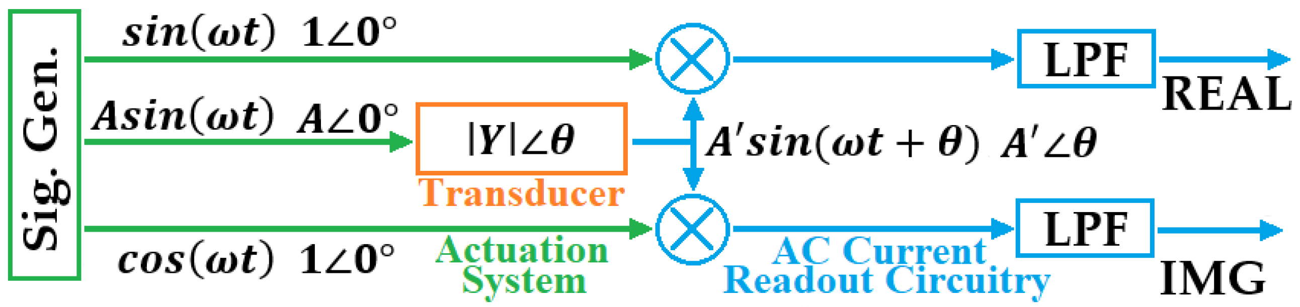
14]), the characterization of a sample by its impedance changes over frequency requires a small stimulus signal, reducing the risk of sample damaging, which is a key point in biological measurement and characterization applications. Information can be then recovered using different readout techniques, being the Fast Fourier Transform (FFT) and the Frequency Response Analyzer (FRA) the two most commonly used. The latter one is based on synchronous demodulation, that is, it relies on phase sensitive detection (PSD) or quadrature modulators to extract the real and imaginary response of the sensor at each input signal
while noise signals at other frequencies are rejected (
Figure 1), presenting advantages compared to FFT algorithms in terms of complexity and speed [
15,
16]. Thus, the FRA-EIS is a more suitable choice to accomplish an autonomous low-cost real-time multichannel impedance spectroscopy analyzer.
In this attempt, while electrochemical transducers take advantage of Complementary Metal-Oxide-Semiconductor (CMOS) processes to implement the required Micro-Electro-Mechanical Systems (MEMS [
17]), the rest of components that conform the data acquisition chain (signal stimuli generators, conditioning, pre-processing and digitization electronics) are still bulky benchtop instruments, making EIS almost exclusively a measurement technique for biochemical, biological, or quality control laboratories, but hindering its use closer to the sampling sources, as milk farms, in food production chains or portable laboratories for on-site tests.
Recent publications in the scientific and technical literature are reporting EIS systems partially implemented using CMOS technologies by addressing specific low-power low-size design techniques to take advantage of the features that miniaturization can provide to the system in terms of portability and high parallelism in the measurement processes [
18,
19,
20]. These cases succeed in the integration of competitive read-out channels, but the generated real/imaginary analog data must be finally digitized to be processed by a digital processing unit (a microcontroller, a digital signal processor or an external computer), while the generation of the required excitation and control signals are usually assigned either to external resources (commercial waveform generators that provide flexibility in exchange of large size and high power consumption, not being compatible with portability), or small size custom integrated oscillators [
21], with exhibit frequency tuning and linearity limitations, especially at high frequencies. Hence, although being fundamental components, both the generation and digitization blocks are not usually considered in the power consumption estimation of the EIS system, thus giving partial information of the real energy required by a complete measurement unit.
In order to reduce electronics complexity, alternative EIS approaches are based on the direct transform of impedance to digital values using impedance-to-digital or dual-slope multiplying ADC (DS-MADC) techniques, achieving accuracies below 10 bits [
22,
23]. With the goal of further reduce electronics complexity, in order to attain a self-contained low-cost measurement system that renders a true portability while preserving high recovery performance, this paper proposes the complete digitalization of the EIS system through a microcontroller-based FRA implementation, applied to impedance spectroscopy for frequencies in the range of cellular characterization, from 1.1 mHz to 10 kHz. The proposed system uses the internal resources of a Propeller processor core from Parallax [
24], to both generate the excitation and control signals required in the process, and to map the read-out and recovery algorithms for the sensed analog signals, so that with minimum additional passive components, it can recover an impedance value with 12-bit accuracy. In addition, the use of this low-cost multicore processor allows for parallelization of the actuation and signal recovery, implementing a multi-channel compact IS instrument on a single microcontroller, able to perform up to 7 real-time in-situ parallel impedance measurements if driven by the same signal generator, or up 4 completely independent parallel impedance measurements; these values can be further extended by accordingly extending the number of cores to allow further parallelization.
This paper is structured as follows:
Section 2 describes the proposed FRA-based impedance analyzer, detailing the implementation and the experimental characterization of both the actuation and the signal acquisition blocks.
Section 3 validates the recovery performance of the proposed IES system applied to an impedance modeling a bilayer lipid membrane. Finally,
Section 4 discusses the proposed approach.
2. Proposed EIS System
The proposed EIS system relies on the use of a single Parallax Propeller microcontroller, characterized by working at up to 80 MHz clock frequency. It presents 8 independent cores plus an additional hub, in charge of controlling the access of each core to the common microcontroller resources (32 kB Main RAM or 32 kB Main ROM), applying a Round Robin schedule. Each core features a video generator, a local 2 kB RAM, and two Counter Modules with Phase-Locked Loops (PLLs) and 32 operation modes (
Figure 2). From a software point of view, the microcontroller can be programmed in C, in its own high-level programming language SPIN, or in low-level Propeller Assembly Language (PASM). In order to achieve a suitable implementation of a FRA-based EIS system, optimizing the hardware resources and their access at the rate needed to generate and recover signals of a reasonable frequency, an integral programming in PASM has been adopted.
2.1. Signal Generation: Hardware Implementation and Control
Figure 3 shows the block diagram of the signal generator hardware implementation. It is based on the D modulation technique to achieve an accurate full range (0 V to 3.3 V) quadrature signal generation needing the minimum number of external passive elements. The first quarter cycle of the two signals to be generated (sine and cosine, from 0 degree to 89.98 degrees) is stored in the shared main RAM memory of the processor. Signal points are stored using a 16-bit representation, with a maximum resolution of 4096 points per quarter. Because the main RAM memory in the processor is composed of 32-bits length registers, each memory position stores the corresponding sine (16 most significant bits—MSB of the memory position) and cosine (16 less significant bits—LSB) values, saving with this choice access time to the global memory and therefore speeding the quadrature signal generation task.
Each core sequentially accesses these data in the main memory at the microcontroller HUB by a Round Robin process schedule, which respectively feeds its two independent hardware Counter Modules, consisting of configurable state machines [
25] working up to the maximum 80 MHz clock frequency. Each counter has an adder and an accumulator, which will be employed to implement the D modulator based on pulse density modulation (PDM) using the carry bit of the adder as modulated output. By properly configuring the operation of both counters in the core, the two sinusoidal signals with 90° phase shift required for an EIS channel can be generated with a single core. An external passive integrator converts the resultant modulated pulses into a sinusoidal signal.
More in detail (
Figure 3), the PDM sine signal generation is performed by a core in the following manner: First, the 32-bit values representing the value of the two quadrature signals at each moment are read consecutively from the main RAM and transferred to the local memory in the selected kernel. Then, the 16 MSB bits (representing the sine value) are extracted and stored in the access register, which is in the adder, and then are added to the accumulator. When the adder overflows, the carry bit changes to 1. The density of 1’s in this output depends on the values that are being added: the higher the values accumulated, the faster the carry overflows. Thus, the density increases in the range of the maximum values of the sine function, while it decreases in the minimum values. Finally, the resulting modulated pulse train is converted into an analog signal by means of a passive second order low-pass filter (LPF) (
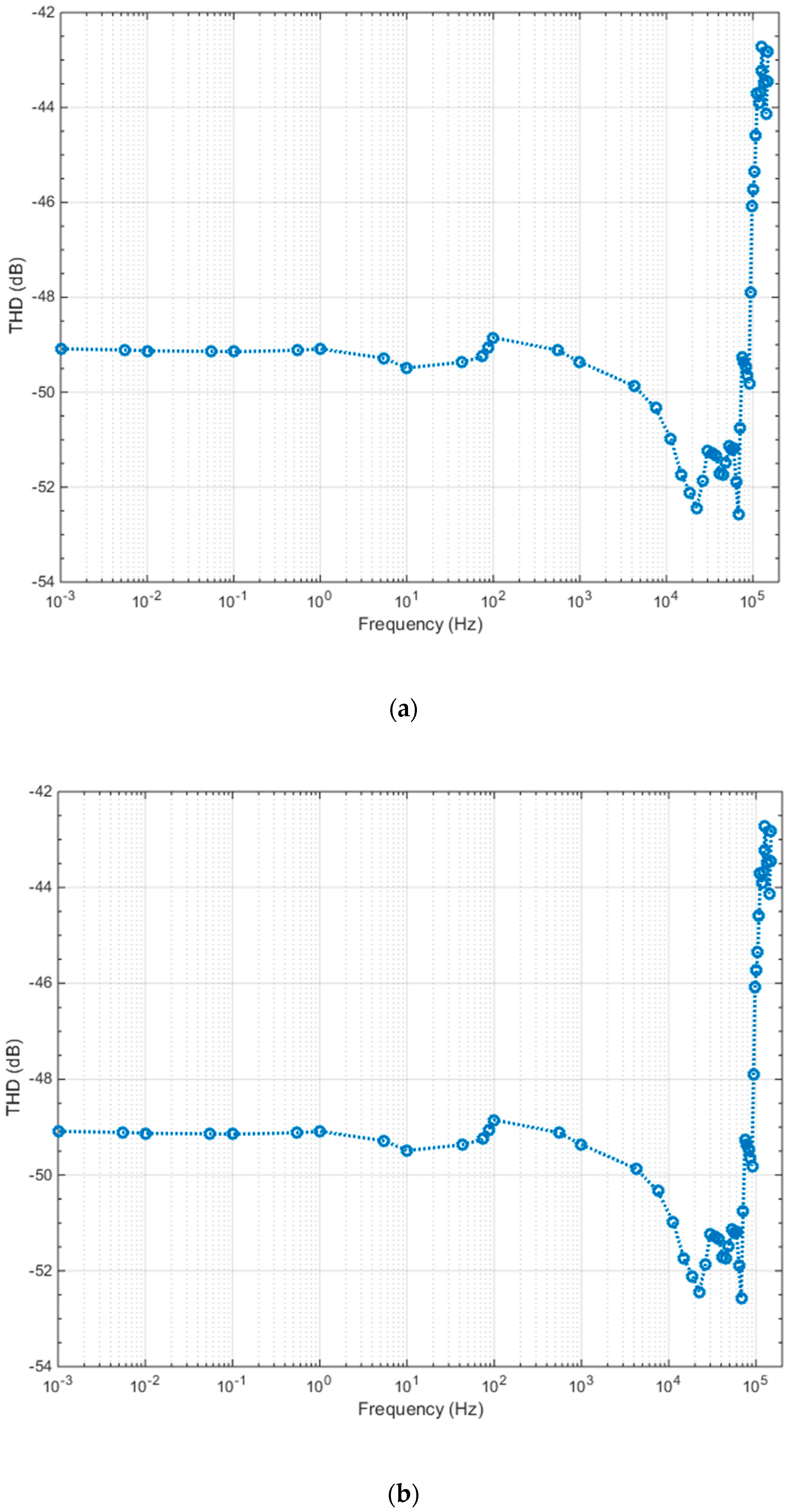
Figure 3) consisting of two cascaded RC circuits (R = 2.2 kW, C = 330 pF) with the same constant time and a factor of 10 in the consecutive R’s and C’s values to reduce the loading effect. The integration time is selected to keep distortion bounded below 0.75% as design specification, as will be shown next.
This process is iterated until all the values in the table are traversed. Next, the process is repeated using the LSB values. These data represent the cosine values in the first quarter of the cycle and, therefore, the sine values in the second, giving therefore signal continuity. To conclude a complete sinusoidal cycle, this process is repeated but changing the sign of the data in RAM to represent the negative half cycle. The cosine generation is performed in a similar manner.
The frequency of the sine/cosine output signal is determined by two different working frequencies: (i) The frequency of the modulated signal, which corresponds to the frequency of the square signal whose density varies. In this work, this signal matches the microcontroller clock frequency, which is set to its maximum value, 80 MHz; (ii) The data generation sampling frequency, that is, the frequency at which the system picks a sine/cosine value from the Main RAM to be sent to the Adder to provide a new output signal value. This frequency, in turn, mainly depends on the microcontroller clock frequency and the number of clock cycles required to load a value into the Adder register from the RAM, being thus more restrictive. An additional control of the output signal frequency can be achieved by selecting not all the samples, but one of every n values at the RAM memory, thus reducing the number of signal points for the generation and therefore reducing the time to generate a signal period.
Taking into account all the aforementioned, the frequency of the sine/cosine output signals
can be expressed as
being the maximum number of samples per signal period equal to
(
samples/quarter × 4),
A is the number of samples not read between two consecutive readings from the memory,
S is the number of clock cycles required to load a sample to the Adder register, and
D is an additional delay that can be added in each reading memory cycle and that serves to achieve a fine tuning in the value of the output signal frequency.
2.2. Signal Generation: Experimental Characterization
By using the degrees of freedom shown in Equation (1), with , S = 65, Arranging from 1 to 2000 and D ranging from 0 to , the frequency can be adjusted to range from 1.1 mHz to 150 kHz in 75 Hz coarse steps (given by parameter ), and fine steps given by D.
Figure 4 shows the PDM signal (carry bit adder pin) provided by the system, when configured to generate
fout = 5 kHz and
fout = 150 kHz sinusoidal output, measured by using a Tektronix
® DPO4104 oscilloscope.
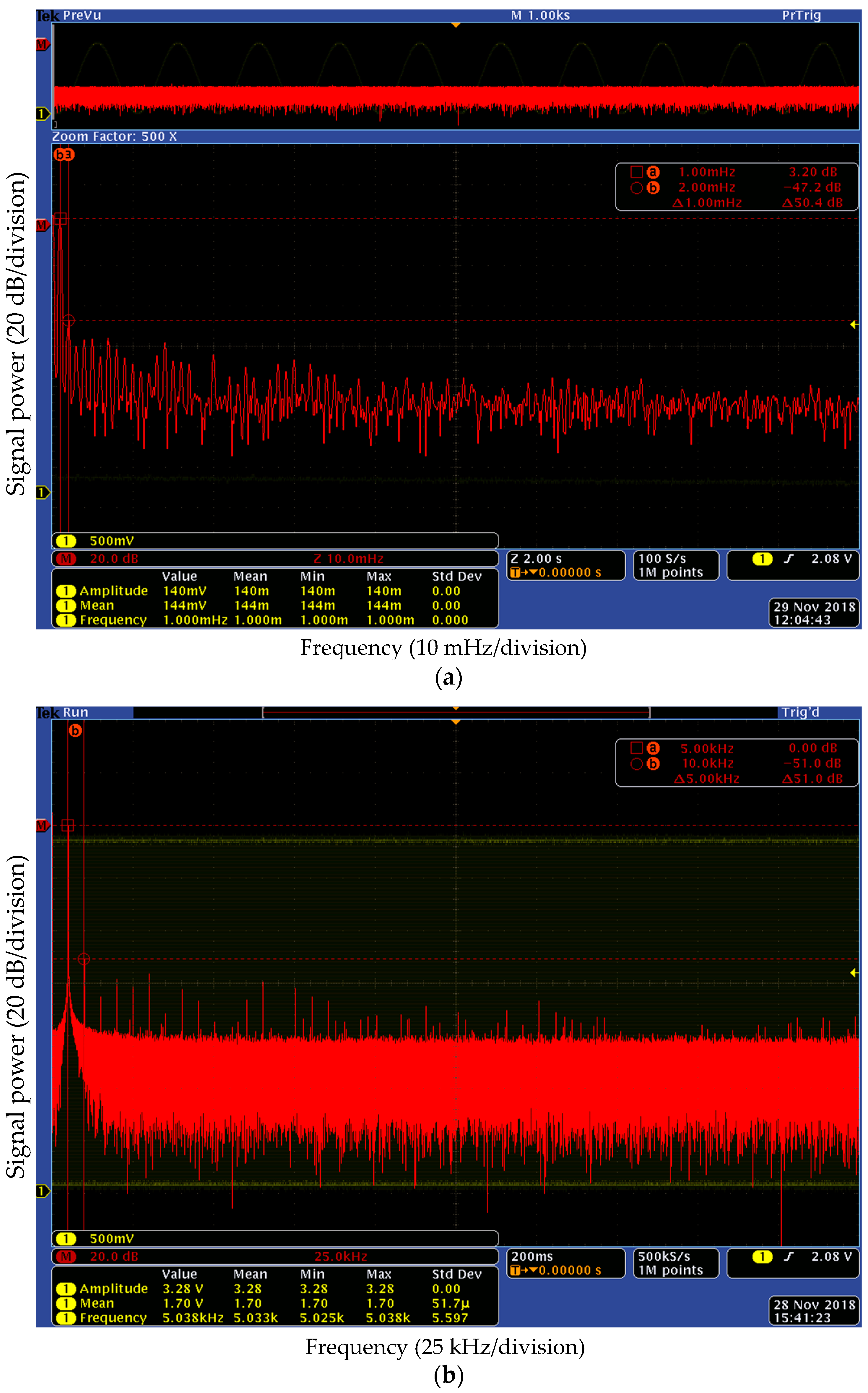
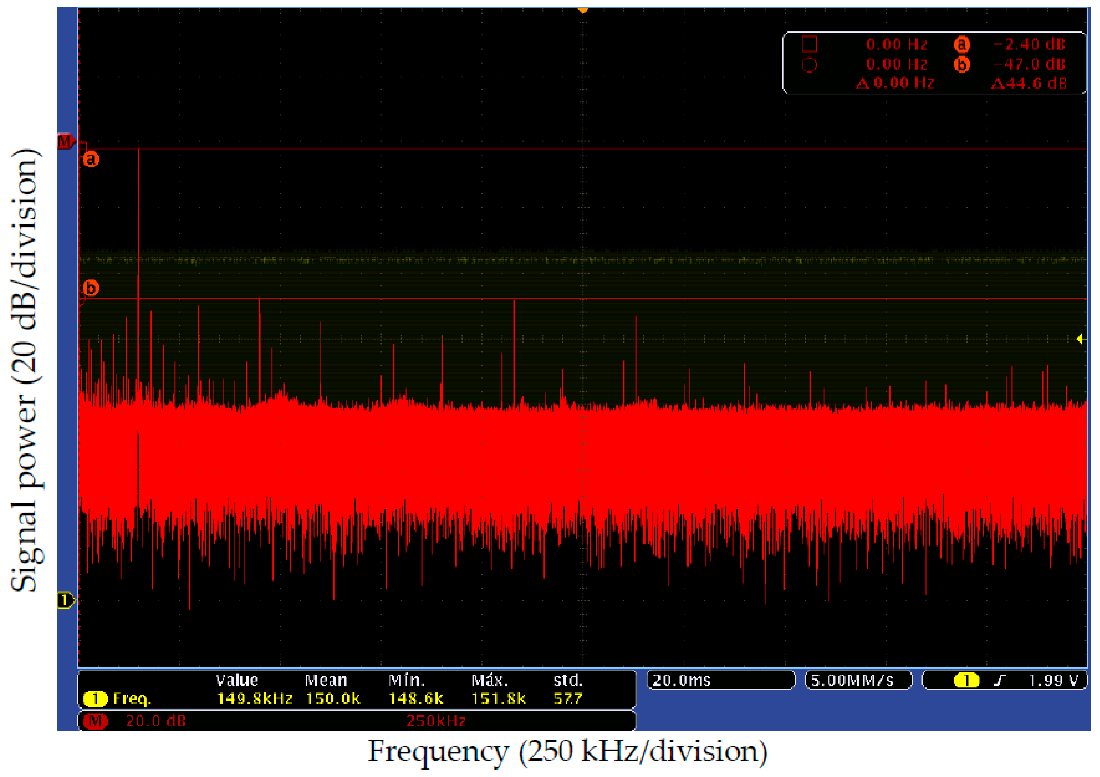
Figure 5 shows the frequency spectrum for the 150 kHz PDM signal (S = 65,
D = 0). The detail box shows the performance closer to the signal of interest, being the 1.080 MHz peak, corresponding to the
frequency, (
fsampling = fclk/(S+D) = 1.23 MHz, Equation (1)), the most relevant interference source. For signals generated at frequencies below 150 kHz, this
interference peak is kept far away enough to be irrelevant. Therefore, by properly selecting the cutoff frequency of the output LPF (
Figure 3), the following sinusoidal signal is set to comply with a maximum distortion (THD and SFDR) below 0.75% over all the frequency range (
Figure 6).
Figure 7 shows the generated sine signals within the operating frequency range, for 1 mHz (
Figure 7a) and 5 kHz (
Figure 7b).
Figure 8 shows their corresponding spectra.
Figure 9 shows the two quadrature signals (sine—yellow and cosine—magenta) after the LPF for the upper and lower limit frequencies of the proposed generator (150 kHz,
Figure 9a and 100 mHz,
Figure 9b). Note that since the counters provide both the carry signal and its negated value, a single core will give two pairs of quadrature signals, that can be used to characterize in parallel two different impedance systems, at the same frequency (signals blue and green in
Figure 9a).
Figure 10 shows the frequency spectrum for the 150 kHz sine; in this case
,
, constituting the worst case distortion.
2.3. Signal Acquisition: Hardware Implementation and Control
The purpose of the signal acquisition stage is to recover the sensor signal to next perform the synchronous mixer operation rendering the corresponding quadrature outputs. The average of these values corresponds to the real and imaginary components or, equivalently, the magnitude and phase of the impedance under test. Note that since the average value of a signal is independent of its frequency, in all this process the signal sampling rate can be relaxed without loss of information. That is why a sigma–delta analog to digital conversion (ΣΔ-ADC) algorithm has been selected in spite of its low conversion rate to accomplish a more accurate conversion. In addition, the ΣΔ-ADC main building blocks can be implemented using the internal resources of a single core, requiring minimum additional external components.
2.3.1. Digitization
Figure 9 shows the block diagram of the ΣΔ-ADC. It consists on a ΣΔ modulator (composed by the integrator, the quantizer and 1-bit Digital-to-Analog Converter DAC blocks) plus a counter module working as a digital decimation filter [
26]. Both the quantizer and the decimation filter have been implemented using the registers of the two counters available in a core. The qualitative operation of this system is as follows [
27]: the analog input (
Figure 11, sensor output signal), through an RC circuit formed by resistor
and capacitor C, provides a voltage value which drives the input of a D flip-flop. While the voltage level in the capacitor is higher than the bi-stable threshold (assuming the threshold voltage in the bi-stable is half the digital bias voltage,
VDD/2), its output
remains
(and
). This Output
enables the accumulator operation, increasing the value in this register for each new clock cycle. On the other hand, the output
conforms a negative feedback loop to the input capacitor through resistor
that reduces the voltage at the integrating capacitor. Once the voltage at input D gets under the threshold value, outputs
and
flip their values at the next clock cycle. The accumulator stops increasing its value, providing a binary value related to the number of cycles that the voltage value at the analog input remains greater than the threshold value. The resolution in which the analog value is represented by the Serial Digital Out depends on the selected integration time.
In fact, the application of the circuit shown in
Figure 11 to time-dependent signals presents some constrains related to the cutoff frequency of the input low-pass filter, the frequency of the input signal and the conversion frequency to guarantee a suitable estimation of the input sample. For the sake of simplicity, let us suppose the sigma-delta modulator works in linear mode (that is, the clock frequency is much higher than input signal frequency, therefore considering its operation mode as continuous). Then, the block diagram of the ΣΔ modulator in the S domain is given by the scheme in
Figure 12 [
26].
Where
is the input voltage and
is the output
in
Figure 11, while
N(s) represents the effect of quantization in the transfer function, which is negligible if linear operation is assumed. The ΣΔ modulator transfer function is
and accordingly, the output voltage can be expressed as
where K is proportional to the D flip-flop threshold voltage,
VDD/2. Therefore, the output voltage depends on the
passive filter cutoff frequency and the input signal frequency
. Thus, an input signal with a frequency higher than
may result in a loss of accuracy. Besides, the conversion frequency
must be fast enough to avoid that the capacitor discharge process affects the digitized value, which would reduce the resolution in bits of the ADC. That is, on the overall it must be satisfied
being necessary to appropriately select the passive components in the modulator stage as well as the conversion rate in order to perform a suitable signal digitization in N bits.
To manage the hardware resources to reliably perform the required operations while minimizing the execution time, a specific code using the microcontroller assembler has been developed.
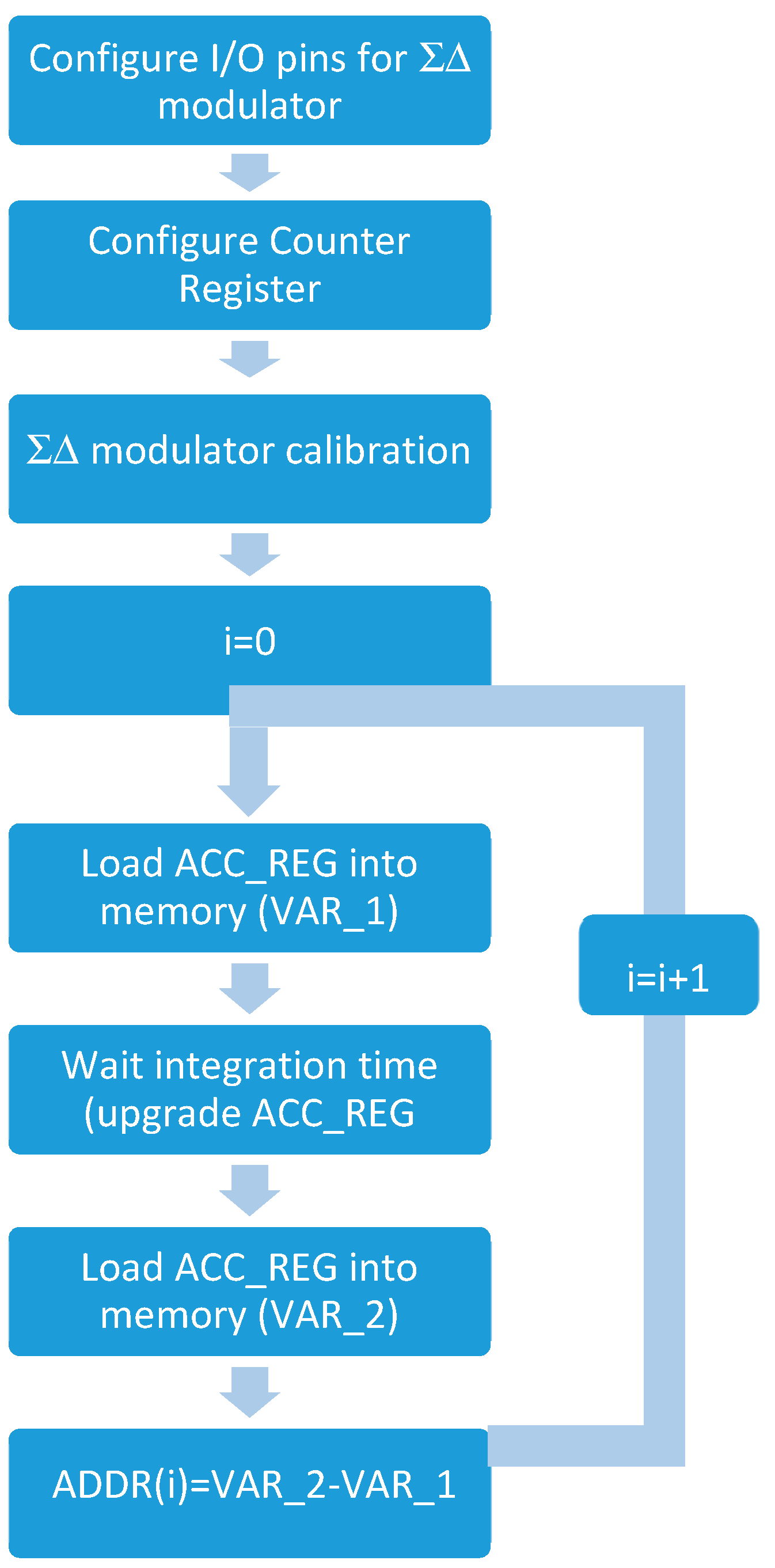
Figure 13 shows the simplified control flowchart describing the signal digitization and data acquisition. After configuring the corresponding input and output pins and the counter register, first a calibration process is carried out. This task, which is performed at the system start up, allows determine both the offset at 0 V in the accumulator and the integration time required to properly acquire the maximum allowable input voltage, therefore maximizing the dynamic range. For completing the calibration step, the Analog Input (
Figure 11) is connected to 0 V. After the integration time, the value stored in the accumulator, which ideally should be equal to zero, is the excess offset reading that must be subtracted from the system readings in normal operation mode. The integration time is adjusted by applying the maximum voltage to be digitized in the Analog Input. After the integration time, the accumulator should be filled to the maximum value (
), keeping the overflow flag equal to zero. Otherwise, the integration time must be increased/decreased up to reach this condition for a given number N of bits.
Once calibrated, the system temporally saves the value stored in the counter accumulator in a variable, waits the integration time and reads again the value in the register. The difference between both data represents the value of the sensor output signal at this time, which is stored in a memory address so that data from consecutive instants of time use consecutive memory positions.
2.3.2. Mixing and Averaging
In a Propeller microcontroller, the hardware resources allow digitizing up to two different signals in parallel per core. To accurately synchronize the mixers operation, the system makes use of a dedicated core for each impedance measurement according to the following process: one of the counters is dedicated to digitize the signal arriving from the impedance under study, while the other counter synchronously digitizes the original sinusoidal excitation signal. The product of these two data corresponds to the real mixer output. The real component of the impedance under test is then calculated by averaging the products provided by this branch over a minimum n = 5 periods of the excitation signal to obtain reliable results over all the operating frequency range. In a single-channel measurement approach, the quadrature signal, which does not excite the impedance under study (cosine) is directly read from the hub memory, feeding the corresponding mixer (Imaginary) before its averaging, thus making unnecessary its digitization, which saves both hardware as computing resources.
2.4. Signal Acquisition: Experimental Characterization
The structure shown in
Figure 11 has been implemented for a 12-bit approach. First, the linearity of the analog-to-digital conversion is verified by applying an incremental DC voltage in the biasing range of the microcontroller (from 0 to 3.3 V) to the Analog Input of the ΣΔ-ADC (
Figure 11), and recovering the output digital values.
Figure 14 shows the results, where y axis corresponds to the analog values represented by the digital words obtained in the conversion, assuming a full scale digitization (that is, 000h represents 0 V and FFFh represents 3.3 V in hexadecimal). It can be seen in this figure that the ADC conversion presents high linearity, resulting in a gain or slope of 0.65, an offset below 18 mV, and with a coefficient of determination
. The conversion slope can be modified by the feedback loop through
(Equation (3)), to adjust its value according to the conversion requirements. In this case, to allow a full sweep in the supply voltage range avoiding saturation in the digitization module (
Figure 11), we kept the output gain < 1 by selecting
and
. This choice results in a conservative 0.65 gain, exactly as obtained from the linear fit.
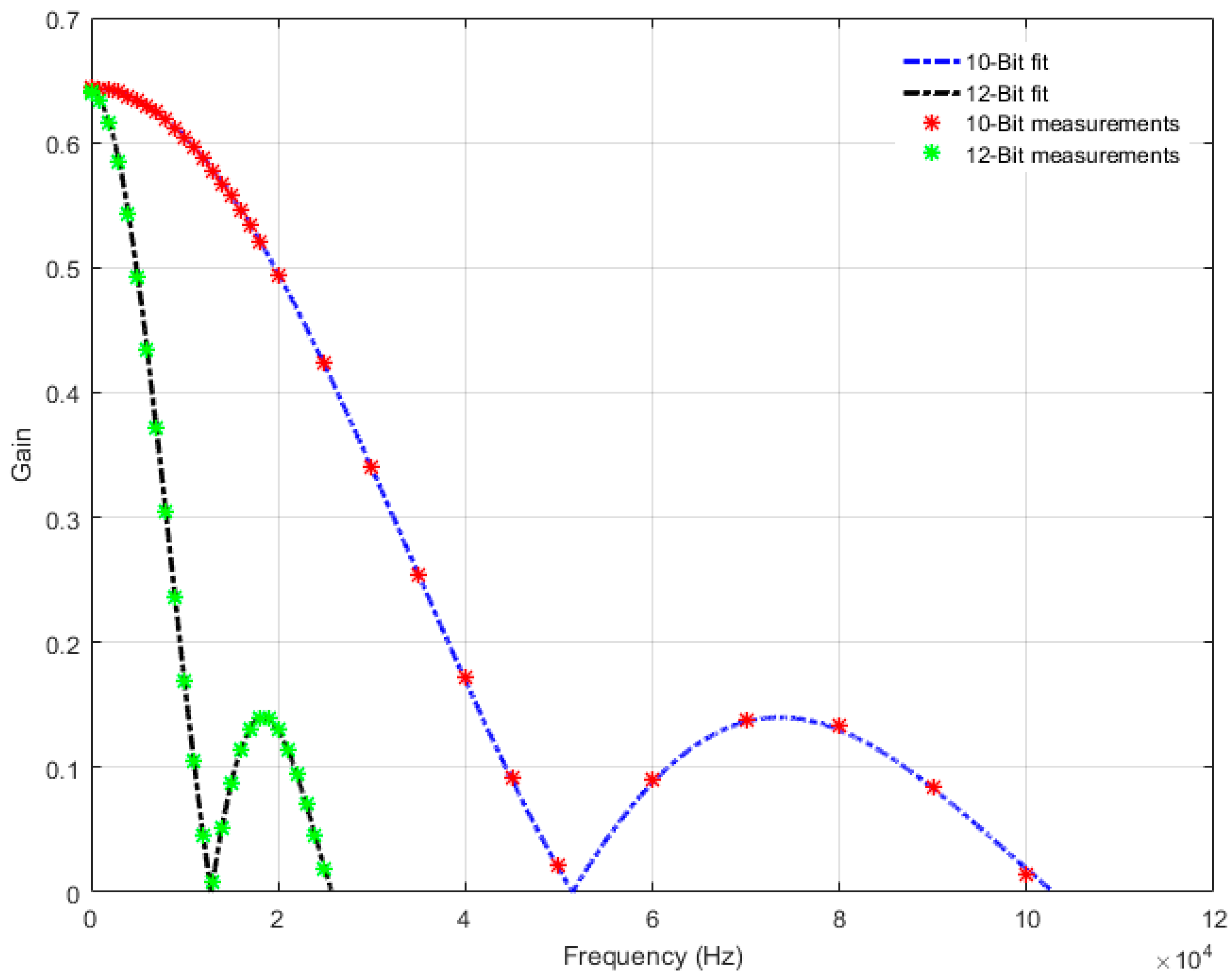
Figure 15 shows the gain versus frequency characteristic of the proposed ADC configuration, for 10-bit (red dots) and 12-bit (green dots) output resolution, which presents the typical
sinc digital filter shape, matching with the previous DC characterization. According to this figure, a 12-bit ADC is selected, to enhance resolution and preserving the frequency of operation up to the 10 kHz range.
Finally,
Figure 16 presents the voltage values acquired using the ADC (red dots) from a 5 kHz sine signal, and the corresponding cosine values (recovered from the RAM memory using the instant sine values acquired). Both show a good matching when represented over their corresponding original full signals. These values are the inputs for the mixing operation.
3. Results
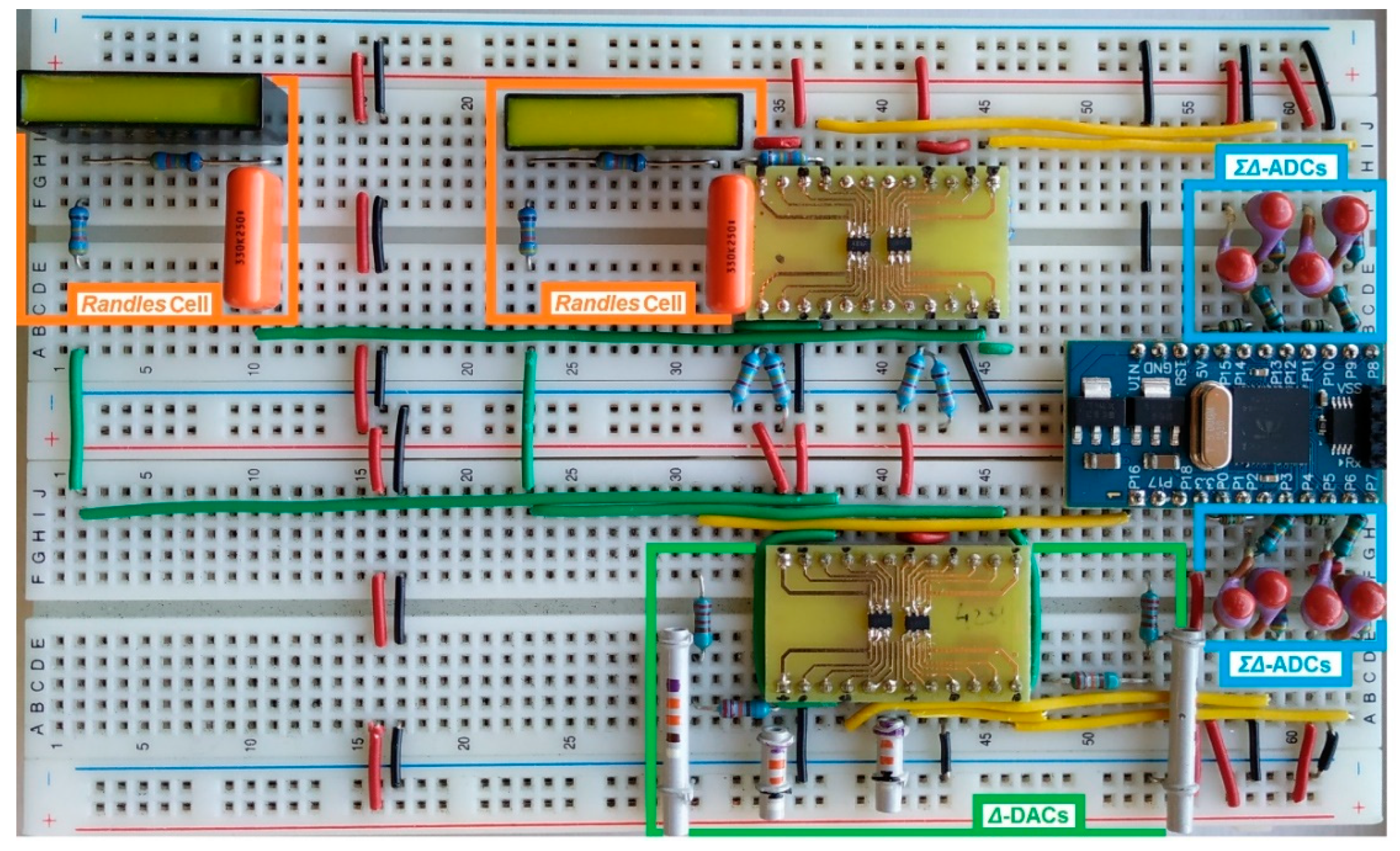
The EIS system schematic, considering a two-channel measurement approach, is shown in
Figure 17, and the prototype photograph is shown in
Figure 18. In
Figure 17, Block (a) corresponds to the signal generation module, including the digital Counter Module in the corresponding core and the R-C low-pass filter (
). It is followed by an impedance adapter element (a simple voltage follower), which allows transferring the generated signal to the cell under test. For real biological applications, this module can be replaced by voltage or current reduction modules suited for the target application. The Randles cell representing the impedance sample corresponds to Block (b). Note that each Randles cell is followed by a transimpedance amplifier (TIA) consisting on an Operational Amplifier with a feedback resistor
Rf2, that converts the current
IZ provided by the biocell into a voltage value
VZ = −
Rf2IZ for its digitization. Block (c) represents the implemented ΣΔ-ADC -based system that conforms the synchronously digitized impedance extraction; the passive components values are (
), where
RC + RSD corresponds to
R1 in
Figure 11. This configuration allows calibrate the operation of the ADC (
Figure 17) by setting the voltage value in (A) at the required values through the ΣΔ calibration pin without the need of deactivating the operation of the cell, thus with minimum waste of time.
Application to Impedance Spectroscopy
The system operation as a frequency response analyzer applied to impedance spectroscopy has been tested using the characteristic impedance of a biological model based on the bilayer lipid membrane presented in [
28,
29] (
Figure 19). The associated Randles cell is modeled using three impedances whose values are:
Rm = 434 kW,
Cm = 580 nF and
Cdl = 340 nF (
Figure 17). The resistor
Rs represents the impedance associated to the sensing electrodes, which can vary from negligible values up to a few MW. In this work, an intermediate value of 500 kW has been selected. The TIA active block in
Figure 17, Block (c) is a MAX4231, and resistor
Rf2 = 500 kW to accommodate a full analog voltage input range of 0 to
.
For a normalized amplitude excitation signal with operating frequency
fin, the corresponding output biosensor signal
is given by
where
Z represents the cell impedance.
The digitized values of the biosensor signal are multiplied in the corresponding microcontroller core by the respective digital sine and cosine values, and the results are averaged over an integer number
n of signal periods (with
n minimum = 5 as pointed in
Section 2.3.2), so that:
Note that since each digitization at the ΣΔ-ADC requires a minimum of 2
12 clock cycles (for a 12-bit resolution), the two mixing and accumulation cycles are performed in real time by computational resources in the same core. Thus, impedance magnitude and phase shift can be recovered as
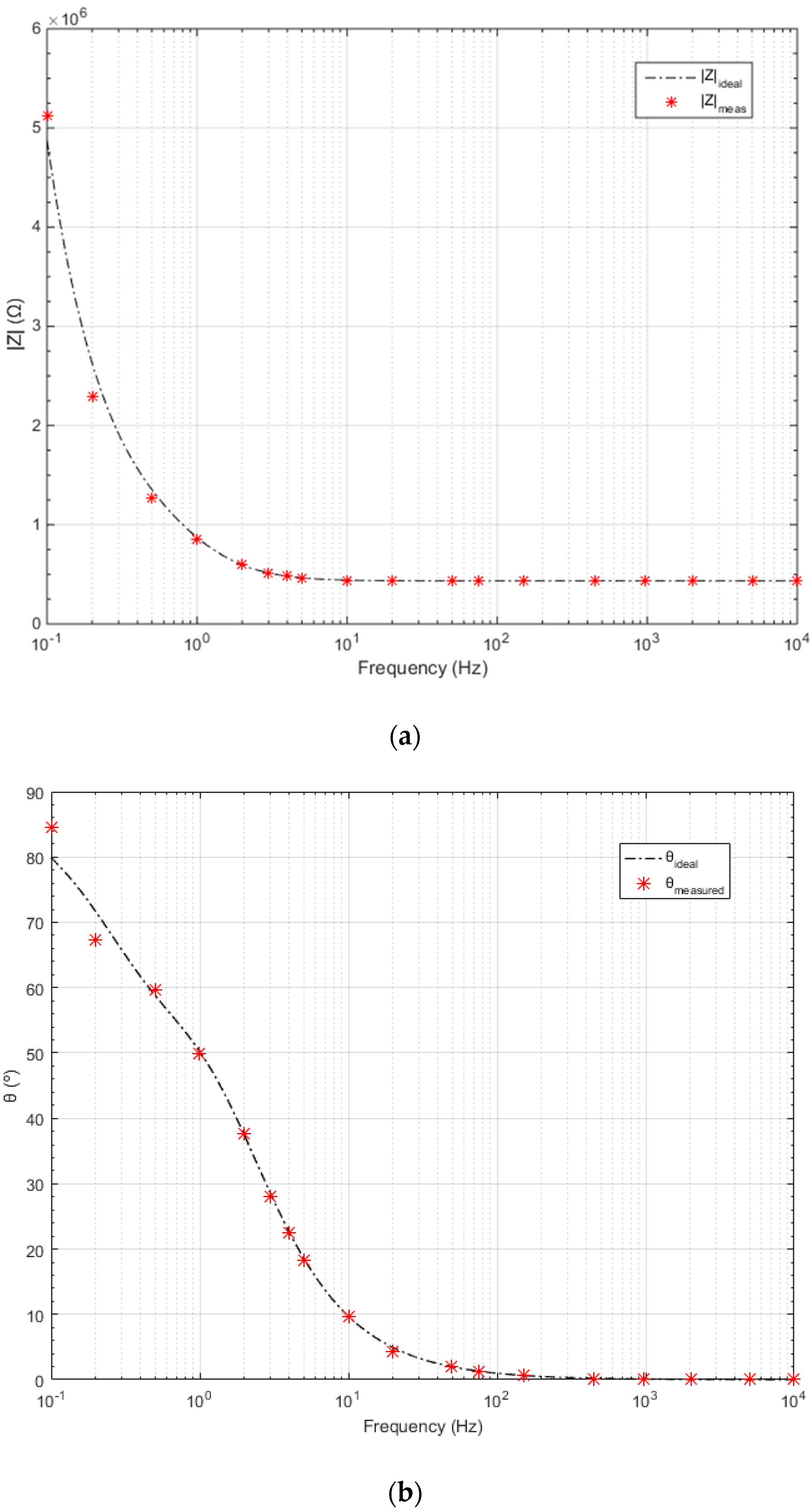
The impedance characterization has been performed for 18 frequency values in the 100 mHz to 10 kHz range at 12-bit resolution. Since for each of these measurements an acquisition time of at least 5 signal cycles has been guaranteed, a total time of 100 s is required for the complete characterization over frequency.
Figure 20a shows the impedance magnitude recovery performance compared to the ideal values, while
Figure 20b presents the phase evolution.
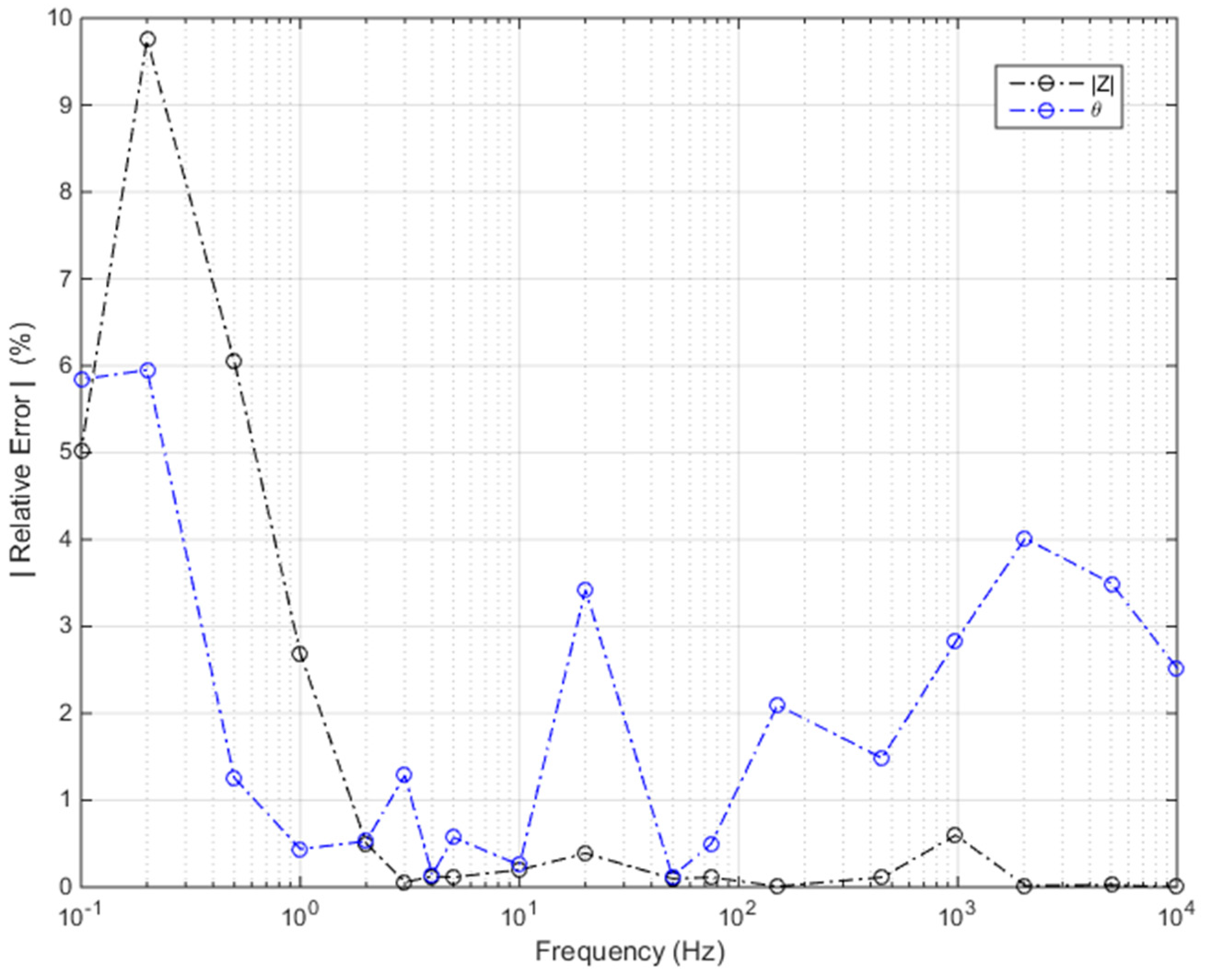
Figure 21 shows the impedance magnitude and phase relative error achieved estimating both values.
4. Discussion
This paper has presented a compact multi-channel FRA-IS instrument that fully relies on a low cost Propeller multicore microcontroller, accomplishing a complete actuation-detection solution needing minimum additional external components. The excitation signal for impedance characterization is generated by a PDM-based generator running on a single core. This module generates up to two pairs of quadrature signals at a single frequency, so that the number of cells to be characterized at the same time can be highly extended by using adaptation modules (voltage followers in
Figure 14) connected to the different signal generation ports. In this way, the (bio)impedance characterization processes can be highly parallelized, as it is demanded by current array-based applications. Signal recovery for impedance characterization is performed using the rest of available cores in the microcontroller, being possible to simultaneously acquire up to 7 impedance measurements, one per core. This number can be proportionally widened by extending the number of microcontrollers where the ΣΔ algorithm is implemented in the reading process, provided they receive the excitation and sensor output signals.
On the other hand, the proposed architecture allows impedance characterization using different excitation frequencies for several Randles cells in parallel, just assigning a different generation core per frequency. In fact, a more general solution could consist on assigning the cores of a Propeller microcontroller to generate the different frequencies (implementing the corresponding PDM and LPF per core), while using additional Propeller microcontrollers dedicated to the acquisition and impedance measurement tasks, implementing the ΣΔ-ADC in each of the processor cores.
Therefore, the proposed EIS system constitutes a fully operative flexible and modular solution, suitable for multi-channel acquisition while complying the features of portability, and with an enhanced trade-off between low cost and measurement performance compared to similar devices in the literature. Reviewing the state-of-art, a direct approach relies on the use of the component AD5933 or the newer ADuCM350, which shown satisfactory results in different applications [
4,
11], but performing one measurement process at a time, and at the cost of the high computing power required to implement the Discrete Fourier Transform (DFT) compared to the FRA technique. Similarly, comparable alternative low-cost microcontroller-based EIS architectures [
30,
31] need more complex external hardware, providing typically worst resolution while covering a similar frequency range and for a single channel impedance measurement. Finally,
Table 1 compares the implemented analyzer performances with those of previous multichannel implementations operating at a similar frequency range. It can be seen that our proposal achieves better resolution over a wider frequency range.
Therefore, the proposed approach succeeds in reducing instrument dimensions to allow automatic and in-situ multichannel impedance measurements, while improving the measurement performance using low-cost commercial components off the shelf (COTS).


