Integration of Optical and Thermal Models for Organic Light-Emitting Diodes

1
Graduate Institute of Energy Engineering, National Central University, Taoyuan 320, Taiwan
2
Department of Mechanical Engineering, National Central University, Taoyuan 320, Taiwan
3
Instrument Technology Research Center, National Applied Research Laboratories, Hsinchu 300, Taiwan
*
Author to whom correspondence should be addressed.
Electronics 2019, 8(1), 17; https://doi.org/10.3390/electronics8010017
Submission received: 29 November 2018
/
Revised: 14 December 2018
/
Accepted: 19 December 2018
/
Published: 23 December 2018
(This article belongs to the Special Issue Organic Light Emitting Diodes - OLEDs)
Abstract
:This paper proposes a three-dimensional model for combinative analysis of the illuminative and thermal properties of organic light-emitting diodes (OLED). By means of the energy conversion ratio and energy conservation theory, two individual optical and thermal sub-models are integrated to form a single model constructed in a multi-physics platform. According to the measured luminous performance and temperature distribution of the fabricated OLED samples, the proposed model demonstrates sufficient accuracy. Moreover, the temperature distribution on the cross-section of the OLED can be derived from the proposed model and used as a valuable reference for manufacturers to select appropriate organic materials.
1. Introduction
With the development of solid-state lighting technology, light-emitting diodes (LED) have been applied to many different types of lighting products and have gradually dominated the common lighting market. Meanwhile organic light-emitting diodes (OLED) have shown high potential to replace surface lighting sources, such as indoor and decorative luminaires [1]. Although OLEDs are thin, flat, flexible, and provide a comfortable light source with a large-emitting area, challenges involving increasing panel sizes, improving luminous efficiency, and reducing manufacturing costs remain before OLEDs may be introduced to the lighting market [2]. Advanced OLED display technology has the advantages of high contrast and low energy consumption, while at the same time demonstrating a fast response time and a large viewing angle [1]. When used in lighting applications, on the other hand, OLEDs should exhibit uniform emissions, sufficient luminous flux, and appropriate luminous intensity distribution. Since OLED luminaires are generally regarded as large-area lighting devices, the ability of these light sources to exhibit uniform emissions is of great importance. The luminance uniformity of these sources is closely related to spatial temperature distribution [2,3,4,5,6], so greater attention has been focused on the thermal aspects of OLEDs [7]. Therefore, in addition to the conventional optical performance, the thermal characteristics of OLEDs will also be investigated in this study. Several studies have constructed models for investigating the optical and thermal properties of OLEDs, with some also accounting for their electrical properties. Such models employ fluid dynamics, successive network reductions, equivalent circuits, spectral power distributions, and so on [2,3,4,5,8,9,10,11,12,13].
This study proposes an alternative modelling approach: a three-dimensional (3D) model to be used to simultaneously explore the optical and thermal performances of OLEDs. The proposed 3D OLED model integrates the optical and thermal sub-models by means of the energy conservation theory. According to the comparisons between experiment and the simulation, the proposed 3D model can predict the luminous properties and the thermal distributions of OLEDs with acceptable accuracy. Herein, the limitations of OLED modeling are discussed, and successive modeling demands for future development of OLEDs are projected.
2. Model
The proposed 3D OLED model is constructed using two sub-models, with each accounting for a specific property of the OLEDs. The thermal sub-model predicts the temperature distribution of an OLED device, while the optical sub-model simulates the luminous performance of the device. Using the parameters of the energy-conversion ratios, the two sub-models are then integrated into a single model. To construct such a 3D model, both sub-models are established geometrically in a multiphysics-embedded platform, COMSOL, and a bottom-emission OLED device is used as an example. The geometry of the example device is modeled using the following the layers: an upper cover (glass), followed by a cathode (Al), organics, an anode (indium tin oxide, ITO), and finally a base (glass). To model a practical OLED sample, we consider an available OLED whose base glass with the dimensions of 40 mm × 40 mm × 1 mm, and the dimensions of other layers are listed in Table 1. The details of each sub-model are described in the following sections.
2.1. Thermal Sub-Model
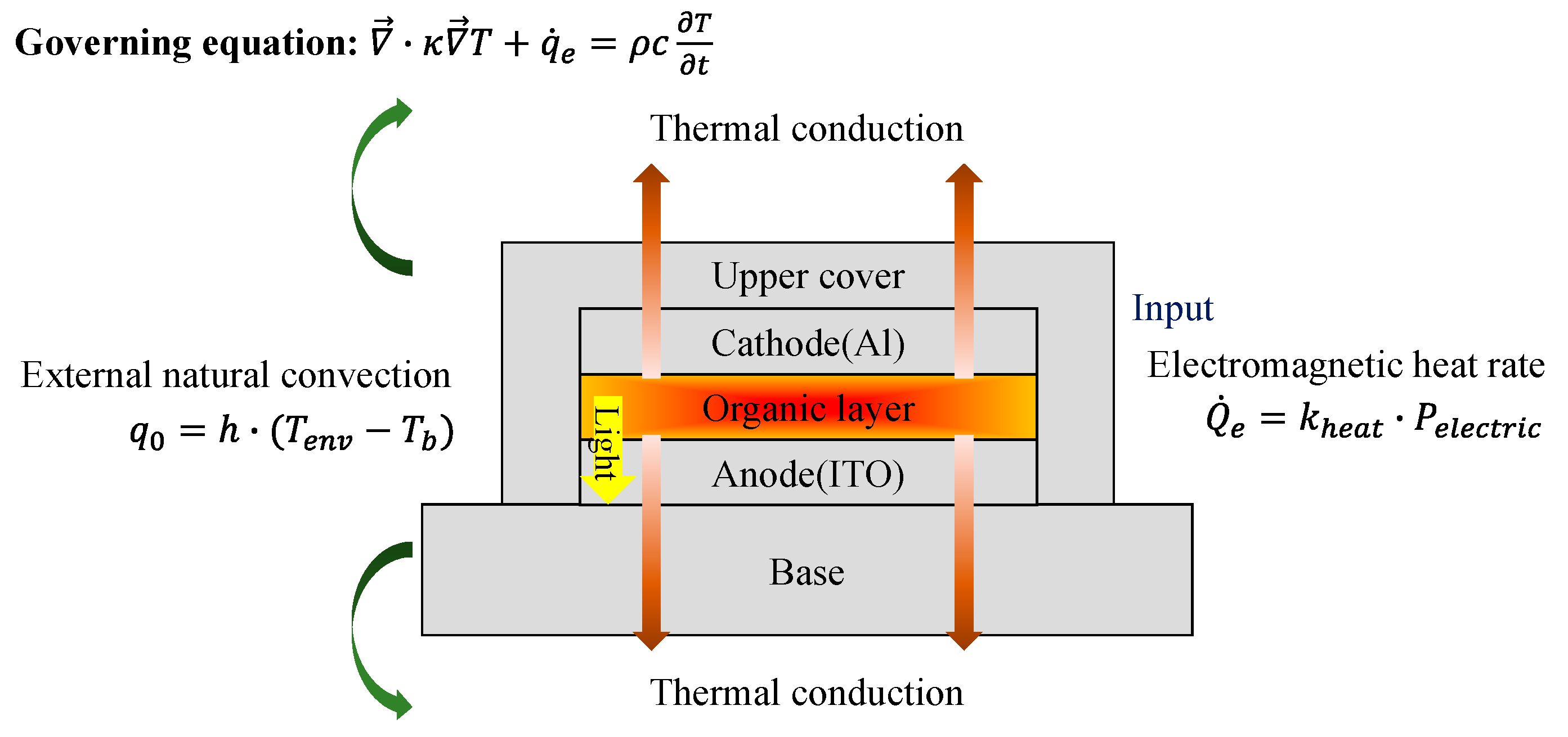
To investigate the thermal effect in OLEDs, the governing mechanisms of heat dissipation, including conduction between layers, conduction at the electrodes, convection between the OLED and the environment, and radiation from the OLED are considered in the thermal sub-model. The types of thermal dissipation for each OLED layer along with their equations are shown in Figure 1.
The governing equation of the boundary conditions is based on the 3D heat equation [17]:
where κi, Ti, ρi, and ci are the thermal conductivity, temperature, density, and specific heat of each considered layer, respectively; is the power of the heat converted from the input electrical power, Pelectric, per unit volume. The volumetric power can be expressed as:
where Vorganic is volume of the organic layer. is the electromagnetic heat rate and can be derived from the input electrical power:
where kheat is the proportion of input electrical power converted to the thermal power. Equation (3) describes the thermal conduction of the considered layer based on the Fourier’s law of conduction. To describe the steady state conditions of the entire thermal system, the device and its surroundings are assumed to experience natural convection, and the equation can be expressed as [5]:
where h, Tenv, and Tb are the heat transfer coefficient, ambient temperature, and boundary temperature of the device, respectively. Along with the material parameters of the example device, as listed in Table 2, and the parameters of governing equations, the thermal characteristics of the device, such as temperature distributions on the surfaces, can be calculated from the proposed thermal sub-model.
2.2. Optical Sub-Model
The optical sub-model of an OLED is constructed to investigate its lighting performance, including the luminous flux, illuminance at a target plane, luminous intensity distribution, etc. Because such performances relate to the far-field characteristics of the device, the propagation of light is modeled approximately using geometrical ray-tracing. Similarly to the thermal sub-model, the lamination of multiple organic materials with sub-micron thicknesses is regarded as one integrated organic layer in the optical sub-model. In order to increase the modeling accuracy, the Fresnel equations are applied for those refractive interfaces, while the diffuse scattering is calculated for the reflective cathode according to Lambert’s cosine law. The refractive index, thickness, and optical property of each layer of the example device are listed in Table 1. In order to quantify the total out-coupling luminous flux, a far-field spherical receiver is built herein. The light-extraction efficiency (ηLEE), defined as the ratio between the out-coupling light power and the power that is emitted from the organic layer, can then be calculated. To analyze the luminous intensity and illuminance distributions, a flat receiver positioned 1 m away from the organic layer is constructed in the form of square mesh. The dimensions of the flat receiver are 5.5 m × 5.5 m, leading to an analyzable range of luminous intensity between 70° and −70°. Once the flat receiver acquires the illuminance data of every mesh, the illuminance of the ith mesh, Ei, can be converted into luminous intensity, Ii. Consider a ray emits from the source toward the ith mesh, as shown in Figure 2. Assume that ri is the distance between the source and the ith small mesh whose area is dAi, and θi is the angle of incidence for the ith mesh. Then the projected area of the ith mesh on to the surface normal to the ray can be counted as dai = dAi · cosθi. According to the radiometry, the luminous flux through the ith mesh is Ei · dAi = Ii · dai / ri2. A conversion formula is then derived as follows:
where Z is the normal distance between the source and the flat receiver.
Notably, the proposed method for building an optical sub-model is adaptive for use with an arbitrary optical simulation tool that is based on geometric ray-tracing. In order to link the thermal sub-model, the optical simulation is performed using the same modeling platform, COMSOL, but a different module; namely, the ray optics module. Since a ray-tracing tool generally regards light propagation as ray trajectories, a greater number of rays result in higher simulation accuracy, but with longer calculation time. The constructed optical sub-model is then pretested to optimize the number of rays required. It is found that when the number of rays is greater than 5 million, the light extraction efficiency calculated from the simulated luminous flux attains a stable value of ηLEE = 27.3%. Because such a pretest considers only the emitted light power and does not account for the thermal effects, this test may also be performed using other optical simulation tools in order to confirm the results derived from COMSOL. LightTools is chosen because of its wide acceptance in the lighting industry. After the optimization of the number of rays, the simulation via LightTools calculates the ηLEE as 26.7%, close to that calculated by COMSOL. Both results are reasonable when compared to experimental data from literatures [21,22].
2.3. Integration of Sub-Models
The proposed optical and thermal sub-models are then integrated based on energy conservation theory. It is assumed that the input electric power, Pelectric, for the OLED device is converted to both optical and thermal power, and that other types of converted energy are negligible. Based on energy conservation theory, the input electric power ideally can be expressed as [9,13]:
where Plight is the power of light generation, and Pheat is the thermal power, which is equivalent to the power of heat: Pheat = Qe. Similarly to kheat, which is the ratio of the power of heat source to the input electrical power, a parameter klight is defined as a ratio of the power for light generation to the input electrical power:
From Equations (2), (6), and (7), the relationship between kheat and klight can be derived as:
According to the light extraction and optical loss mechanisms of OLEDs [14,23,24], the power for light generation results from several phenomena and is expressed as:
where ηEE, γ, ηS/T, and ηrad are the electrical efficiency, the ratio of injected charge carriers that form excitons, the singlet and triplet fractions of excitons, and the ratio of the singlet and the triplet excitons which cause luminescent radiation, respectively. The last term, ηrad, can be comprehended as the synthetic results of the photoluminescence of the acceptor and the transfer of singlet and triplet excitons from donors to acceptors [25]. Equations (7) and (9) show also that klight is the synthetic effect of ηEE, γ, ηS/T, and ηrad. The luminescent light then encounters several optical ray-trapping mechanisms, such as the total internal effects in the substrate and other layers, as well as the surface plasma attenuation, etc. Only the extracted rays contribute to the final out-coupling light power, Poutput:
A parameter of radiant efficiency, ηo/e, is defined herein as the ratio of the output light power and the input electric power. From Equations (6)–(10), ηo/e can be derived as:
Since the product of the central three terms is known as the internal quantum efficiency, IQE = γ · ηS/T · ηrad, and the product of IQE and ηLEE equals the external quantum efficiency, EQE, the radiant efficiency can be also expressed as:
On the other hand, since the input electric power, Pelectric, is assumed to be transformed only of the optical and thermal powers, the full amount of electric power is implied to be received by the OLED device with an electrical efficiency, ηEE, of unity. The internal quantum efficiency, IQE, and klight therefore can be regarded as equivalent:
Using Equations (2), (6)–(8), and (12), the power for light generation, Plight, that for heat, Pheat, and that of the output, Poutput, can be calculated using the proposed sub–models. In order to resolve these equations, the input electric power, Pelectric, equivalent to the product of the input current and voltage, and the parameter klight must be provided. Once Plight and Pheat have been derived, the aforementioned optical and thermal performances can be calculated using the proposed models. In other words, the optical and thermal sub-models can be linked as one synergetic model based on energy conservation theory and the given parameters.
In this study, the optical sub-model is calculated using the ray-optics module of COMSOL and utilizes both a far-field receiver and a large receiver, which correspond to coarse and fine resolutions, respectively. The thermal sub-model is calculated by the finite element method (FEM) via the heat-transfer-in-solid and the electric-current modules of COMSOL with its geometry constructed in the far-field configuration. The two configurations are then further integrated to become one model. The final model consists of the two sub-models, while their individual energy ratios are determined based on energy conservation theory.
3. Experiments and Discussions
3.1. Sample Preparation
Green phosphorescent OLEDs were fabricated by the conventional processes to demonstrate the proposed model experimentally. Firstly, the glass substrate was coated with the ITO, which was then etched to form the patterned anode. Next, the multiple organic layers were evaporated onto the patterned ITO, followed by the evaporation of the Al/LiF cathode. Finally, the glass passivation was allocated above the cathode, and glue was used to seal the sample. Among the organic layers, the essential green emitter was the combination of WPH-401 and WPGD-831 fabricated by Shine Materials Technology Co. Ltd. The dimensions are listed in Table 1, and the emitting area is 1 cm2, as shown in Figure 3. Eight samples were made via the same process with identical parameters for the following investigation.
3.2. Electrical Properties
The current-voltage (I-V) curves of the OLED samples were measured using a semiconductor device analyzer (Keysight B1500A). In laboratorial experiments, even the same run of the process practically produces samples with a certain discrepancy. Thus, the measured results of the eight samples were then averaged and converted to a current density-voltage (J-V) curve by counting the emitting area, as shown in Figure 4. This shows that when the operation voltage is 5 V, the average current and input electrical power are 23 mA and 115 mW, respectively. In this example, these parameters are then used as input values for the proposed model.
The luminous flux of each sample was measured using a 15-cm-diameter integrating sphere (ISUZU IOC-6) equipped with a spectrometer. Under an operation voltage of 5 V, the current, radiant power, Poutput, and radiant efficiency, ηo/e, of each sample were measured and calculated. It is noteworthy that, although the output radiant power was measured in the unit of milliwatt, this data can be converted to the commonly used luminous-flux unit of lumen by means of the photopic spectral luminous efficiency curve. Thus, the out-coupling luminous flux was also obtained, and the averaged result was 5.3 lm, equivalent to 9.74 mW for the samples herein. Although the measured current through each sample differed, the resultant radiant efficiencies were similar. The average radiant efficiency of the samples was then calculated as (ηo/e)ave = 8.45%. By means of the optical sub-model and the aforementioned parameters, the relationship between klight and ηo/e is obtained, and klight is calculated to be 0.31 at the measured radiant efficiency. Once klight is obtained, the internal quantum efficiency, IQE, can be derived from Eq. (13). Next, using Eq. (8), the ratio kheat is calculated to be 0.69. Since klight and kheat are now determined, both sub-models provide absolute rather than relative results.
3.3. Thermal Properties
The thermal properties of the fabricated samples were investigated via temperature measurements. The temperature distribution on the upper cover of the OLED was measured using a thermal imager (InfraTec VarioCAM), while the ambient temperature was set as 24.6 °C with the accuracy of ±0.3 °C As shown in Figure 5, the resultant maximum and minimum temperatures of the samples are in the ranges of 30 °Cߝ32.5 °C and 24.5 °Cߝ25.6 °C, respectively, resulting in respective averages of 31.4 °C and 25.1 °C.
To evaluate the proposed thermal sub-model, an ambient temperature of 24.6 °C and a heat transfer coefficient of 5 W/m2K were assigned; the simulated temperature distribution was then obtained, as illustrated in Figure 6a. The simulated maximum and minimum temperatures of the upper cover of the OLED are 31.0 °C and 26.3 °C, respectively. To compare these results with those of the experiment, relative errors for the models were calculated as the ratio of the difference between the measured and simulated values to the measured value [9]. These were 1.3% and 4.6% for the maximum and minimum temperatures, respectively. Since the proposed thermal sub-model was able to provide results close to those of the experiment, such a model was also applied to investigate the cross-sectional temperature distribution. The inset between Figure 6b,c illustrates the temperature map of the central cross-section and defines the coordinates, while Figure 6b,c plot the temperature profile along the z axis. The results indicate that the temperature at the thin organic layers of the measured samples was ~31.0 °C, close to the measured results in the literature [7]. The simulated cross-sectional temperature distribution is a meaningful reference for OLED manufacturers when selecting organic materials with appropriate thermal properties, such as the glass transition temperature, Tg. In addition, although the proposed thermal sub-model was demonstrated on a small OLED, its governing equations for the conduction, convection, and radiation mechanisms are also appropriate to large OLEDs. Thus, by extending the device dimensions in the thermal sub-model, the temperature distribution of a surface-like OLED can be modeled.
3.4. Optical Properties
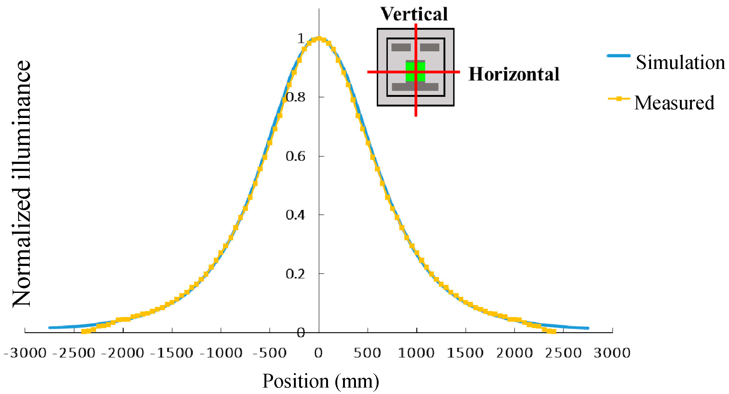
The illuminance distribution of every sample was measured by means of a digital lux meter (TES 1330A). A flat screen was utilized as a receiver at a distance of 1 m away from the sample. The emission surface of the sample, represented by the insert of Figure 7, was oriented parallel to the screen and the centers of the sample and screen were coaxial. The illuminance was measured along the central horizontal and central vertical axes on the screen. The solid curve in Figure 7 shows the normalized average of the measured data along these two axes, and the dashed curve represents the simulated illuminance after normalization. The simulated illuminance distribution agreed closely with the measured data, while a difference was noted at distances of more than 2 m away from the screen center. Because the measured illuminance beyond this distance is lower than 0.01 lux, which is beyond the accuracy of the lux meter that was used, the error is attributed to the precision of the instrument. Additionally, although the demonstrated measurement was done for an OLED with a small emission area, it is also applicable to a large surface light by extending the distance between the light source and the flat screen. Such a distance is suggested be to at least 20 times of the diameter of the emission area to geometrically restrict the angular discrepancy within 1.5°.
On the other hand, a goniophotometer (AMA LID-100) was applied to directly measure the intensity distribution. The solid line in Figure 8 provides an average intensity distribution measured along the zero-latitude and zero-longitude directions, referring to photometry type C. Additionally, from the measured illuminance distribution, the luminous intensity distribution was calculated, shown by the dashed line in Figure 8. Using the proposed model, the simulated luminous intensity distribution was obtained, represented by the dotted line in Figure 8. The curves in this figure have all been normalized to facilitate comparison. Next, the beam angles were calculated from the goniophotometer measurement, illuminance measurement, and simulation to be 127°, 124°, and 130°, respectively. The simulated curve largely agrees with the experimental data, except for instances with half angles more than ~60°. Since the locations where the discrepancies between the measured and simulated illuminances occurred are at half angles of greater than 63°, this discrepancy in intensity distribution is also attributed to the precision of the lux meter. On the whole, since the measured and simulated results are largely consistent with each other, the proposed model for investigation of illumination is acceptable.
3.5. Discussions
According to the simulated temperature distribution of the cross-section, the temperature variance for the organic layer is 2.43 × 10⁻⁴ °C. It means that the organic materials withstand a temperature gradient of 1.35 °C/mm, which is also a reference for material selection. Based on the result of temperature gradient, when the thermal parameters are known, the threshold condition of some thermal issues, such as burn-in effect, may be analyzable. Since the issues of burn-in, uniformity and lifetime in OLED display are related closely to the temperature, the proposed model is applicable to the investigation of not only the lighting but also the display application of OLED devices.
The aforementioned embodiment of the proposed model considered the structure and the parameters according to our available experimental resources. The model, though, can be utilized for other diverse conditions. A bottom-emission OLED with a desiccative layer between the Al cathode and the upper cover is taken as another example. Assume that the desiccative layer is 500 μm in thickness and filled with the nitrogen gas (N2), and the configurations of other layers are the same as aforementioned embodiment, as shown in Figure 9a. Based on the proposed modeling approach, the simulation results show that such a N2 gap brings about the maximum temperature of 33.8 °C at the upper cover, equivalent to ~2 °C higher than that of the one without N2. The reason of the temperature increment lies in the low thermal conductivity of N2, which reduces the dissipation rate of the generated heat. Then the heat accumulates in the device and causes the higher maximum temperature of the upper cover. The modelled result has reflected such a phenomenon, as shown in Figure 9b. As for the optical performance, the OLED with the N2 gap shows no significant change in simulation, compared with the one without N2. That is because those emitting rays propagating toward the N2 gap are all blocked by the Al cathode. Besides structures or configurations, OLEDs operated in altered surrounding conditions, such as a hot, cold or windy environment, can also be analyzed by the proposed model with appropriate parameters, including the ambient temperature, the convection coefficient, etc. Consequently, the proposed model is exploitable for various applications like automotive lighting and street lighting.
The proposed model utilizes plural optical and thermal parameters, such as the refractive index, the thermal conductivity and the specific heat of every layer. By means of these parameters, the model herein calculates light propagation and heat dissipation from the emitting layer through the rest layers based on the geometrical ray-tracing theory and the aforementioned heat transfer equations. Eventually, the optical and thermal performances in the air are obtained. Hence, the precision of these parameters significantly affects the accuracy of the model. Particularly, the refractive index of the organic layer is not exact but an approximate value of the integrant organic materials. Then the directions of the rays refracted from the organic layer are estimated and may cause the discrepancy between the simulated and measured optical performance. Similarly, the thermal parameters of the organic layer may incur uncertainty in the simulated thermal performance. Thus, the major limitation of the proposed model lies in the uncertain material-parameters of the organic layer, which may reduce the modeling accuracy.
Although the proposed model demonstrates only for a far-field luminous simulation, it is also able to be integrated with the near-field optical models via the algorism of the FEM, bringing about nano-scale applications. For example, along with the development of OLEDs, the optical and thermal interactions between the organic layers of an OLED device require deeper inspection. These nano-scale properties require analysis and theoretical predictions using electromagnetic-wave (EM-wave) theory without approximations. Since FEM is one of the approaches that can deal with such EM-wave issues, the proposed model, which integrates FEM and ray optics, provides compatibility for these interlayer investigations. Another example arises from the insufficient efficiency of OLEDs, while nano-techniques, such as surface plasma polaritons and graphene quantum dots [26,27,28], are investigated for new solutions. Then, there exist modeling demands for these nano-structures. Again, the light propagation through these nano-structures is out of the regime of ray-optics and has to be analyzed by means of the complete EM-wave theory. Then using FEM embedded with EM-wave equations for varying structure parameters, such as the diameter and the thickness of the nano-structures, the emission efficiency can be calculated and optimized. Afterwards, through a macro-scale model for the geometric optimization of the rest refractive structures of the OLED, the loss of the emitted light can be suppressed, and the lighting characteristics, such as luminous intensity distribution, can be designed. Thus, when the coverage of a model is extended from nano- to macro-scales, not only the efficiency of OLED devices but also their lighting performance can be optimized.
The technologies of integrated modeling of OLED devices are listed in Table 3. Each technology investigates specific performances of OLEDs. The study presented here particularly integrates the FEM thermal and ray-traced optical models for OLEDs lighting applications by means of the energy conservation theory. With the development of these modeling technologies, the designers can predict and optimize the performances of OLEDs, benefiting the reduction in both manufacturing costs and development period of the novel OLEDs.
4. Conclusions
In this study, a 3D model was constructed for analyzing and predicting the thermal effects and optical performances of an OLED lighting device. Two sub-models—an optical model and a thermal model—were integrated into a single model using a ratio of energy conversion. Compared with other OLED modeling approaches [2,3,4,5,6,7,8,9,10,11,12,13,29,30,31], the proposed model exploited the measured output radiant-power to simulate not only lighting performance, such as illuminance and luminous intensity distribution with acceptable accuracy, but also to predict the 3D temperature distribution, including that of the upper cover and that along the cross-section of the OLED devices. In addition, comparisons between the experimental and simulated results were carried out to confirm the accuracy of the integrated model. Moreover, the cross-sectional temperature of OLED devices was obtained, which provide manufacturers with guidelines for producing organic layers with appropriate glass transition temperatures, Tg. Hence, the proposed model is beneficial in not only predicting the optical and thermal characteristics of OLED lighting devices, but also designing their fabrication parameters, and even selecting materials for improving device performance.
Author Contributions
Conceptualization, methodology, project administration, and writing—review & editing, A.-C.W.; Investigation, software, validation, and writing—original draft preparation, Y.-J.H.; Visualization and software, B.-L.H.; Funding acquisition, J.-R.S.
Acknowledgments
The authors appreciate the assistance in OLED device manufacturing of Electronic and Optoelectronic System Research Laboratories in Industrial Technology Research Institute (ITRI), Taiwan, R.O.C. This study is financially supported by the Ministry of Science and Technology, Taiwan, R. O.C. under the contracts: No. MOST 105-2221-E-008-088-MY2, No. MOST 107-2221-E-008-093, and 107-2221-E-492-026-MY3.
Conflicts of Interest
The authors declare no conflict of interest.
References
- Bender, V.C.; Marchesan, T.B.; Alonso, J.M. Solid-State Lighting A Concise Review of the State of the Art on LED and OLED Modeling. IEEE Ind. Electron. Mag. 2015, 9, 6–16. [Google Scholar] [CrossRef]
- Kohári, Z.; Kollár, E.; Pohl, L.; Poppe, A. Nonlinear electro-thermal modeling and field-simulation of OLEDs for lighting applications II: Luminosity and failure analysis. Microelectron. J. 2013, 44, 1011–1018. [Google Scholar] [CrossRef]
- Gärditz, C.; Winnacker, A.; Schindler, F.; Paetzold, R. Impact of Joule heating on the brightness homogeneity of organic light emitting devices. Appl. Phys. Lett. 2007, 90, 103506. [Google Scholar]
- Slawinski, M.; Bertram, D.; Heuken, M.; Kalisch, H.; Vescan, A. Electrothermal characterization of large-area organic light-emitting diodes employing finite-element simulation. Organ. Electron. 2011, 12, 1399–1405. [Google Scholar] [CrossRef]
- Schwamb, P.; Reusch, T.C.G.; Brabec, C.J. Passive cooling of large-area organic light-emitting diodes. Organ. Electron. 2013, 14, 1939–1945. [Google Scholar] [CrossRef]
- Sturm, J.C.; Wilson, W.; Iodice, M. Thermal effects and scaling in organic light-emitting flat-panel displays. IEEE J. Sel. Top. Quantum. Electron. 1998, 4, 75–82. [Google Scholar] [CrossRef]
- Yang, L.; Wei, B.; Zhang, J. Transient thermal characterization of organic light-emitting diodes. Semicond. Sci. Technol. 2012, 27, 105011. [Google Scholar] [CrossRef]
- Poppe, A.; Pohl, L.; Kollár, E.; Kohári, Z.; Lifka, H.; Tanase, C. Methodology for thermal and electrical characterization of large area OLEDs. In Proceedings of the 25th Annual IEEE Semiconductor Thermal Measurement and Management Symposium, San Jose, CA, USA, 38–44 March 2009. [Google Scholar]
- Chen, H.T.; Choy, W.C.H.; Hui, S.Y. Characterization, modeling, and analysis of organic light-emitting diodes with different structures. IEEE Trans. Power Electron. 2016, 31, 581–592. [Google Scholar] [CrossRef]
- Park, J.; Lee, J.; Noh, Y.Y. Optical and thermal properties of large-area OLED lightings with metallic grids. Organ. Electron. 2012, 13, 184–194. [Google Scholar] [CrossRef]
- Bae, H.W.; Son, Y.H.; Kang, B.Y.; Lee, J.M.; Nam, H.; Kwon, J.H. Luminance uniformity study of OLED lighting panels depending on OLED device structures. Opt. Express 2015, 23, 30701–30708. [Google Scholar] [CrossRef]
- Bender, V.C.; Barth, N.D.; Pinto, R.A.; Alonso, J.M.; Marchesan, T.B. Scale-photo-electro-thermal model for organic light-emitting diodes. IET Optoelectron. 2016, 10, 100–110. [Google Scholar] [CrossRef]
- Kumar, M.; Gomes, J.; Pinto, A.; Pereira, L. Electro-thermal effects in large area white-organic light emitting diodes. In Proceedings of the Third International Conference on Applications of Optics and Photonics, Faro, Portugal, 8–12 May 2017. [Google Scholar]
- Ide, N.; Yamae, K.; Kittichungchit, V.; Tsuji, H.; Ota, M.; Komoda, T. Development of Extremely High Efficacy White OLED with over 100 Lm/W. J. Photopolym. Sci. Technol. 2014, 27, 357–361. [Google Scholar]
- Rakic, A.D. Algorithm for the determination of intrinsic optical constants of metal films: Application to aluminum. Appl. Opt. 1995, 34, 4755–4767. [Google Scholar] [CrossRef] [PubMed]
- Salehi, A.; Chen, Y.; Fu, X.; Peng, C.; So, F. Manipulating Refractive Index in Organic Light-Emitting Diodes. ACS Appl. Mater. Interfaces 2018, 10, 9595–9601. [Google Scholar] [PubMed]
- Moran, M.J.; Shapiro, H.N.; Munson, B.R.; DeWitt, D.P. Introduction to Thermal System Engineering: Thermodynamics, Fluid Mechanics, and Heat Transfer; John Wiley & Sons: Hoboken, NJ, USA, 2003. [Google Scholar]
- Bergemann, K.J.; Krasny, R.; Forrest, S.R. Thermal properties of organic light-emitting diodes. Organ. Electron. 2012, 13, 1565–1568. [Google Scholar]
- Haynes, W.M. (Ed.) CRC Handbook of Chemistry and Physics, 92nd ed.; CRC Press: Boca Raton, FL, USA, 2011; p. 2656. [Google Scholar]
- Qi, X.; Forrest, S.R. Thermal analysis of high intensity organic light-emitting diodes based on a transmission matrix approach. J. Appl. Phys. 2011, 110, 124516. [Google Scholar] [CrossRef]
- Watanabe, S.; Ide, N.; Kido, J. High-efficiency green phosphorescent organic light-emitting devices with chemically doped layers. Jpn. J. Appl. Phys. 2007, 46, 1186–1188. [Google Scholar] [CrossRef]
- Tanaka, D.; Sasabe, H.; Li, Y.J.; Su, S.J.; Takeda, T.; Kido, J. Ultra high efficiency green organic light-emitting devices. Jpn. J. Appl. Phys. 2007, 46, 10–12. [Google Scholar] [CrossRef]
- Baldo, M.A.; O’Brien, D.F.; You, Y.; Shoustikov, A.; Sibley, S.; Thompson, M.E.; Forrest, S.R. Highly efficient phosphorescent emission from organic electroluminescent devices. Nature 1998, 395, 151–154. [Google Scholar]
- Adachi, C.; Baldo, M.A.; Thompson, M.E.; Forrest, S.R. Nearly 100% internal phosphorescence efficiency in an organic light emitting device. J. Appl. Phys. 2001, 90, 5048–5051. [Google Scholar]
- Baldo, M.A.; O’Brien, D.F.; Thompson, M.E.; Forrest, S.R. Excitonic singlet-triplet ratio in a semiconducting organic thin film. Phys. Rev. B 1999, 60, 14422–14428. [Google Scholar] [CrossRef]
- Yu, J.; Zhu, W.; Shi, G.; Zhai, G.; Qian, B.; Li, J. Simultaneous enhancement of photo-and electroluminescence in white organic light-emitting devices by localized surface plasmons of silver nanoclusters. Nanotechnology 2017, 28, 085206. [Google Scholar] [CrossRef] [PubMed]
- Lee, I.; Park, J.Y.; Hong, K.; Son, J.H.; Kima, S.; Lee, J.-L. The effect of localized surface plasmon resonance on the emission color change in organic light emitting diodes. Nanoscale 2016, 8, 6463–6467. [Google Scholar] [CrossRef] [PubMed] [Green Version]
- Kim, D.H.; Kim, T.W. Highly-efficient organic light-emitting devices based on poly(N,N′-bis-4-butylphenyl-N,N′-bisphenyl)benzidine:octadecylamine-graphene quantum dots. Organ. Electron. 2018, 57, 305–310. [Google Scholar] [CrossRef]
- Lee, C.C.; Chang, M.Y.; Huang, P.T.; Chen, Y.C.; Chang, Y.; Liu, S.W. Electrical and optical simulation of organic light-emitting devices with fluorescent dopant in the emitting layer. J. Appl. Phys. 2007, 101, 114501. [Google Scholar] [CrossRef]
- Barnea, S.N.; Sciuto, G.L.; Hai, N.; Shikler, R.; Capizzi, G.; Wo´zniak, M.; Polap, D. Photo-Electro Characterization and Modeling of Organic Light-Emitting Diodes by Using a Radial Basis Neural Network. In Proceedings of the International Conference on Artificial Intelligence and Soft Computing, Zakopane, Poland, 11–15 June 2017; pp. 378–389. [Google Scholar]
- Pohl, L.; Kohári, Z.; Poppe, A. Vertical natural convection models and their effect on failure analysis in electro-thermal simulation of large-surface OLEDs. Microelectron. Reliabil. 2018, 85, 198–206. [Google Scholar] [CrossRef]
Figure 1.
Schematic representation of the electro-thermal simulation model.

Figure 2.
Schematic representation of the conversion between the illuminance and luminous intensity.
Figure 2.
Schematic representation of the conversion between the illuminance and luminous intensity.

Figure 3.
Green OLED sample.

Figure 4.
Average J-V curve.

Figure 5.
Measured temperature distributions of each sample. The red region in the temperature map is corresponding to the emission area of each sample with the dimension of 1 cm × 1 cm.
Figure 5.
Measured temperature distributions of each sample. The red region in the temperature map is corresponding to the emission area of each sample with the dimension of 1 cm × 1 cm.

Figure 6.
Simulated temperature distributions (a) on the upper cover glass and (b) along the central cross-section, and (c) an enlarged graph of (b). The emission area is 1 cm2 corresponding to the OLED dimension shown in Figure 3.
Figure 6.
Simulated temperature distributions (a) on the upper cover glass and (b) along the central cross-section, and (c) an enlarged graph of (b). The emission area is 1 cm2 corresponding to the OLED dimension shown in Figure 3.


Figure 7.
Measured and simulated illuminance distributions.

Figure 8.
Luminous intensity distributions derived from goniophotometer measurement, illuminance measurement, and simulation.
Figure 8.
Luminous intensity distributions derived from goniophotometer measurement, illuminance measurement, and simulation.

Figure 9.
Another embodiment of the OLED with a desiccative layer filled with N2. (a) Schematic representation of structure, and (b) simulated temperature distributions on the upper cover glass.
Figure 9.
Another embodiment of the OLED with a desiccative layer filled with N2. (a) Schematic representation of structure, and (b) simulated temperature distributions on the upper cover glass.


Table 1.
Dimensions and optical properties of the layers.
| Area (cm2) | Thickness (mm) | Refractive Index | References | Interface Property | |
|---|---|---|---|---|---|
| Upper cover (glass) | 3 × 3 | 1 | 1.5 | [14] | |
| Transparent, Fresnel equations considered | |||||
| Cathode (Al) | 1 × 1 | 1 × 10⁻⁴ | 0.96526 + i 6.3996 | [15] | |
| Reflective, Lambertian scattering | |||||
| Organics | 1 × 1 | 1.8 × 10⁻⁴ | 1.75 | [16] | |
| Transparent, Fresnel equations considered | |||||
| Anode (ITO) | 1 × 1 | 1.5 × 10⁻⁴ | 1.8 | [14] | |
| Transparent, Fresnel equations considered | |||||
| Base (glass) | 4 × 4 | 1 | 1.5 | [14] | |
*The refractive indexes of the layers referred to the data in literatures, which may cause deviations between simulated and measured results. Additionally, the refractive indexes of the organic materials in an OLED device generally range from 1.68 to 1.8 [16]. To model these integrant organic materials by one organic layer, an approximate refractive index of 1.75 is utilized herein.
Table 2.
Parameters of the layers in the thermal sub-model.
| Thermal Conductivity (W/m∙K) | Density (kg/m3) | Specific Heat (J/kg∙K) | References | |
|---|---|---|---|---|
| Upper cover (glass) | 1.4 | 2.4 × 10³ | 8.2 × 10² | [18,19] |
| Cathode (Al) | 237 | 2.7 × 10³ | 9 × 10² | [18,19] |
| Organics | 0.2 | 1.2 × 10³ | 1.7 × 10³ | [18,20] |
| Anode (ITO) | 8 | 7.2 × 10³ | 3.4 × 10² | [20] |
| Base (glass) | 1.4 | 2.4 × 10³ | 8.2 × 10² | [18,19] |
* The parameters of materials are derived from literatures and not from the measurements of the materials in use, which may results in deviations between simulated and measured results.
Table 3.
Integrated-modeling technologies for OLED devices.
| Modeling Technology | Simulation Targets | References | ||
|---|---|---|---|---|
| Optical Features | Thermal Features | Electrical Features | ||
| Successive network reduction (SURND) |
|
| [2,8] | |
| Finite-element method (FEM) |
| [3,4] | ||
| FEM + Computational fluid dynamics (CFD) |
|
| [5] | |
| Photo-electro-thermal theory (PET) + Spectral power distribution (SPD) |
| [9] | ||
| Equivalent circuits model |
| [10,11,12,13] | ||
| Doping device model + Thin-film optics |
|
| [28] | |
| Radial Basis Neural Network |
|
| [29] | |
| Vertical natural convection models |
|
| [30] | |
| FEM + Ray tracing |
|
| Proposed herein | |
© 2018 by the authors. Licensee MDPI, Basel, Switzerland. This article is an open access article distributed under the terms and conditions of the Creative Commons Attribution (CC BY) license (http://creativecommons.org/licenses/by/4.0/).
Share and Cite
MDPI and ACS Style
Wei, A.-C.; Huang, Y.-J.; Huang, B.-L.; Sze, J.-R. Integration of Optical and Thermal Models for Organic Light-Emitting Diodes. Electronics 2019, 8, 17. https://doi.org/10.3390/electronics8010017
AMA Style
Wei A-C, Huang Y-J, Huang B-L, Sze J-R. Integration of Optical and Thermal Models for Organic Light-Emitting Diodes. Electronics. 2019; 8(1):17. https://doi.org/10.3390/electronics8010017
Chicago/Turabian StyleWei, An-Chi, Yih-Jong Huang, Bo-Lin Huang, and Jyh-Rou Sze. 2019. "Integration of Optical and Thermal Models for Organic Light-Emitting Diodes" Electronics 8, no. 1: 17. https://doi.org/10.3390/electronics8010017
Note that from the first issue of 2016, this journal uses article numbers instead of page numbers. See further details here.