1. Introduction
Many recent papers have introduced interesting topologies of oscillators based on various active elements performing so-called single-resistance control of the frequency of oscillation (FO) and single-resistance control of the condition of oscillation (CO) [
1]. However, single-resistance-controllable oscillators (SRCOs) [
1] have many drawbacks resulting from their natural operation. The overall performance of the oscillator is influenced by adjusting the single integrator. It results in the dependence of the amplitude of one generated signal on the FO and the nonlinear dependence of the FO on the driving resistance value [
1]. In some cases, phase shift between generated waves is also influenced because of the fundamental principle of operation. In recent approaches, as little as two resistors can be suitable for FO control (see
Table 1); however, there is an issue with the independency of the CO when the inequality of values occurs. This issue is not solved in many works utilizing various active elements [
2]. A comparison of known solutions (references [
3,
4,
5,
6,
7,
8,
9,
10,
11,
12,
13,
14,
15,
16,
17,
18,
19]) with similar complexity (two active devices from the family of the simplest current conveyors [
2] and their modifications) is given in
Table 1.
We may formulate the following conclusions based on the analysis of items in
Table 1:
- (a)
already known solutions lack constant (not varying) amplitudes when the FO is tuned (especially SRCO solutions [
3,
4,
5,
6,
7,
8,
9,
10,
11,
12]) or this issue was not analyzed,
- (b)
many solutions [
3,
4,
5,
6,
7,
8,
9,
10,
11,
12,
15] where the first resistor serves as the FO control and the second as the CO control are not minimal (an additional resistor with a fixed value is included in the CO and FO relations simultaneously),
- (c)
the majority of already known solutions provide only inversely proportional square root dependence of the FO on the driving force (value of the single resistor, FO~R−1/2), which limits the tunability to be quite narrow,
- (d)
solutions combining control by value of passive element (or its replacement) and active parameter (for the CO control, for example) are not studied (only Reference [
14] discusses the adjustment of the CO by an active parameter; however, the FO is also tuned by an active parameter (
RX)),
- (e)
solutions implementing two parameters for FO tuning (completely uncoupled from the CO) in order to extend tunability are not proposed (with the exception of Reference [
14], where this operation was not verified),
- (f)
the simple implementation of necessary systems for amplitude gain control circuit (AGC) for amplitude stabilization utilizing electronically (voltage) controlled CO by a specific active parameter is not considered in the majority of solutions summarized in
Table 1. Therefore, many topologies have very uncomfortable CO (with a typical form of
C1 =
C2 or
R1 =
R2, and their presence is also found in the FO as product of
R1R2 and
C1C2, see for example solutions in [
17,
18]). An additional active or passive parameter suitable for the adjustment of CO (not included in the FO relation) should be included, but it cannot be revealed (in these simple solutions having 2
R, 2
C) without the analysis of general (not equal to unity) terminal transfer relations of the active elements (current conveyors).
In particular, the last problem (f) of the simplest published solutions (two active devices, 2 R, 2 C) merits attention because there is significant room for improvement in these previously published solutions, especially concerning specific types of SRCO oscillators.
Some innovative approaches to the FO tunability can be found in topologies where resistor values cannot be used for the FO and the CO adjustment due to the unsuitable form of the characteristic equation. This method supposes the replacement of the negative capacitor (s) with an electronically controllable equivalent for the purposes of FO tunability [
16]. However, the complete solution requires additional active devices (one or two) and additional passive elements (two or three). Therefore, such a solution is not minimal and the remaining drawbacks mentioned above still stand (dependence of generated amplitudes on the FO tuning and limited inversely proportional square root dependence of the FO on equivalent capacitance value—not analyzed in Reference [
16]).
The controllability of the FO by two values of resistors (completely uncoupled from the CO) is possible in topologies proposed by Soliman [
9]. However, three active devices (CCII+ and CCII−) or two dual output CCIIs (not commercially available) are required. The condition of oscillation can also be controlled by two resistors that are not presented in the equation for the FO. Note that the engagement of both resistors (suitability derived from characteristic equations) in References [
9,
14,
17,
18] for full employment in FO tuning is not supposed and tested in these works. In addition, the majority of solutions focus on a quadrature type of phase shift; different phase shifts are not expected to be obtained in these structures, but it is possible as shown in our contribution. Work presented by Bajer et al. [
19] introduced a new type of Wien oscillator. The FO cannot be simply tuned without impact on the CO if a special matching condition is not fulfilled (unfortunately, the FO adjustment was not tested). Amplitude stabilization (with the exception of many other circuits included in
Table 1) is solved by an optocoupler regulating floating resistor.
The goals of our work include the proposal of: (1) improved dependence of the FO on the driving force (extended tuning of the FO) in comparison with standard SRCO types; (2) constant amplitude ratio of generated waveforms when the FO is tuned; (3) using only grounded capacitors in topology; (4) only two active elements, only two capacitors, and two resistors employed in the circuitry; (5) simple implementation of AGC; (6) comfortable tuning of the FO by a single control voltage—a voltage-controlled oscillator (VCO); and (7) constant phase shift (45 degrees) during the tuning of the FO. Point (6) particularly requires the careful selection and testing of known methods for the replacement of the resistor with an electronically controllable equivalent. We selected a rather nonstandard method (optocoupler with resistive output stage) that has not been frequently used for these purposes in the past but brings certain advantages (no significant additional power consumption, not comparable with standard commercially available active devices, good linearity, good frequency features).
The novelty of the presented circuit is revealed by the following features: (a) values of both external resistors presented in a topology of the oscillator topology are suitable for tuning purposes; (b) permitted voltage-controlled linear tuning of frequency that is not possible in the case of many previously published and similar topologies known as single-resistance-controlled methods; (c) no further “dummy” resistors or resistors suitable for the control of the oscillation condition occur in the presented topology; (d) comfortable control of the condition of oscillation by a single active parameter (current gain) independent from frequency; (e) optocouplers with the resistive output stage offer less distorted output waveforms and more precise tuning of the frequency (even when one of the resistors occurs in the floating form) than the field effect transistor (FET), which is not easily applicable in the floating form; and (f) the method of electronic control (voltage driving of optocouplers) improves the ratio of the frequency readjustment (tuning) vs. the driving force ratio.
This paper is organized as follows:
Section 1 introduces the topic of resistance-controllable oscillators and provides an overview of significant solutions and their features with respect to our intentions in the above defined goals.
Section 2 compares the parameters and available features of the two most similar solutions and our proposal in detail.
Section 3 discusses reasons for the selection of the implemented method of resistance control.
Section 4 analyses the discussed solution of the oscillator (features of controllability).
Section 5 provides a precise explanation of the design and features of the component parameters as well as the experimental results of the circuit behavior when the FO is tuned and their comparison to the expectations and ideal theory. Further methods of the indirect electronic tunability (replacements of resistors) are briefly evaluated and compared in
Section 6.
Section 7 concludes this work.
2. Detailed Qualitative Comparison of the Most Similar Solutions and the New Proposal
The following section explains the main differences of the newly proposed circuit and the most similar solutions (topologically) already presented. Kumngern et al. [
14] proposed a similar topology of the oscillator where the target adjustability of the FO was solved by driving the intrinsic resistance of the input terminal
X (
RX) by the bias current. This means that external resistors are not present in the solution [
14]. Unfortunately, current conveyors with controllable internal resistance
RX are not available on the market. The control of the bias current (in order to adjust
RX) also has a significant impact on the frequency bandwidth (transfer
Y→
X), input dynamics, and linearity as well as the output resistance of the current conveyor (unintentional but unavoidable) [
20]. Then, the range of
RX value can be very limited. This results in a reduced range of FO tunability. Therefore, our contribution, by solving the tunability of the FO with external replacements of both resistors, brings improvement to the common practice (especially owing to the very low ratio of the driving force vs. the ratio of FO readjustability, see
Table 2). The CO in Reference [
14] also proposes adjusting by the bias current, setting a gain between the
X and
Z terminals of the current conveyor. Unfortunately, the implementation of the topology as a two-phase oscillator as well as the analysis of the output relation has not been performed and only a single-resistance
RX was employed for the FO tuning. This results in an inversely proportional square root dependence of the FO on
RX, i.e., limited tunability. Therefore, the full potential of the topology was not revealed and tested in Reference [
14]. A very low output amplitude (only slightly more than 20 mV) was also obtained in the results of Reference [
14]. Our solution offers a larger output level (amplitudes more than 100 mV). All these aspects (and more details) are clearly visible in
Table 2. Lahiri [
17] proposed a very similar (topologically) circuit (Figure 1a in Reference [
17]), producing output signals in current form. However, the topology also had high-impedance nodes where the output voltages were presented. Several features, compared in
Table 2, are similar to those of Reference [
14] and our proposal (number of active and passive elements, character of allowed and tested FO dependence). Nevertheless, the range of tested tunability is very narrow (narrow change of resistance value = low ratio of FO readjustability), CO cannot be electronically controlled, and the generated levels are not independent from the tuning process. Other similar solutions (listed in
Table 1) do not provide detailed information about the features required for the comparison in
Table 2. Therefore, other solutions are not included in this detailed comparison (
Table 2).
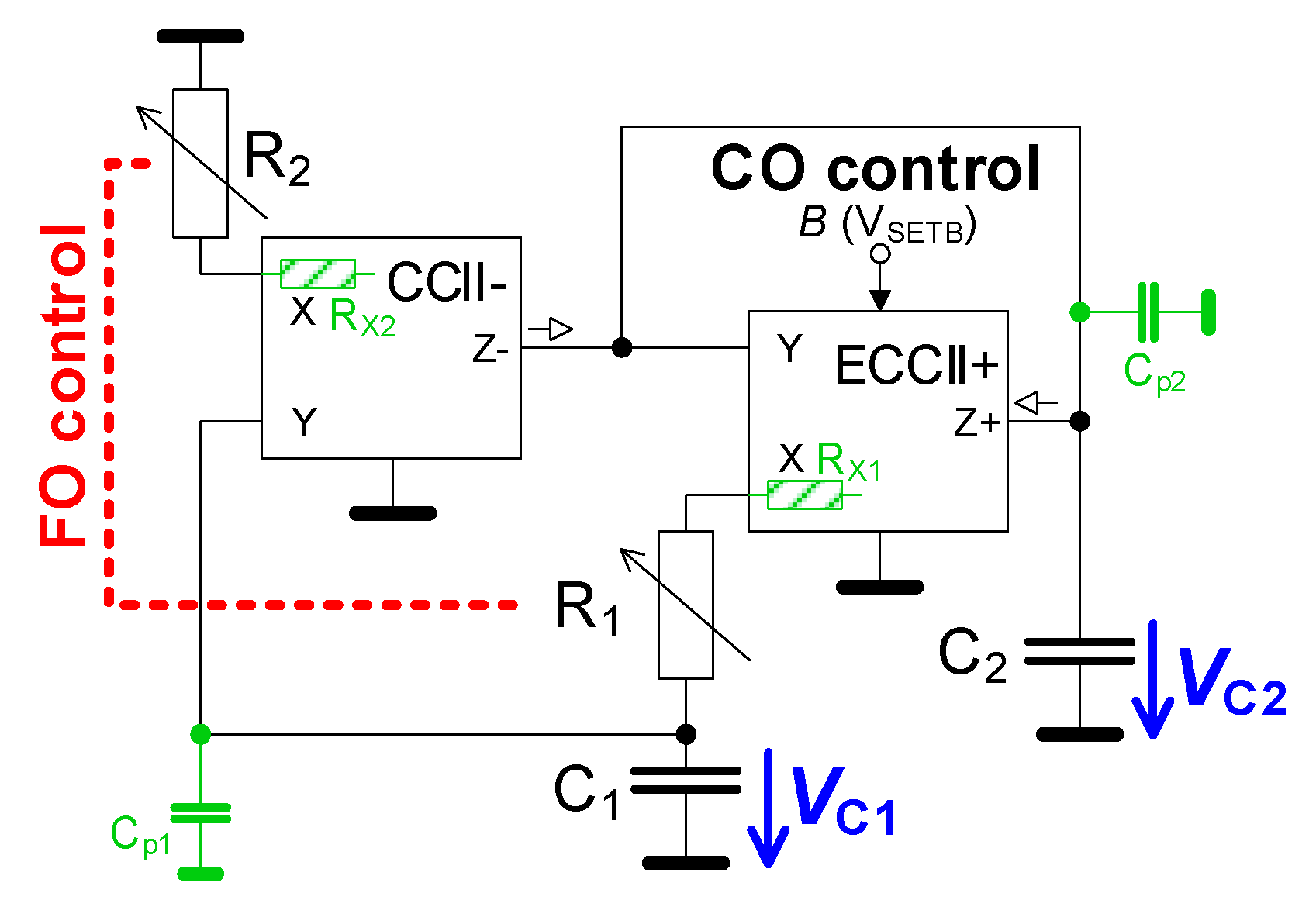
4. Topology Suitable for Selected Method of FO Control
Figure 1 shows the topology of the oscillator utilizing only two active devices, two grounded capacitors, and two resistors (the most similar solution [
14] omits external resistors with full consideration of the issues discussed in a previous text). The negative current conveyor of the second generation (CCII−) [
2,
22] as well as a positive electronically controllable CCII (ECCII+) [
2,
22,
23,
24,
25] have identical definitions of two inter-terminal relations—
IY = 0,
VX =
VY—whereas the most important difference rests in the transfer of the current from the
X to
Z terminals (
IZ = −
IX for CCII− and
IZ =
B∙
IX for ECCII+). The parameter
B represents a generally adjustable current gain. The characteristic equation of this simple oscillator is:
This characteristic equation offers a very beneficial condition for oscillation B ≥ C2/C1. The most important advantage of the solution results from the mutually independent CO and the FO, completely defined by the values of both capacitors and resistors having the typical form of ω0 = (R1R2C1C2)−1/2.
The relation between the generated output voltage levels (amplitudes) can be expressed as:
which can be modified into:
Supposing the equality of both resistors and capacitors (
R1 =
R2 =
R,
C1 =
C2 =
C), the previous relation can be simplified to:
The proposed oscillator theoretically offers a constant level of output amplitudes with a constant ratio of 0.707 between the generated waveforms and a phase shift of 45 degrees, while the FO is tuned by
R1 and
R2 simultaneously. Note that the controllability of the FO by a single value (
R1 or
R2) causes amplitude and phase shift changes (when the FO is tuned). Valuable engagement of both resistors for the FO control is not a typical feature in such simple circuitries (
Figure 1). This represents a very important finding in comparison with standard SRCOs and other solutions [
1,
3,
4,
5,
6,
7,
8,
9,
10,
11,
12] tunable by a single parameter value only. Moreover, the dependence of the generated output level on the tuning process (variation of the parameter intended for the FO tuning) presents an unwanted secondary effect of the single-parameter controllability of the FO [
26]. It brings additional issues with amplitude limitation and distortion. In our case, this was not an issue.
The most important small-signal parasitic effects of real circuitry (indicated by green color in
Figure 1) are easily taken into account in a modified form of Equation (1) where the parasitic (stray) nodal capacitances
Cp1,
Cp2 (in parallel to
C1,
C2) and resistances
RX1,
RX2 of the current input terminals (in
X of both current conveyors) are considered:
This equation was gained by the routine analysis of an autonomous circuit including the most important parasitic elements in
Figure 1 (indicated by green color). The new CO and FO expressions (difference from ideal CO and FO indicated in superscript
*) can be derived from Equation (5a) as follows. The equation for
ω0 * (5c) provides the expected values of FO used in Equation (8) and shown in
Table 3 when the oscillator is tuned. The relative sensitivity of the FO to the main parameters (
R1,
R2,
C1,
C2), in an ideal case derived from (1), reaches a typical value of −0.5. The sensitivities of the FO, including the effect of important parasitic parameters presented in (5c), are:
SR1ω0 * = −
R1/[2∙(
R1 +
Rx1)],
SR2ω0 * = −
R2/[2∙(
R2 +
Rx2)],
SC1ω0 * = −
C1/[2∙(
C1 +
Cp1)],
SC2ω0 * = −
C2/[2∙(
C2 +
Cp2)],
SRx1ω0 * = −
Rx1/[2∙(
R1 +
Rx1)],
SRx2ω0 * = −
Rx2/[2∙(
R2 +
Rx2)],
SCp1ω0 * = −
Cp1/[2∙(
C1 +
Cp2)]. In fact, these sensitivities have absolute values lower than those of the ideal case (<0.4 numerically for particular values from our design).
Note that many commercially available types of current conveyors have very high (MΩ) resistances (real parts of voltage inputs and current outputs) at the
Y and
Z terminals [
27] and their inclusion to (5a) does not create a significant effect in comparison with the
Cp1,2 and
RX1,2 in this case. However, there are solutions where these effects cannot be omitted and full consideration of all parasitic features must be provided for the accurate estimation of behavior at high frequencies and when the value of
C1,2 is set in hundreds of pF or lower. The specific values of
Cp1,2 for our case are discussed in the next section.
5. Design of Oscillator and Results of Experiments
The initial design of this circuit supposes
C1 =
C2 =
C = 47 pF. Note that this selection (tens of pF) is generally required in combination with resistance values (
R1 =
R2 =
R) in hundreds of Ω for the operation of this and similar oscillators above 1 MHz. However, the values of working capacities are not far from the values of stray capacitances of circuitry including the terminal capacities of active devices (units of pF). The internal value of
X terminals of CCIIs (
RX1,2) must also be taken into account from Equation (5a) and (5c). The current conveyors used in our topology (
Figure 1) are established by current-mode multipliers EL2082 [
27] and a high-speed single-input single-output transconductance amplifier known also as a diamond transistor OPA615 [
28]. The electronically controllable gain
B (proportionally driven by
VSETB voltage:
B ≅
VSETB for
VSETB ≤ 2 V [
27]; because
B ≅
k∙
VSETB, where
k = 1 [V
−1] is valid for
VSETB ≤ 2 V) of EL2082 was set to
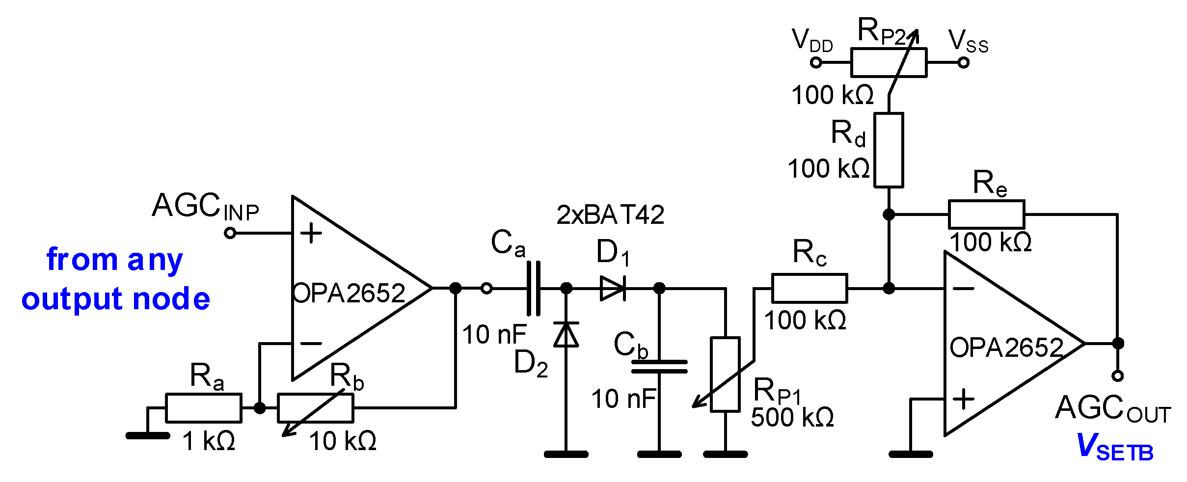
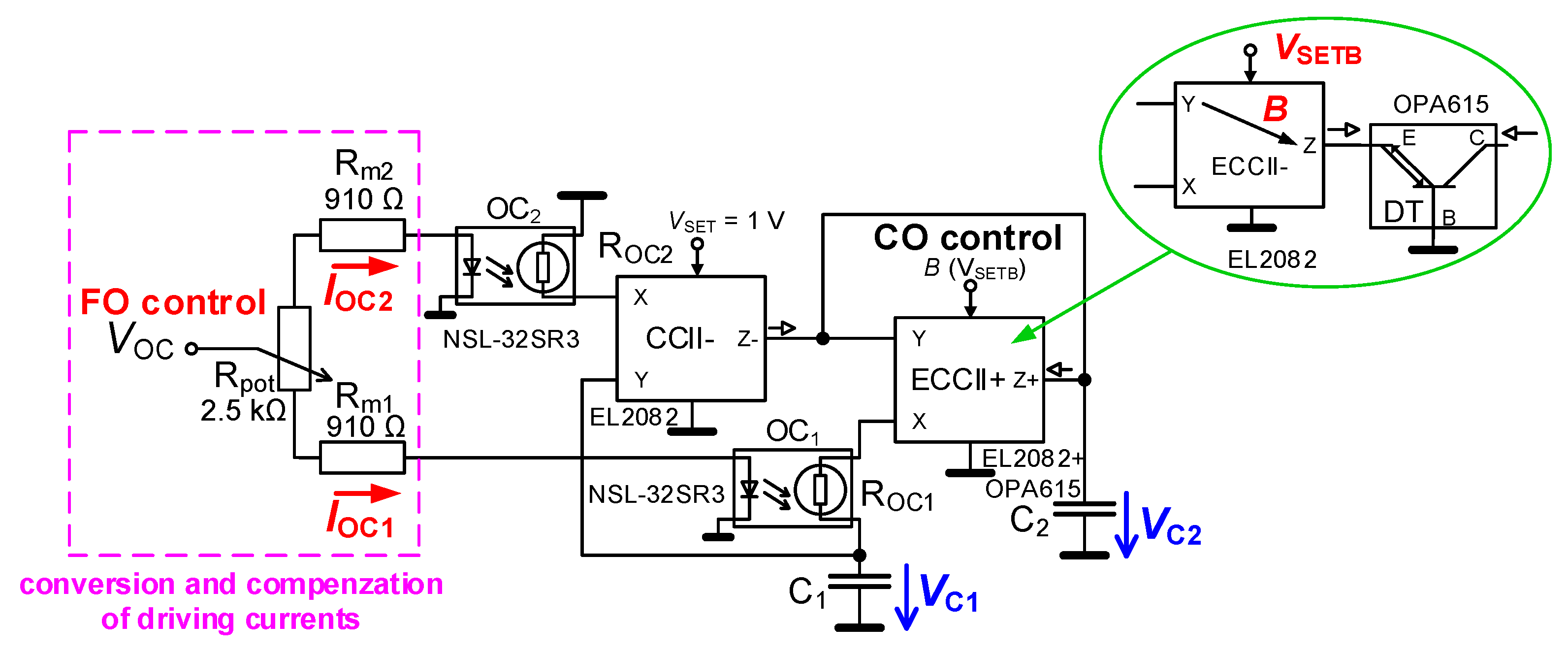
B = 1 for CCII− operation. The cascade of EL2082 with OPA615 (output inversion of CCII−) creates ECCII+ type where
B can be controlled to drive the CO by an external AGC for the amplitude stabilization of the generated waveforms (
Figure 2). The main purpose of the AGC consists in the sustentation of unchangeable output levels when the oscillator is tuned. This feature cannot be simply obtained when the CO is set to fulfill an analytically obtained relation because energetic (gain) proportions in the circuit are influenced by tunability. The operation without AGC leads to issues with output waveforms (damage of the shape by nonlinear transfer responses of active devices or even limitation), resulting in high total harmonic distortion (THD) (increased level and amount of higher harmonic components and increased level of spurious combination products) or fading (drop down) of oscillations. Voltage buffers (not included in the simplified schemes), based on the OPA2652 [
29] operational amplifier, are added to high-impedance nodes for the impedance separation and subsequent measurement of the circuit on a printed circuit board (PCB) by a low-input-impedance (50 Ω) spectrum analyzer HP4395A and oscilloscope Rigol DS1204B.
Expected values of stray/parasitic capacitances are
Cp1 = 3 pF and
Cp2 = 10 pF (in parallel with
C1 and
C2) where
Cp1 includes the
Y terminal capacity 2 pF (CCII−) [
27] and input capacity of voltage buffer (1 pF) [
29]. The estimated effect of
Cp2 supposes a capacity of 5 pF of the
Z terminal (CCII−) [
27] and the
Y,
Z terminals (2 + 2 pF) of ECCII+ [
28], as well as the input capacity of the voltage buffer (1 pF). Terminal
X has an expected input resistance
RX1,2 = 95 Ω [
27].
FO tuning can be achieved by the variation of R1 and R2 values simultaneously by a dual-channel tandem potentiometer. Our design intention targets tunability in the approximate range of 1–10 MHz. The discussed method (potentiometer) is not very comfortable for standard applications. Many systems produce a DC driving voltage or current (after D/A conversion). Therefore, we seek useful methods of indirect electronic control. The following paragraphs deal with the possible improvement of the circuit to VCO.
The position of the
R1 resistor in the topology (
Figure 1) of the oscillator requires the implementation of controllable resistance in a floating form. The replacement of
R1 by the emulator based on active devices, for example, operational transconductance amplifiers (OTAs) [
30,
31], brings significant additional power consumption, area, and further complications. Therefore, we selected the optocoupler NSL-32SR3 [
32] (photodiode-photoresistor) with very favorable features (frequency bandwidth and linearity) in a grounded or floating form in comparison with many active solutions (unipolar transistors in a linear regime). Our circuit (
Figure 1) employs two optocouplers as shown in
Figure 3.
The reasons for the presence of
Rm1,2 = 910 Ω and
Rpot = 2.5 kΩ result from the required transformation (
Rm1,2) of the driving voltage
VOC to currents with a maximal allowed value (here approximately 1.5 mA per branch, which is approximately more than 10 times lower current consumption than opamp or CCII per single supply branch, for
VOC = 5 V—fully positive supply voltage) and the compensation for the slight inequality of the resulting
ROC1 and
ROC2 (given by fabrication mismatch) for the same driving current. We compensated this effect by the slight inequality of driving currents (
IOC1 ≠
IOC2). The threshold voltage
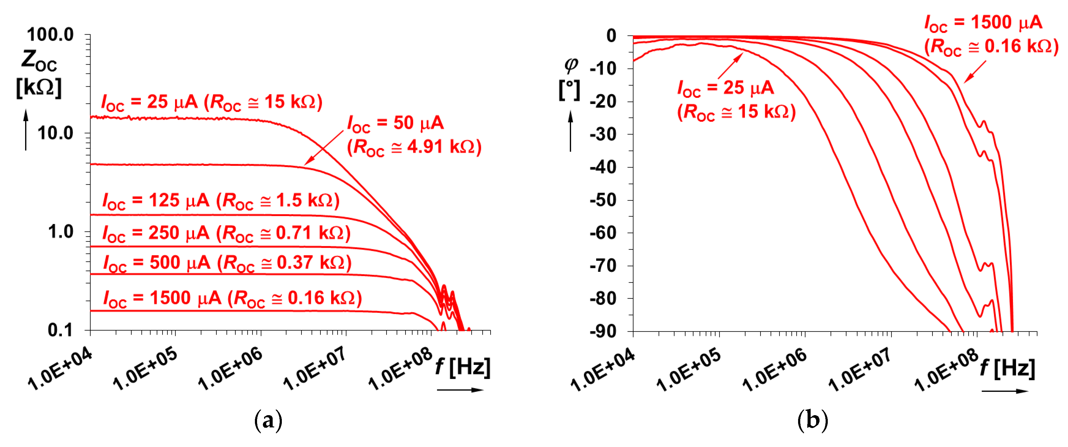
Vth ≈ 1.6 V of the optocoupler’s LED was obtained experimentally. The measured frequency features (by vector network analyzer E5071C) of the optocoupler output (
ZOC) are introduced in
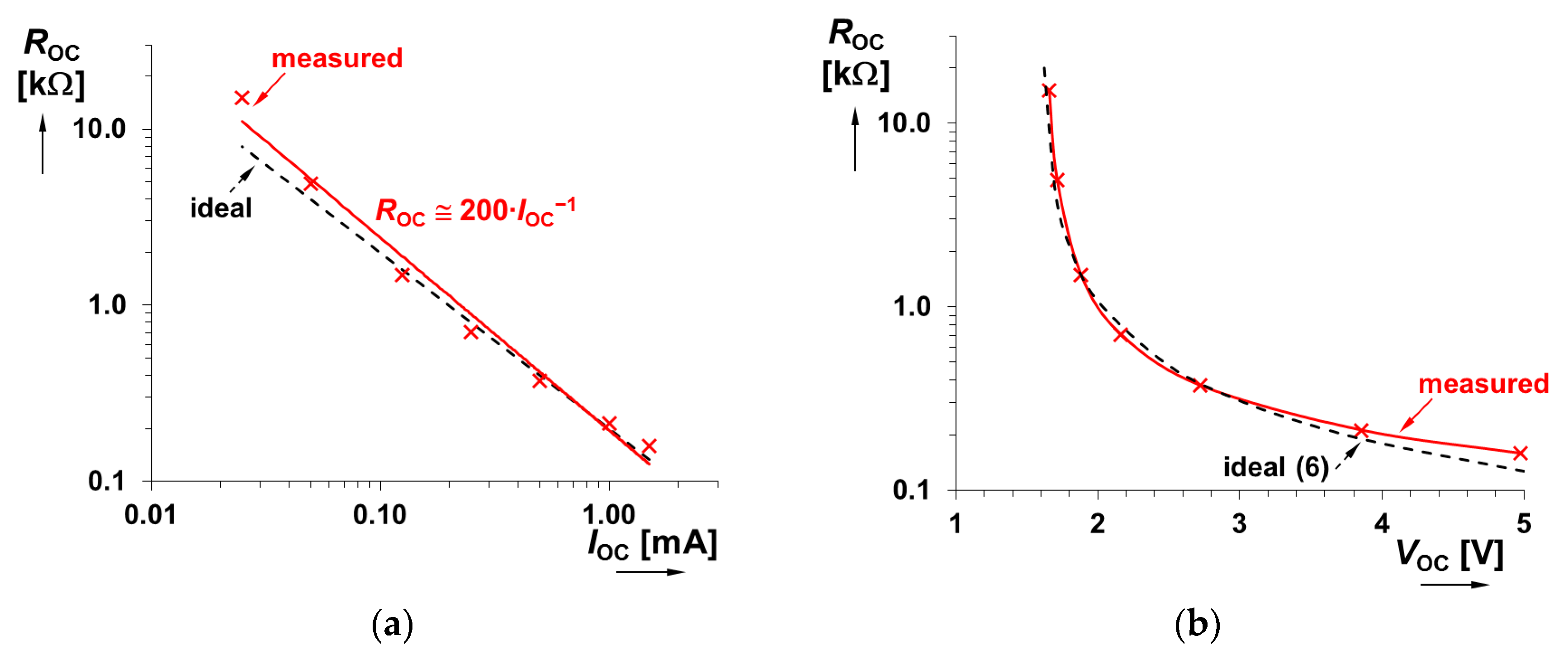
Figure 4 for particular values.
Figure 5 shows the dependence of
ROC on the driving current and voltage (in accordance with the driving circuitry in
Figure 3). The datasheet [
32] does not publish these features, but they must be known for the design of applications. Features of the device limit its implementation to systems operating around 10 MHz when the value of
ROC is set below 500 Ω. Based on our experiments, the relation between
ROC and the driving current
IOC can be found empirically as
ROC [Ω] ≅ 0.2/
IOC [A]. Then
ROC can be approximately expressed, in dependence on the driving voltage
VOC, as:
Neglecting the discussed inequality of
IOC1 ≠
IOC2, the ideal equation for the FO (
f0i) controlled by the optocoupler can be written as:
Note that this equation supposes the identical behavior of both optocouplers. A more accurate relation (especially for operations with very low values of
C1,2; above 1 MHz) for the FO (
f0e) can be obtained for real values of parasitic features included in Equation (5c). We expect identical values
RX1 =
RX2 =
RX = 95 Ω (and
Cp1 = 3 pF,
Cp2 = 10 pF) in the following expression:
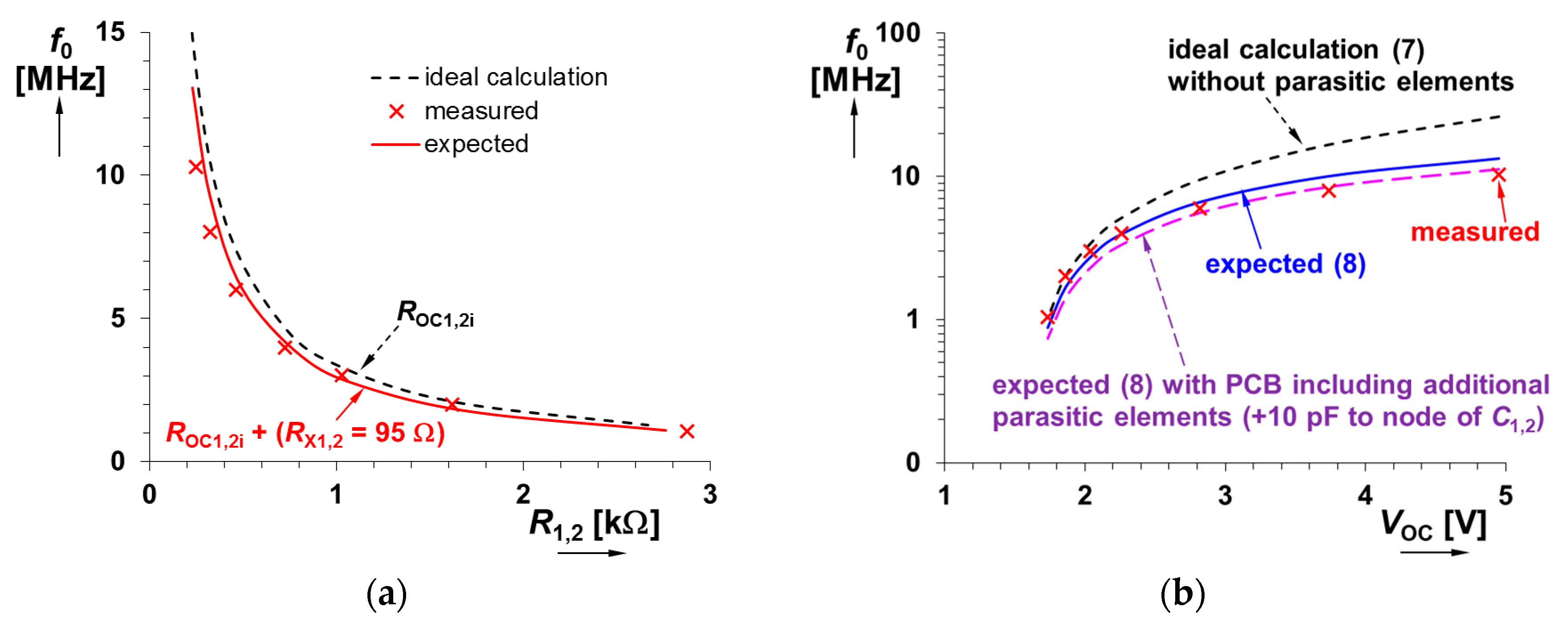
The experimental results of the FO of the oscillator in
Figure 3, including the AGC from
Figure 2, are summarized in
Table 3. The implemented optocouplers offer a range of
ROC adjustability, from approximately 130 Ω to 2.7 kΩ (
IOC varied from 75 μA to 1500 μA) in the ideal case and from 150 Ω to 2.8 kΩ in the measured case, see
Table 3 for the detailed results. The expected trace includes the abovementioned parasitic elements. These results are represented graphically in
Figure 6a, and the FO dependences for the driving of the oscillator by
VOC voltage are shown in
Figure 6b. The traces in
Figure 6b represent the ideal (Equation (7)), expected (Equation (8), including the nodal parasitics of the circuit), and the additional nodal capacitances (10 pF) expected in the case of the real printed circuit board. Finally, the measured results are very close to the case in which PCB parasitics are considered. The CO for the influenced circuit (as derived in Equation (5b)) is fulfilled theoretically for
B ≥ 1.12.
There are several reasons for the differences between the ideal, expected, and experimental behaviors (results of frequency dependences on
VOC in
Table 3 and
Figure 6b): (a) parasitic elements (capacities) of the active element due to the close values of the working capacitors to the stray capacitances; (b) transit features of active devices (their phase responses are especially important for oscillators—these issues occur at frequencies lower than −3 dB cut-off or transit frequency); (c) Miller effect of the increasing input capacity of active devices (amplifiers) when the gain is varied—the “parasitic capacity” increases with increasing gain of blocks of the circuit; this behavior is not easily predictable and implementable to the design equations; (d) high uncertainties in bands above 1 MHz given by real parasitic features of the PCB (parasitic conductivity, inductance, and capacity) that can be only approximately estimated in the case of capacity—the accuracy and high-frequency (RF) behavior of circuits operating above 1 MHz highly depends on the design and quality of the PCB; and (e) inequality of the driving current of optocouplers (
IOC1 ≠
IOC2).
The ideal calculation (ideal values of C1,2 and ROC1,2) supposes a range of the FO tunability of 1.04 MHz→25.27 MHz. Calculations including all important parasitic effects estimate a range of 0.89 MHz→13.32 MHz (R1,2 varied from 247 to 2.88 kΩ). Consideration of the additional PCB effect (+10 pF) leads to a range of 0.75→11.21 MHz. The experimental values follow our expectations because the measured FO yields a range of 1.05→10.30 MHz.
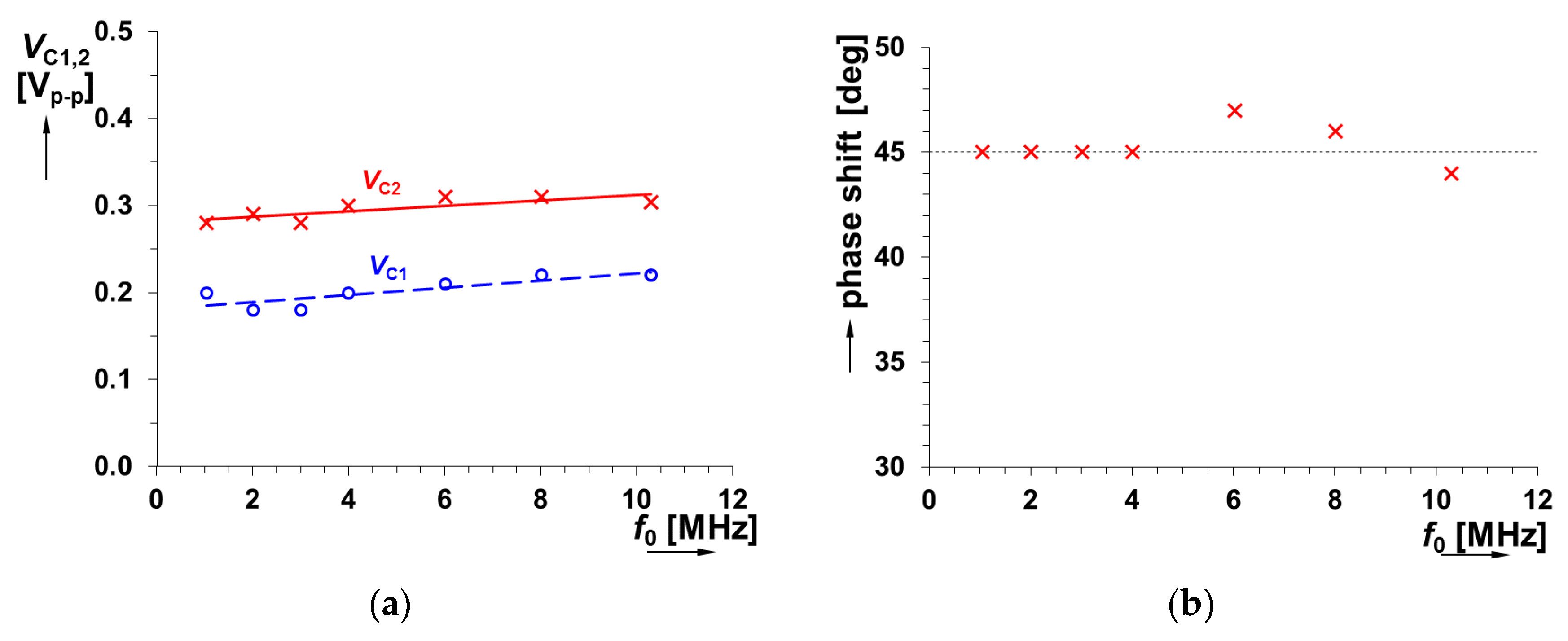
Output amplitudes (
VC1 and
VC2) reach levels of about 200 mV
p-p and 300 mV
p-p (based on the setting of the AGC) and they remain almost constant during the tuning process (
Figure 7a). Their ratio confirms the validity of Equation (4). The phase shift of both signals is around 45 degrees (
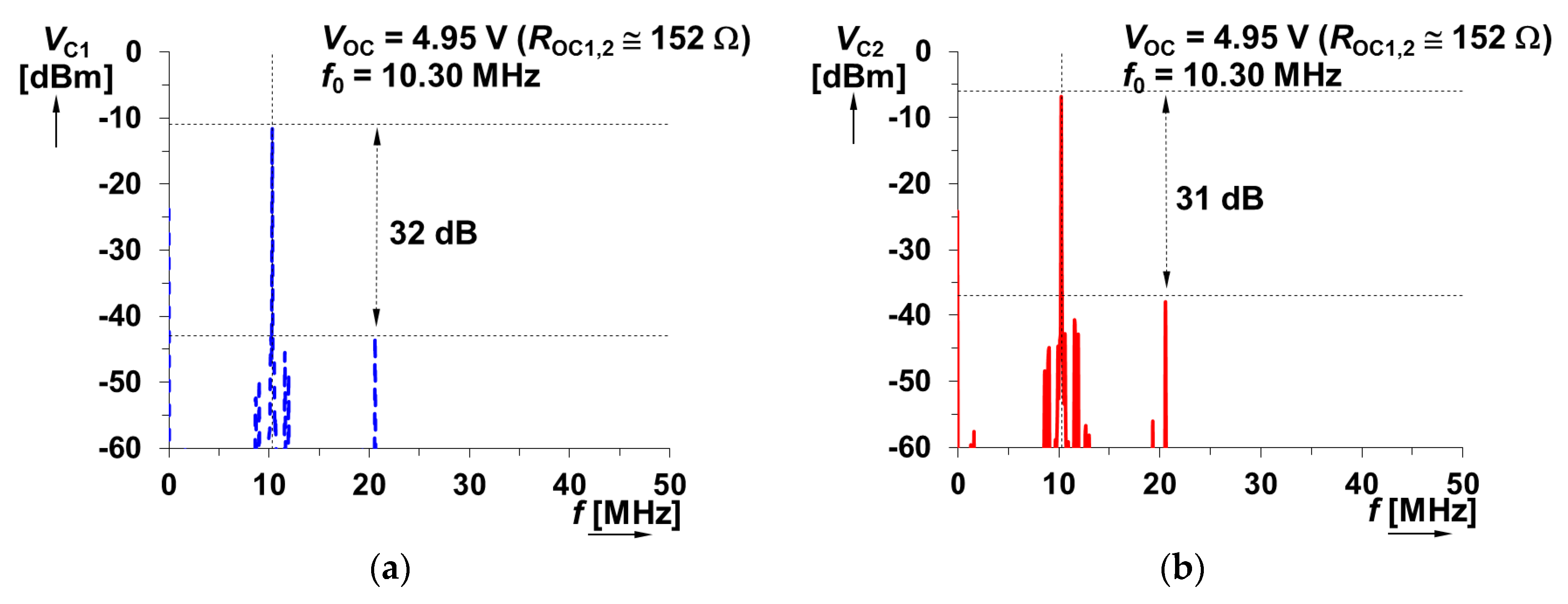
Figure 7b). This value was obtained from the oscilloscope in the time-domain measurement by the automatic function evaluating the distance at which signals at both channels cross 0. An example of transient responses for
VOC = 4.95 V (
f0meas = 10.30 MHz) is shown in
Figure 8. Their spectral analysis provided the results shown in
Figure 9. The THD varies between approximately 0.7 and 3.3%. Quite high values are given by the low suppression of higher harmonic components of the active device itself (especially by the high-speed device OPA615 [
28], only about 35 dBc in MHz bands). Similarly, the implementation of many nonlinear high-speed devices results in a certain presence of somewhat influential intermodulation products (visible in transient responses as superposed fluctuations at peaks of amplitudes as well as some combination products observed in the spectral analysis around the fundamental tone). The overall power consumption of the testbed (including buffers and opamps in AGC) reaches 570 mW (five IC devices, approximately 60 mA of power current per supply branch, ±5 V).
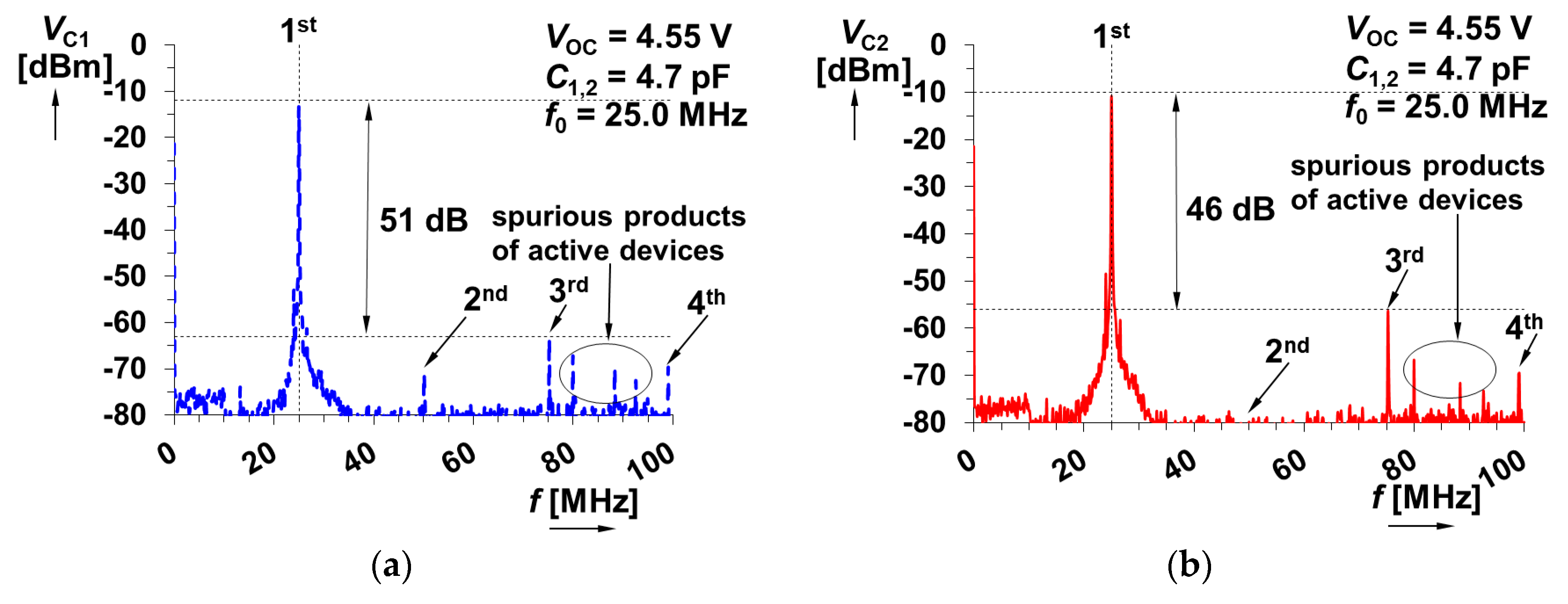
We replaced values of capacitors in the oscillator in order to demonstrate the maximal available FO in the experimentally tested prototype for a still practically feasible value (
C1,2 = 4.7 pF was selected). Then, the value
f0 = 25 MHz was set experimentally by
VOC = 4.55 V. The results of the spectral analysis are shown in
Figure 10 for both output waveforms. Images of the measured prototype are given in
Figure 11.
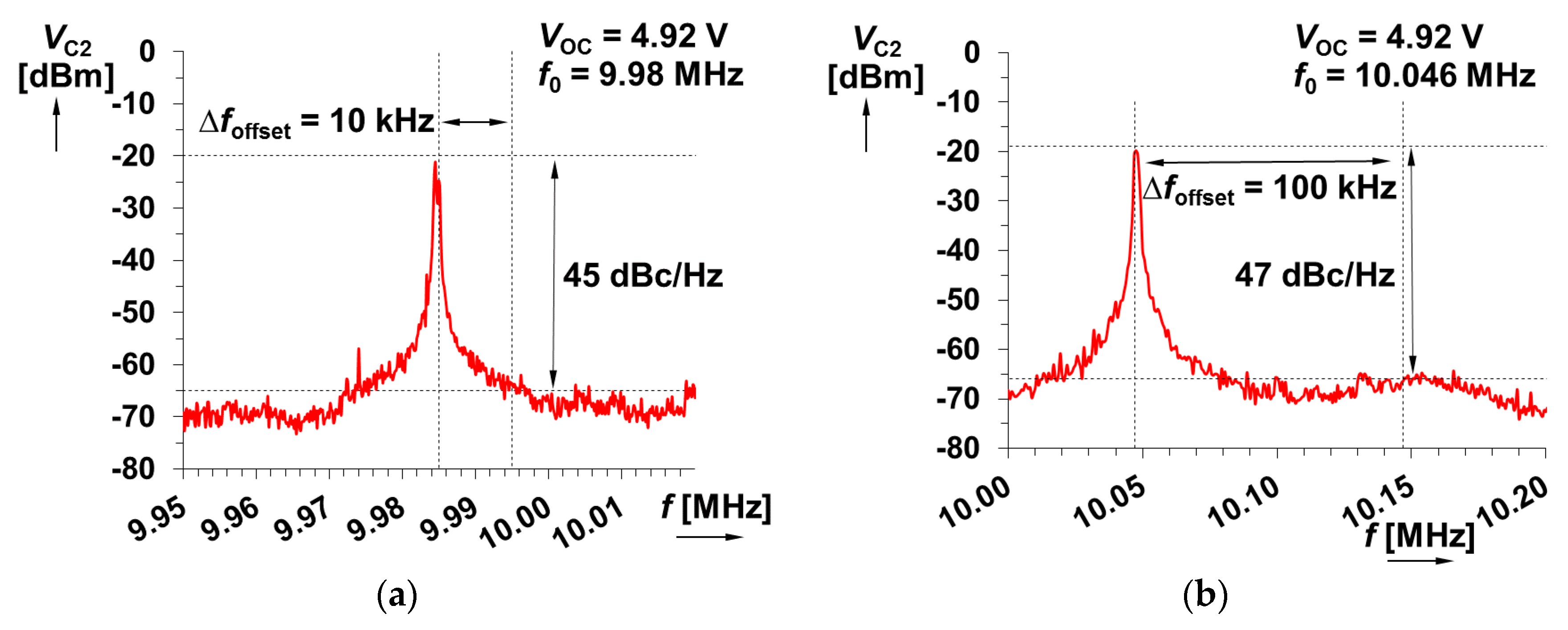
The phase noise evaluation is shown in
Figure 12 for
VC2 output (these values are actually almost identical for both outputs). The phase noise value was obtained for offset frequency ∆
foffset = 10 kHz and 100 kHz (1/1000 and 1/100 of fundamental tone; the oscillator frequency was set to
f0 ≅ 10 MHz by
VOC = 4.92 V for this test). The phase noise values of 45 and 47 dBc/Hz were obtained for these values of offset frequencies. Note that these are only approximate values due to the limited accuracy of measurement (the noise background is influenced by the resolution-bandwidth (RBW) of the spectrum analyzer that was set to 10 Hz in all cases). The value in the range of 40→70 dBc/Hz is typical for these types of circuits due to the usage of inertial AGC (it solves limitation, shape distortion, THD, and the variation of output levels when
f0 is tuned, but its drawback is the higher fluctuation/jitter of output amplitudes). Radio-frequency (GHz)-targeted solutions reach values in the high tens of dBc/Hz (for example >100 dBc/Hz) in dependence on ∆
foffset because there is no AGC system in narrow-band tunable oscillators and higher spurious spectral products are filtered. However, this approach cannot be used in base-band or inter-frequency-band oscillators tunable in the
f0 range of 10:1 or more. Note that the phase noise and
f0 stability (except AGC) also depend on the precision of the construction of the circuit (quality of the PCB, etc.). It may significantly influence overall performances, especially at high frequencies above 1 MHz. The fundamental tone slightly fluctuates in the results shown in
Figure 12. The frequency change achieves ±33 kHz (±0.33% at
f0 ≅ 10 MHz), which results in a frequency stability of
S(
f0) = |∆
f0/
f0| = 6.6 × 10
−3 (being within the typical range for active RC oscillators).
6. Discussion of Other Methods of Indirect Electronic Control of FO
The position of the resistor
R1 is not very beneficial due to the floating (between two nodes) connection to the circuit. The method discussed in the previous paragraphs implemented optocouplers; however, there are also other possibilities that should be briefly discussed (their main advantages and disadvantages).
Table 4 reveals their general comparison.
The replacement of
R1,2 by junction field effect transistors (J-FET) in a triode/ohmic/linear regime [
11,
12,
33,
34,
35] can be easily applied. However, there are some restrictions. It is not easy to maintain a transistor in a linear regime (
VDS <
VGS −
Vth) even for increasing processed signal levels in nodes where transistors are connected. Transistors behave highly nonlinearly for voltage levels higher than several tens of mV, and nonlinearity increases for increased resistance (
rDSon) driven by
VGS voltage. The range of the
rDSon resistance adjustability can be large (N type J-FET BF245A [
36]: 200 Ω→2 kΩ for 0→−2 V); however, the nonlinearity of
VDS vs.
ID plots plays a significant role, especially for high values of resistances (high
VGS). Unfortunately, there is no other way in the IC design practice. One example of J-FET implementation was experimentally tested in our oscillator (
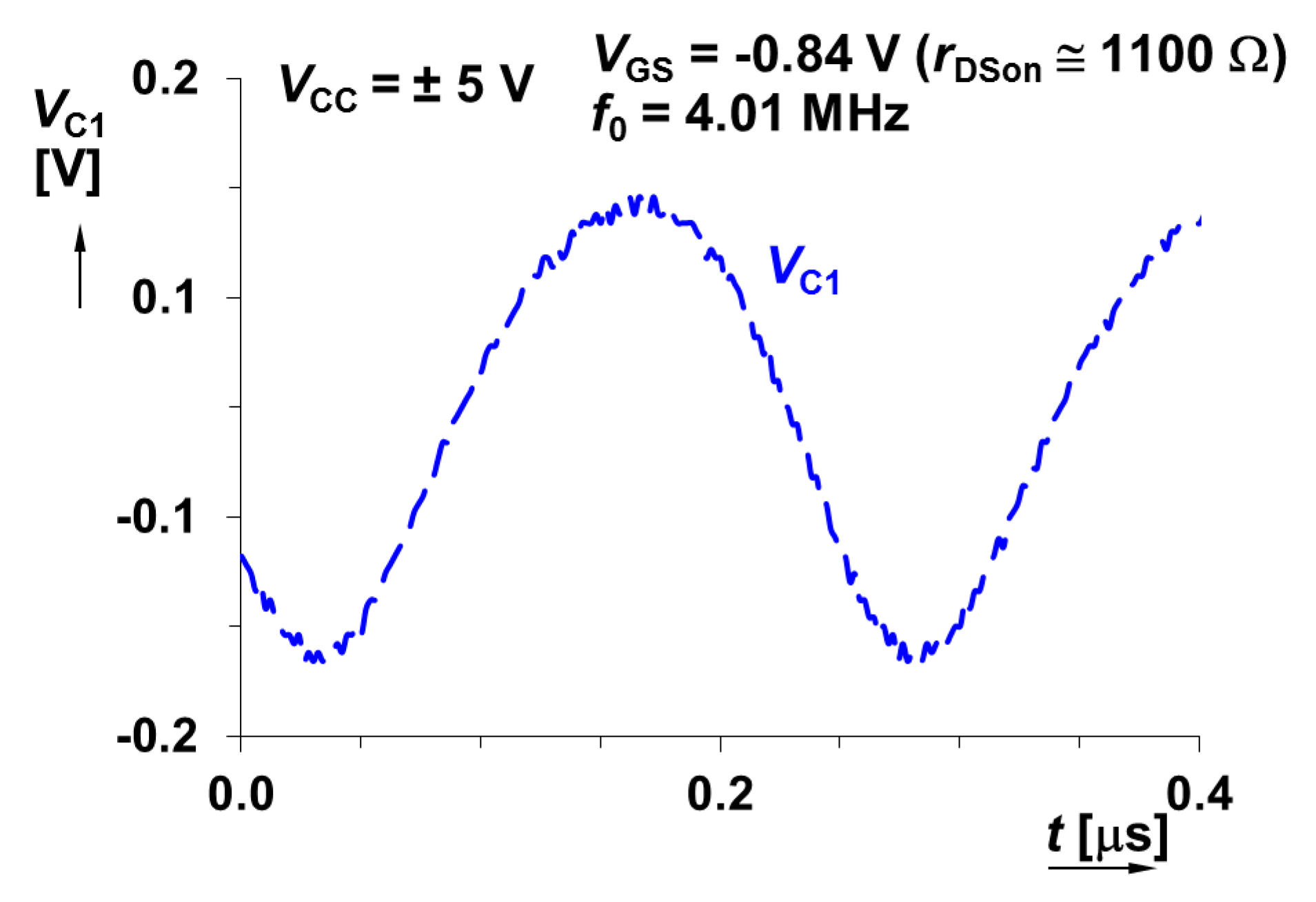
Figure 1).
Figure 13 illustrates the output level for the
VC1 wave that is significantly distorted (THD > 13%) by nonlinearity with increased values of
rDSon. The amplitude is not limited but the shape and symmetry of the positive half-wave vs. negative half-wave is significantly damaged. The linearization of the transistor can be provided by two additional resistors [
33]; however, the linearization of the floating form of an electronically controllable equivalent is not an easy task (many additional active and passive devices are required) [
34,
35].
Digital potentiometers [
37,
38,
39,
40] are widespread parts serving in control and adjustable systems, especially for low-frequency circuits. They have the advantage of simple digital controllability of value; however, many drawbacks limit their practical usability in medium- and high-frequency systems. These issues consist in real parasitic resistance of the middle terminal (wiper), large parasitic capacitances (tens of pF), and therefore very bad frequency features (only tens–hundreds of kHz in many cases). Discontinuous adjustment of the value (based on the number of bits) can be also considered as a drawback for specific applications (the control of amplitude stabilization, for example). Also, the reaction on changes (depending on the construction of specific types and their internal control logic) can be very slow. Therefore, the majority of these devices are unsuitable for the FO tuning in the range presented in this paper.
Similar features are offered by D/A converters (they can establish controllable resistors [
41]). However, modern and very fast (Gsps) solutions can be prepared for high-frequency operation. Unfortunately, the power consumption is enormous (power supply currents in hundreds of mA) and the price reaches tens of dollars. This renders this method unsuitable for compact designs and solutions.
Active solutions (a floating resistor can be implemented by two OTAs [
30,
31]) may have a very good frequency response and fast reaction on changes (adjusting of the driving voltage). However, active solutions (especially OTA-based solutions without linearization [
30]) have substantial problems with linearity and dynamical restrictions. The range of the equivalent resistance value can also be very limited (especially in MOS solutions where square laws [
42,
43] for currents are valid).
The following discussion evaluates the features of the proposed analog solution and direct digital synthesis (DDS). Advantages of DDS are clear: wide bandwidth (hundreds of MHz), simple configurability, stable operation, excellent phase noise (but this parameter is significant for bands starting at hundreds of MHz, not for the bands observed in this paper), immunity to aging of parameters, minimized temperature effects, high accuracy, etc. On the other hand, many DDS chips generate only single-phase waveforms (70–80% of production). The generation of more than one waveform requires the interconnection of several chips or multichannel DDS (conferring a significantly higher power consumption and cost). DDS chips require an external clock generator (additional complication and power consumption) in some cases. The frequency is not continuously tunable. The power current reaches hundreds of mA. A DDS must be equipped with some microcontroller and/or supporting peripheral devices (USB connection, interface, clock generator = additional power consumption), or DDS development boards are used in many designs (several times higher cost). The cost of the complete designed analog oscillator in this paper (elements used in implementation) reaches approximately 30 Euros, the cost of the multichannel DDS (AD9959 for example) chip (with only the chip ready for implementation) reaches 40 Euros, and the cost of the complete operating development board with DDS is several times higher (approximately 350 Euros). Therefore, advantages coming from the utilization of DDS can be overcome by a low-cost solution with acceptable features for the intended application.
The main advantages of the proposed analog solution in comparison to DDS are: (a) simplicity of the resulting circuit and tunability method (an integrated DDS has a much more complex block topology and a higher complexity of internal blocks—it cannot be implemented in discrete form in practice); (b) low cost (for the intended bandwidth—up to low tens of MHz); (c) immediate response of frequency on changes (no delay); (d) no requirement for additional peripheral devices (clock generator, interfaces, etc.); (e) no requirement of programming (the approximate final costs noted above do not take the controlling software for multiphase generation and the tuning of the DDS into account). Of course, there are also disadvantages: (a) influence of temperature and aging effects on frequency stability; (b) low value of phase noise and worse stability (however, this issue is usually not evaluated/solved in the case of similar solutions in studied bands of units—low tens of MHz); (c) the accuracy of frequency setting is influenced by parasitic elements. The proposed device’s power consumption is comparable to that of the DDS (due to low supply voltage of 1.8 V of AD9959, for example), but the supply current is several times lower in comparison to DDS.
Therefore, similar analog solutions are worth investigation at bands where high-speed opamps and other active elements are still competitive (up to several tens of MHz). It really depends on the application and quality of the application to determine whether a digital or analog solution should be selected and, of course, it depends on the budget available for construction.


