Area Efficient Dual-Fed CMOS Distributed Power Amplifier
by
 ,
,
Javier Del Pino
* ,
,
Sunil L. Khemchandani
,
Sergio Mateos-Angulo
,
Daniel Mayor-Duarte
and
Mario San-Miguel-Montesdeoca
Instituto Universitario de Microelectrónica Aplicada (IUMA), Universidad de Las Palmas de Gran Canaria (ULPGC), 35001 Las Palmas, Spain
*
Author to whom correspondence should be addressed.
Electronics 2018, 7(8), 139; https://doi.org/10.3390/electronics7080139
Submission received: 19 July 2018
/
Revised: 30 July 2018
/
Accepted: 3 August 2018
/
Published: 6 August 2018
Abstract
:In this paper, an area-efficient 4-stage dual-fed distributed power amplifier (DPA) implemented in a 0.35 μm Complementary Metal Oxide Semiconductor (CMOS) process is presented. To effectively reduce the area of the circuit, techniques such as using multilevel inductors and closely-placing conventional spiral inductors are employed. Additionally, a novel technique based on stacking inductors one on top of others is implemented. Based on these techniques, a 32% area reduction is achieved compared to a conventional design without a noticeable performance degradation. This reduction could be further exploited as the number of stages of the dual-fed DPA increases.
1. Introduction
The conventional distributed amplifier (DA) has been broadly used for wide-band small-signal applications due to its ability to combine multiple amplifying devices without compromising the gain bandwidth product [1]. However, its success in power applications has been limited for several major reasons, such as the unequal distribution of output power between active devices, which results in the underutilization of some of the active devices [2,3,4] and the wasted power at the inactive output port that reduces efficiency [5,6,7].
Several alternative topologies have been proposed in the literature to overcome these drawbacks, such as output line tapering [7] and improved circuit optimisation [2,3,4]. A variation of the DA topology, the dual-fed distributed amplifier, has been proposed in order to harness the power in the backward waves [5,6]. The schematic of this topology is shown in Figure 1b. The working principle of this topology is to use both input ends to inject the input signal using a hybrid and all the available output power from both output ports is withdrawn using another hybrid. The addition of the forward and reverse gains for the splitted input signals results in a 6 dB increase in the overall gain, while the combination of both output ports increases the output power 3 dB. Nonetheless, forward and reverse gains have a different frequency behaviour. While the forward gain of a conventional DA is broadband, the reverse gain is narrowband and, as a consequence, the dual-fed DA frequency response is also narrowband. Some authors have proposed using composite right/left-handed (CRLH) transmission lines to operate at high frequencies [8]. In this case, the frequency response changes from low-pass to pass-band, but the bandwidth is still limited by the narrowband response of the reverse path. In both scenarios, the frequency limitation of the small-signal response in the reverse path results in a large-signal response also limited in frequency. This opens up the possibilities of improving one of the main drawbacks of distributed amplifiers, which is their large area consumption. This paper proposes effective area reduction techniques using stacked inductors for a dual-fed CMOS distributed power amplifier that does not affect its large signal performance. To our knowledge, the combination of these techniques has not been implemented in previous works.
2. Single-Fed and Dual-Fed DAs
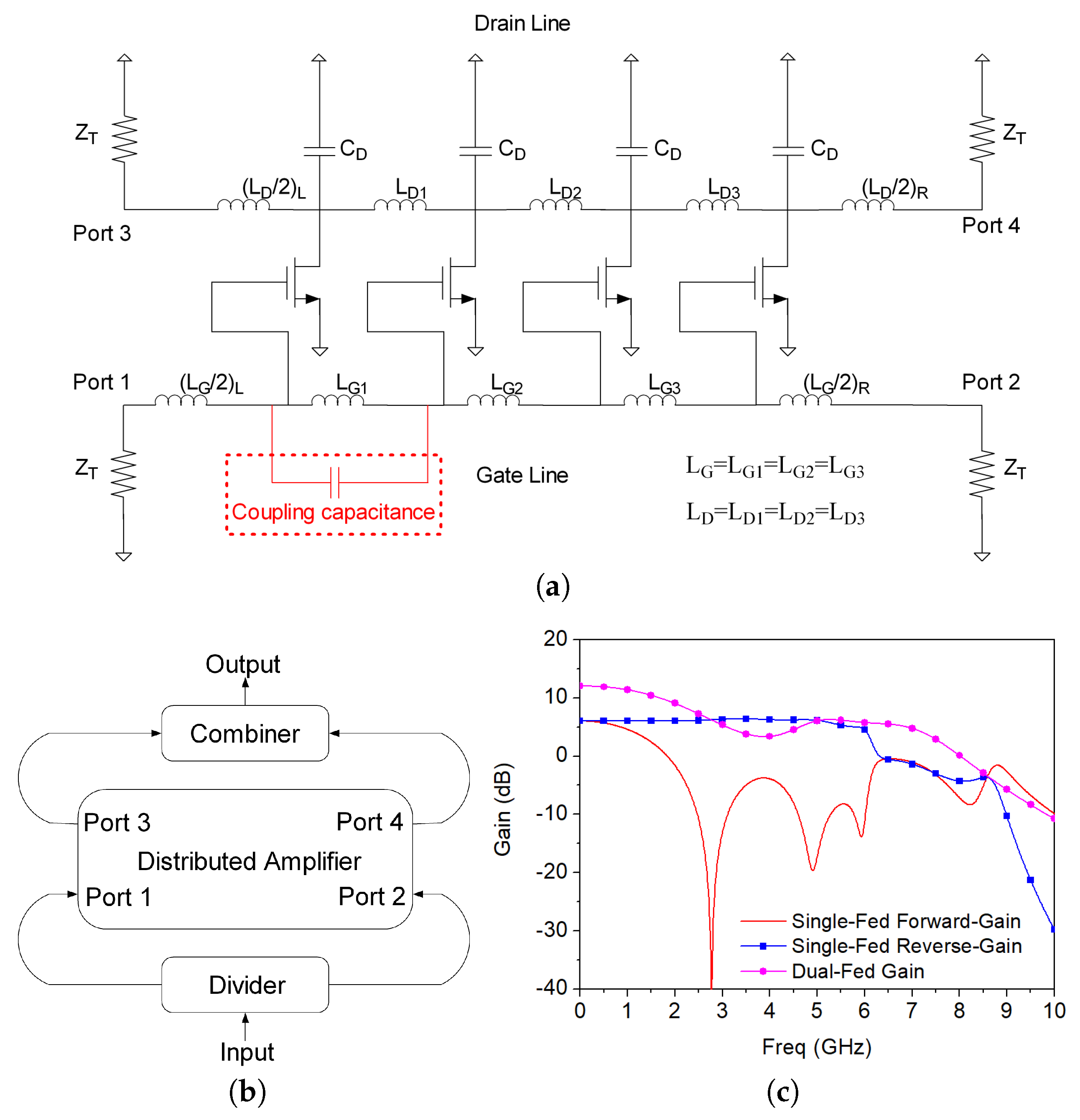
The circuit diagram of a conventional low-pass DA is shown in Figure 1a. In this topology, as the input signal flows through the gate transmission line, the output currents from each gain stage are added in the drain line. If the losses are not considered, the gain of a DA rises linearly as the number of stages is increased while the bandwidth stays constant. This is due to the fact that the parasitic capacitances of the transistors are assimilated into the gate and drain lines, forming lumped-element T-section constant-k filters, whose cut-off frequency limits the bandwidth of the circuit [1]. The characteristic impedance (Z0) and cut-off frequency (fc) of both transmission lines (TL) are given by:
Since Z0 and fc of both lines are identical, their capacitances and inductances should also be equal. As the drain-to-bulk capacitance (Cdb) of a Metal Oxide Semiconductor Field Effect Transistor (MOSFET) is typically lower than its gate-to-source capacitance (Cgs), a capacitor (Cd) is included at the drain so both capacitances are equivalent:
When losses are taken into account, the signal at each stage of the DA is attenuated. The main contributors to these losses are finite Q inductors and the drain-to-source resistance (rds) in the drain line. Under these conditions, the gain of the DA is typically described as follows:
in which Ad and Ag are the attenuation of the drain and gate lines, gm is the MOSFET transconductance and N is the total number of stages. In this equation, the following assumptions are considered:
- Unilateral MOSFET model (ignores Cgd),
- Image impedance matched terminations,
- Equal gate and drain phase velocities.
The optimum number of stages that maximises the gain is a function of gate and drain line attenuation. These attenuations are complex functions and depend on the specific MOSFET parameters, as well as on the operating and cut-off frequencies. As the signal travels along the gate line towards the termination, less signal is available for each MOSFET due to the attenuation and, as a consequence, the overall gain decreases resulting in an increased number of stages. The number of stages for this work is chosen as 4.
The required gm can be found from the low frequency gain of Equation (5) when the gain, number of stages and drain-line inductance and capacitance are known, as shown in Equation (6):
Hence, the transistor width-length ratio can be derived from:
where:
- W, transistor gate width,
- L, transistor gate length,
- n, electron mobility,
- Cox, gate oxide capacitance per unit area,
- VT, threshold voltage,
- Vgs, gate-source voltage.
Finally, the device length and width can be found by combining Equation (7) with the following expression:
Conventional DA designs feature gate and drain transmission lines with low-pass characteristics and equal electrical lengths (g() = d()). As a consequence, the forward gain adopts a wideband nature, in which the corner frequencies of the unit cells are the limiting factor. On the contrary, the reverse gain follows a low-pass behaviour, as seen in Figure 1c.
The dual-fed configuration shown in Figure 1b benefits from the forward and reverse gains of the DA, improving both power and gain when its performance is compared to the single-fed topology. This increase will only occur at low frequencies, since the reverse gain has low pass frequency response despite the fact that the forward gain has a broadband response. This can be seen in Figure 1c, where the small-signal gain of a dual-fed DA is plotted.
3. Area Reduction Techniques
One of the main drawbacks of distributed amplifiers is that they are formed by a noticeable amount of inductors that occupy most of the layout. Hence, it is paramount to analyse the influence of the coils and their placement on the circuit.
The most obvious method is to place the inductors closer together, which results in a more compact layout. However, this causes positive mutual coupling between the inductors when they are coiled in the same direction. Otherwise, the coupling would be negative [9]. To summarise, in DAs with inductors placed close together, it is crucial to properly orientate the inductors in order to reduce the chip area by minimising the effect of mutual coupling [10].
By using multilevel inductors instead of the conventional single-level or planar inductors, area minimization can also be accomplished [11,12,13,14,15] (see Figure 2a). In the multilevel structure, the coil is expanded vertically, while in the single level structure, the inductor is implemented using a single metal layer. Typically, the top layer is used to enhance the quality factor of the coil, since the lower metal layers are thinner. This means that, for a given inductance, the single-level structure shows a much larger area compared to a multilevel one. Using the thinner lower metal layers causes an increase of both the substrate capacitance and metal resistance. However, this disadvantage is compensated by the lower substrate losses due to their reduced area. This way, only a slight degradation of the performance of the stacked inductor is achieved compared to that of the planar spiral inductors.
Both methods show that it is possible to reduce the area without significantly modifying the small-signal circuit response [9]. However, a further reduction in area can be achieved if some inductors could be placed on top of others, as seen in Figure 2b, where they should be winded in the opposite direction in order to reduce the mutual inductance and capacitance that appears between them. Even though this method could minimise the area considerably, the increased capacitance between the inductors would lower the cut-off frequency of the artificial transmission lines, reducing the small-signal behaviour of the DA. This can be exploited to make a dual-fed distributed power amplifier due to its low-pass frequency response. The increased capacitance when two of the coils of the gate line (LG1 and LG2) are placed one on top of the other is shown highlighted in Figure 1a. Figure 3 shows a simulation of the forward and reverse gains when the coupling capacitance between both inductors is varied. As it can be seen, the frequency response of the forward gain is reduced, but the reverse gain remains the same. Therefore, if a dual-fed DA is made based on this topology, its gain will not be affected due to its low-pass frequency response.
4. Experimental Results
In this section, the suggested area reduction techniques will be corroborated. To do so, two four-stage DAs have been designed in a standard 0.35-μm CMOS technology using the component values shown in Table 1, which were obtained following the procedure explained in Section 2.
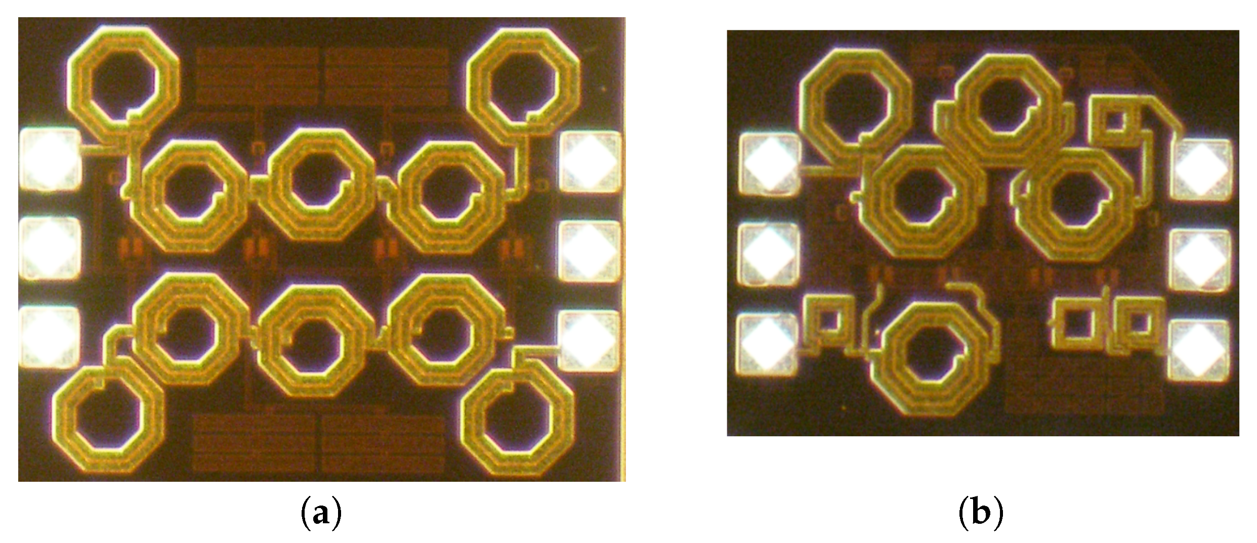
The fabricated circuits are shown in Figure 4, where DA1 and DA2 correspond to a conventional and a compact design, respectively. DA1 uses conventional spiral inductors without implementing any area reduction technique. The total area of this circuit is 0.742 mm2 including the pads. On the contrary, DA2 uses the area reduction techniques discussed in the previous section. First, a more compact layout has been obtained by placing the coils close to each other. To avoid the effect of the mutual coupling between the inductors, the coils have been oriented in the opposite direction. Additionally, multilevel inductors have been used on the gate line (LG3, (LG/2)R and (LG/2)L). Finally, two of the spiral inductors of the gate line (LG1 and LG2) have been placed one on top of the other (stacked) to share the same area. This circuit still uses conventional inductors in the drain line since the multilevel inductors cannot withstand the current going through this path. However, (LD/2)R has been implemented using a multilevel coil given that the current flowing through this inductor is lower since the circuit is biased using Port 3. By applying these modifications, the compact design occupies an area of 0.503 mm2, which results in a 32% area reduction.
Measurements were performed with on-wafer probing with two bias tees connected at the input and output ports. To implement the dual-fed versions, a power divider and combiner were included externally to the single-fed prototypes.
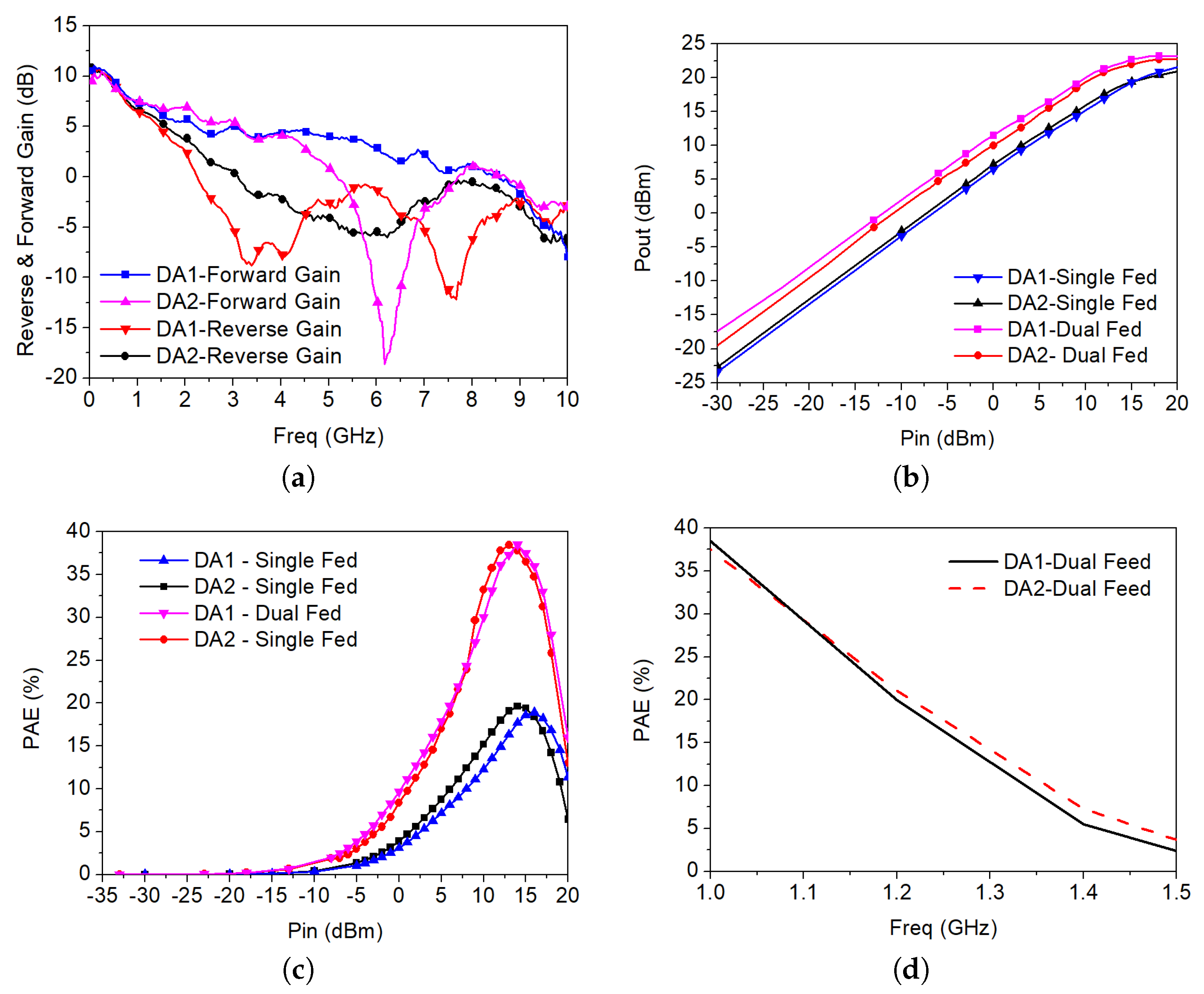
The measured forward and reverse small-signal gains are presented in Figure 5a. The experimental results were obtained using the same DC bias conditions: 3 V on the drains and 0.8 V on the gates. As expected, the forward gain of DA2 is reduced compared to that of DA1 due to the coupling capacitance between the inductors placed one above the other. However, the reverse gains are very similar.
The relation between the measured output power and the input power for both configurations at 1 GHz is shown in Figure 5b. Note that, to compare the performance, the input power level between the dual and the single-fed prototypes must be shifted 3 dB. As explained in Section 1, in the dual-fed configuration a 3 dB output power increment and a 6 dB gain boost is achieved when compared to the single-fed DA.
Figure 5c depicts the measured results of power-added efficiency (PAE) as a function of the input power at 1 GHz. The obtained values are close to the theoretical limit of 40%, which meet those obtained in previous works [8,16]. The PAE for the dual-fed configuration for a 14 dBm input power is shown in Figure 5d as a function of frequency. As expected, the low-pass frequency response of conventional DAs results in a PAE decrease as the frequency increases. Note that the bandwidth for both DAs is similar, provided that the frequency response of the dual-fed DA is limited by the reverse gain, which is similar for both circuits.
5. Conclusions
In this paper, several area reduction approaches have been implemented in a dual-fed DA. The first of them consists of placing the inductors closer together, considering that it is essential to properly orientate the coils in order to minimise the mutual coupling issue. The other techniques deal with the area occupied by the inductors, by using multilevel inductors and placing inductors one on top of the other.
The application of these techniques achieves a 32% area reduction, where the variation of the circuit performance is negligible. The large signal parameters, output power and PAE, remain practically the same. Even though there is a discrepancy between the small signal parameters of both versions, they are almost identical at the operating frequency, which is 1 GHz. It should be noted that the area of the circuit could be further minimised as the number of stages increases.
Author Contributions
J.d.P. and S.L.K. contributed to the design of both versions of the distributed amplifiers. All the authors contributed to the measurements and the writing process of the paper.
Funding
This research was funded by the Ministerio de Economía y Competitividad, Grant No. TEC2015-71072-C03-01 and by the Agencia Canaria de Investigación, Innovación y Sociedad de la Información Gobierno de Canarias, Grant No. ProID2017010067.
Conflicts of Interest
The authors declare no conflict of interest.
Abbreviations
The following abbreviations are used in this manuscript:
| CMOS | Complementary Metal Oxide Semiconductor |
| CRLH | Composite Right/Left-Handed |
| DA | Distributed Amplifier |
| DC | Direct Current |
| DPA | Distributed Power Amplifier |
| MOSFET | Metal Oxide Semiconductor Field Effect Transistor |
| PAE | Power-Added Efficiency |
References
- Wong, T.T.Y. Fundamentals of Distributed Amplification; Artech House: Boston, MA, USA, 1993. [Google Scholar]
- Campovecchio, M.; Le Bras, B.; Hilal, R.; Lajugie, M.; Obregon, J. Large Signal Design Method of Distributed Power Amplifiers Applied to a 2-18-GHz GaAs Chip Exhibiting High Power Density Performances. Int. J. RF Microw. Comput.-Aided Eng. 1996, 6, 259–269. [Google Scholar] [CrossRef]
- Duperrier, C.; Campovecchio, M.; Roussel, L.; Lajugie, M.; Quere, R. New design method of uniform and nonuniform distributed power amplifiers. IEEE Trans. Microw. Theory Tech. 2001, 49, 2494–2500. [Google Scholar] [CrossRef]
- Fang, K.; Levy, C.S.; Buckwalter, J.F. Supply-Scaling for Efficiency Enhancement in Distributed Power Amplifiers. IEEE J. Solid-State Circuits 2016, 51, 1994–2005. [Google Scholar] [CrossRef]
- Aitchison, C.S.; Bukhari, N.; Law, C.; Nazoa-Ruiz, N. The dual-fed distributed amplifier. In Proceedings of the 1988 IEEE MTT-S International Microwave Symposium, New York, NY, USA, 25–27 May 1988; Volume 2, pp. 911–914. [Google Scholar]
- D’Augustino, S.; Paoloni, C. Power Distributed Amplifier With Input-Output Combiners. IEEE Microw. Opt. Technol. Lett. 1994, 7, 312–315. [Google Scholar] [CrossRef]
- Vendelin, G.D.; Pavio, A.M.; Rohde, U.L. Microwave Circuit Design Using Linear and Nonlinear Techniques; John Wiley & Sons: Hoboken, NJ, USA, 1990. [Google Scholar]
- Ng-Molina, F.Y.; Martin-Guerrero, T.M.; Camacho-Penalosa, C. Power and gain considerations in distributed amplifiers based on composite right/left-handed transmission lines. IET Microw. Antennas Propag. 2010, 4, 1000–1006. [Google Scholar] [CrossRef]
- Del Pino, J.; Diaz, R.; Khemchandani, S.L. Area reduction techniques for full integrated distributed amplifier. AEU-Int. J. Electron. Commun. 2010, 64, 1055–1062. [Google Scholar] [CrossRef]
- Moez, K.K.; Elmasry, M.I. Area-efficient CMOS distributed amplifier using compact CMOS interconnects. IET Electron. Lett. 2006, 42, 970–971. [Google Scholar] [CrossRef]
- Goni, A.; del Pino, J.; Khemchandani, S.L.; Garcia, J.A.; Gonzalez, B.; Hernández, A. Study of stacked and miniature three-dimensional inductor performance for RFIC design. In Proceedings of the SPIE—The International Society for Optical Engineering’s–Microtechnologies for the New Millennium Design (VLSI Circuits and Systems Conference), Maspalomas, Gran Canaria, Spain, 2–4 May 2007. [Google Scholar]
- Goni, A.; del Pino, J.; Gonzalez, B.; Hernandez, A. An analytical model of electric substrate losses for planar spiral inductors on silicon. IEEE Trans. Electron Devices 2007, 54, 546–553. [Google Scholar] [CrossRef]
- Burghartz, J.N.; Jenkins, K.A.; Soyuer, M. Multilevel-spiral inductors using vlsi interconnect technology. IEEE Electron Devices Lett. 1996, 17, 428–430. [Google Scholar] [CrossRef]
- Geen, M.W.; Green, G.J.; Arnold, R.G.; Jenkins, J.A.; Jansen, R.H. Miniature multilayer spiral inductors for GaAs MMICs. In Proceedings of the 11th Annual Gallium Arsenide Integrated Circuit (GaAs IC) Symposium, San Diego, CA, USA, 22–25 October 1989; pp. 303–306. [Google Scholar]
- Aguilera, J.; Melendez, J.; Berenguer, R.; Sendra, J.R.; Hernandez, A.; del Pino, J. A novel geometry for circular series connected multilevel inductors for CMOS RF integrated circuits. IEEE Trans. Electron Devices 2002, 49, 1084–1086. [Google Scholar] [CrossRef]
- Eccleston, K.W. Compact dual-fed distributed power amplifier. IEEE Trans. Microw. Theory Tech. 2005, 53, 825–831. [Google Scholar] [CrossRef] [Green Version]
Figure 1.
(a) conventional DA; (b) dual-fed DA; (c) small signal gains.

Figure 2.
(a) multilevel inductor; (b) stacked inductor.
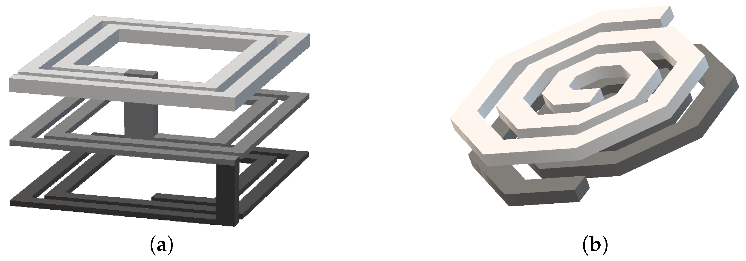
Figure 3.
(a) single-fed forward gain; (b) single-fed reverse gain and (c) dual-fed gain for different values of the coupling capacitor between LG1 and LG2 (from 0 to 0.7 pF).
Figure 3.
(a) single-fed forward gain; (b) single-fed reverse gain and (c) dual-fed gain for different values of the coupling capacitor between LG1 and LG2 (from 0 to 0.7 pF).
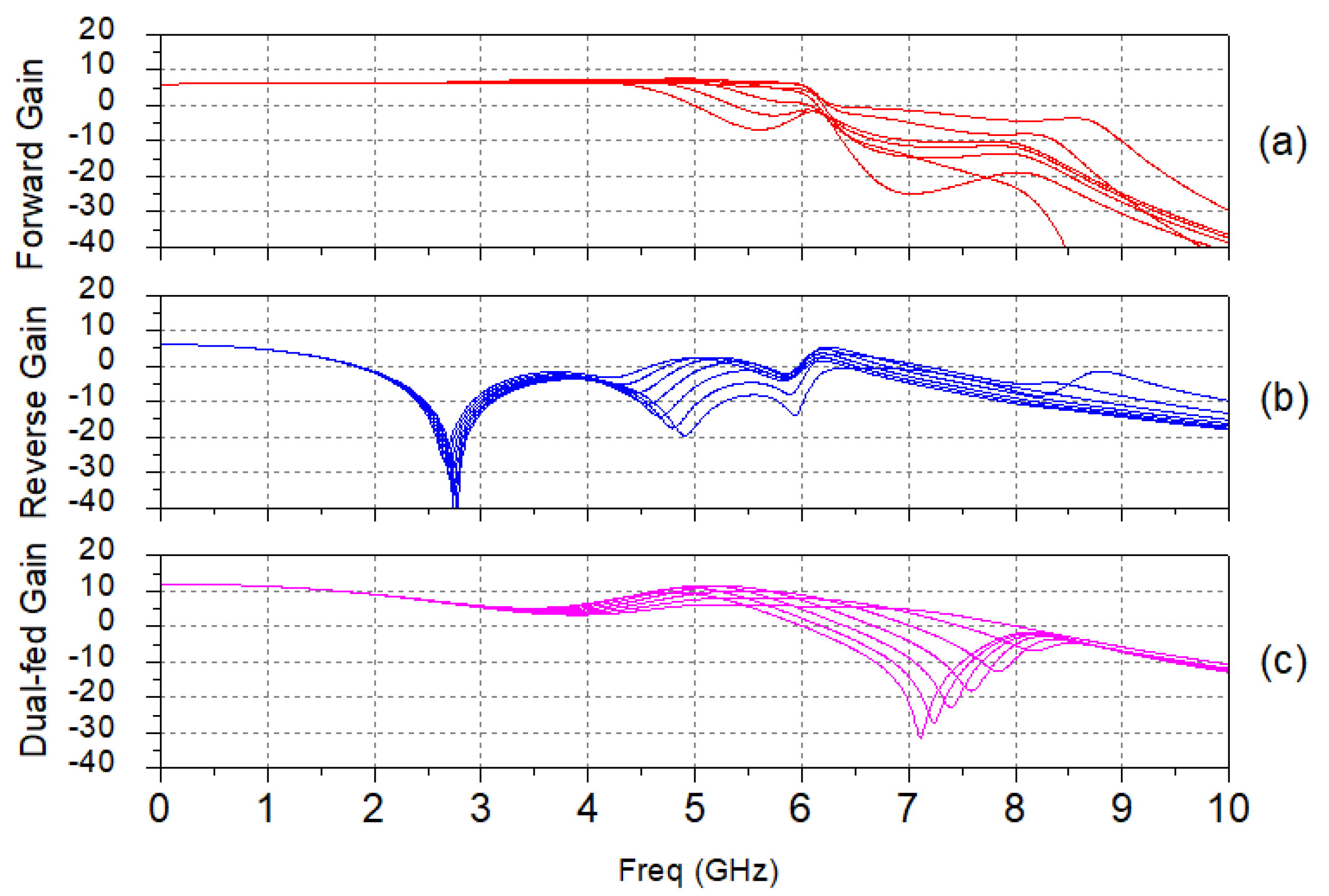
Figure 4.
Chip microphotograph of (a) DA1 (0.742 mm2) and (b) DA2 (0.503 mm2).

Figure 5.
Measured DPAs (a) s-parameters; (b) output power vs. input power at 1 GHz; (c) PAE vs. input power at 1 GHz; (d) PAE vs. frequency (Pin = 14 dBm).
Figure 5.
Measured DPAs (a) s-parameters; (b) output power vs. input power at 1 GHz; (c) PAE vs. input power at 1 GHz; (d) PAE vs. frequency (Pin = 14 dBm).


Table 1.
Component values.
| Component | Value |
|---|---|
| Lg = Ld | 1.465 nH |
| Cd | 586 fF |
| L | 0.425 μm |
| W | 4.42 μm |
© 2018 by the authors. Licensee MDPI, Basel, Switzerland. This article is an open access article distributed under the terms and conditions of the Creative Commons Attribution (CC BY) license (http://creativecommons.org/licenses/by/4.0/).
Share and Cite
MDPI and ACS Style
Pino, J.D.; Khemchandani, S.L.; Mateos-Angulo, S.; Mayor-Duarte, D.; San-Miguel-Montesdeoca, M. Area Efficient Dual-Fed CMOS Distributed Power Amplifier. Electronics 2018, 7, 139. https://doi.org/10.3390/electronics7080139
AMA Style
Pino JD, Khemchandani SL, Mateos-Angulo S, Mayor-Duarte D, San-Miguel-Montesdeoca M. Area Efficient Dual-Fed CMOS Distributed Power Amplifier. Electronics. 2018; 7(8):139. https://doi.org/10.3390/electronics7080139
Chicago/Turabian StylePino, Javier Del, Sunil L. Khemchandani, Sergio Mateos-Angulo, Daniel Mayor-Duarte, and Mario San-Miguel-Montesdeoca. 2018. "Area Efficient Dual-Fed CMOS Distributed Power Amplifier" Electronics 7, no. 8: 139. https://doi.org/10.3390/electronics7080139
Note that from the first issue of 2016, this journal uses article numbers instead of page numbers. See further details here.