1. Introduction
Efficient power supplies with fast transient response and accurate voltage regulation for low-voltage applications are becoming more important in today’s market. This can be mainly attributed to the fast growth and increase in demand for data-centers, as well as the massive increase in the amount of data being transmitted. It is estimated that the amount of annual global data-center traffic will increase from 4.7 zettabytes in 2015 to 15.3 zettabytes in 2020, where 1 ZB = 2
40 gigabytes [
1]. Also, the user base of consumer cloud storage is predicted to increase from 47 in 2015 to 59% in 2020 [
1]. With the current system design of data-centers, there is a significant volume of these low-voltage power devices in use when it comes to voltage regulation [
2]. As a result, it is critical to optimize the design of these power devices such that high efficiency and performance are achieved in data-center power regulators.
The laterally double-diffused metal oxide semiconductor (LDMOS) transistor offers higher levels of integration for integrated circuits (ICs) [
3]. As a result, the LDMOS is viewed as a viable solution for advanced systems on a chip (SoC), which have power integrated within the solution combining both high speed digital logic CMOS and high power LDMOS devices onto the same silicon chip [
4]. These SoCs are often found in Internet of Things (IoT) applications. LDMOS devices have also found a footing in advanced integrated power electronics modules and electric vehicles that are now rampant in the market.
The work presented gives a viable solution for improving upon the design of 30 V power devices. The super-junction (SJ) technique, which involves the use of consecutive N and P pillars in the device’s drift region and is well established in the high voltage (600 V) range, is tested here for the low-voltage range. In [
5] the authors attempt to integrate the SJ technique within their low-voltage device design, but from [
6,
7], and further investigation here, it can be seen that the SJ technique may not be preferred for low-voltage applications. An alternative approach to designing a 30 V power device is proposed by replacing the SJ pillars and the shallow trench isolation (STI) with a floating p-type layer in the drift region.
This paper contains five sections. Following the introduction,
Section 2 discusses the low-voltage Super-Junction LDMOS that was investigated in this work.
Section 3 covers all of the details for the floating P layer device and explains how it can be used to replace SJ devices at low-voltages (30 V range).
Section 4 presents a new concept of combing both STI technology with a floating P layer to generate a device with a very low figure of merit (FOM) (
QG ×
RDS(on)).
Section 5 gives a summary.
2. Low-voltage SJ LDMOS Analysis
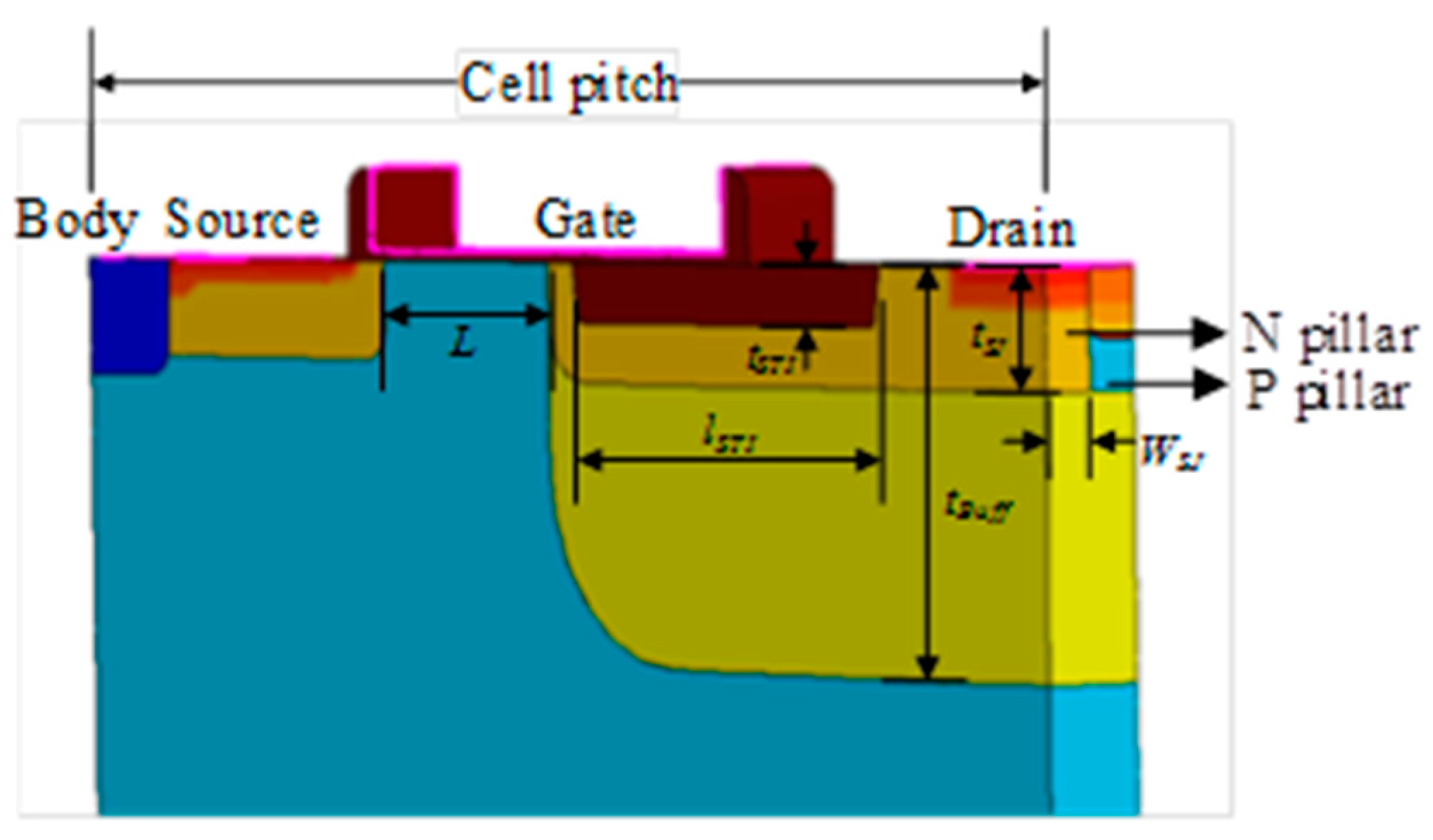
Figure 1 shows a conventional LDMOS used in our simulation, while the structure of the SJ LDMOS device is displayed in
Figure 2. The SJ LDMOS in
Figure 2 contains N and P SJ pillars. Shallow trench isolation (STI) is used in the drift region. This assists in absorbing the peak electric field that commonly occurs at the edge of the gate [
8]. Both the conventional and SJ devices are simulated using two-dimensional (2D) and three-dimensional (3D) Sentaurus Device TCAD. For the conventional device, it was possible to simulate it in a 2D environment, while the SJ LDMOS is simulated in 3D. The SJ LDMOS is quite unique in that the SJ N and P pillars do not exist on the front facing 2D cross section, but the pillar array is placed within the width of the device, requiring a 3D simulation [
9].
Table 1 lists the super-junction LDMOS key device dimensions.
The device simulation uses the following physics models: Old Slotboom model [
10] for the effective intrinsic carrier density; while doping dependence [
11], high field saturation [
12], and Lombardi [
13] models are used for the mobility dependence. Shockley Reed Hall [
14], Auger [
15], and Okuto avalanche models [
16] for the recombination and breakdown current.
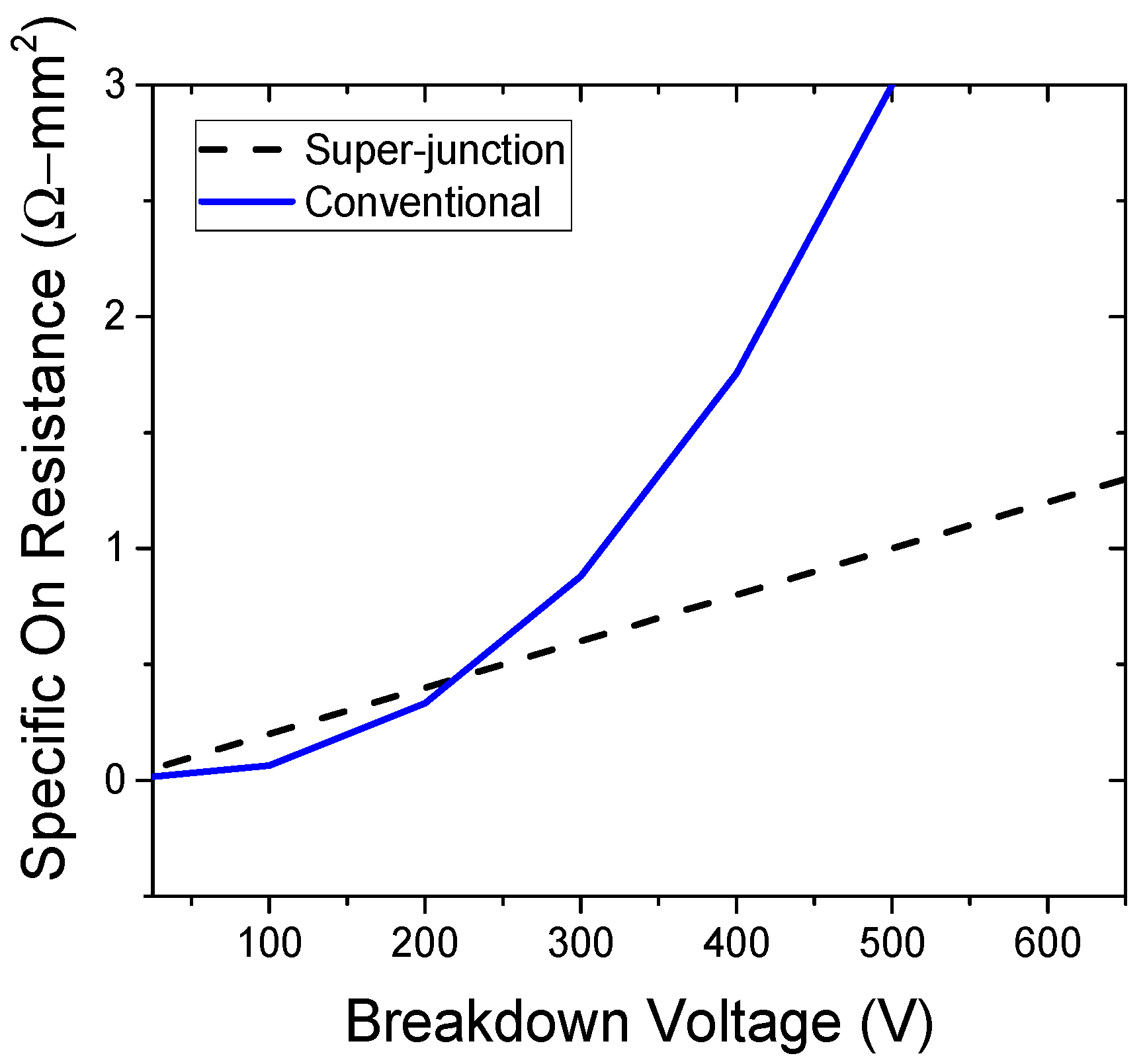
Figure 3 compares the on-state resistance (
RDS(on)) and gate charge (
QG) between the conventional device and the SJ device. Both devices have a breakdown voltage of 30 V. The conventional device has a FOM of 123 mΩ-nC while the SJ device has a FOM of 51 mΩ-nC. Note that
RDS(on) and
QG are both normalized to an active area of 1 mm
2.
RDS(on) was examined at the 1 A device operating point in the linear region.
QG was extracted from the gate voltage (
VGS) versus
QG plot in Sentaurus.
From
Table 2 we can see that at the same operating voltage of 30 V, the low-voltage SJ has a slight increase in
RDS(on), but a lesser amount of charge is accumulated at the gate terminal. This leads the SJ device to have an overall improved FOM, lower than that of the conventional device. It is worth pointing out that lower
QG leads to improved switching losses, while lower
RDS(on) helps reduce conduction losses. Conduction losses are significant in switching power supplies at low frequency [
17]. The conduction losses become an even more critical factor when looking at most modern soft switching topologies. Soft switching topologies significantly reduce the switching losses by switching at either zero current or zero voltage [
18].
The lack of improvement in
RDS(on) of the examined SJ LDMOS device reduces or negates the benefit of using SJ for the 30 V range. Equation (1) shows the on-state resistance as a function of breakdown voltage (
BVDss) for both the conventional and SJ devices [
6]:
where
BVDss is the breakdown voltage,
a is a constant that discerns between low-voltage and high voltage devices (
a = 6.21 for a 30 V conventional device &
a = 1.87 for a 600 V conventional device, and
a = 6.9 for a 30 V SJ device &
a = 2.07 for a 600 V SJ device),
B is the radiative recombination constant,
µn is the electron mobility,
ε is the silicon permittivity,
ND is the drift doping, and
A is the active area.
Equation (1) is often used to derive the silicon limit line (
RDS(on)× active area). In capturing
RDS(on) in Equation (1) as a function of
BVDss, the analytical equation uses the constant
a, whose value changes depending on the breakdown voltage of the device. This difference stems from the design of the device and the growth of drift region length as the device size gets larger for higher breakdown voltages. It is worth pointing out that the
RDS(on) model presented in Equation (1) is based on a dominant drift resistance. As the size of the device and drift length decrease, the ratio over which the drift resistance contributes to the overall resistance also decreases. For example, for a 600 V device the drift resistance is 96.5% of the total resistance [
6]. However, for a 30 V device, the drift resistance is only 29% of the overall on-state resistance.
Figure 3 gives a plot of simulated results using Equation (1) comparing the
BVDss versus
RDS(on) trend for both the super-junction device and the conventional device. From
Figure 3 it is evident that for devices with
BVDss less than 200 V the conventional device achieves a lower
RDS(on) than that of SJ, but this trend is reversed for devices with
BVDss greater than 200 V. For this reason, and also from our obtained simulation results, it is evident that the use of SJ technique to design power devices is more suitable to design high voltage power devices [
19] than low-voltage ones. The off-state breakdown voltage and on-resistance can be expressed by the analytical equations below:
where
Ecrit is the critical breakdown electric field for silicon,
EL = SJ pillars lateral electric field value,
tSJ is the SJ pillar depth,
Wn is the SJ pillar width.
The SJ technique also comes with some process complexities. These arise from the meticulous need to accurately balance the implantation charge required to realize the N and P pillars in the fabrication process. Any implantation imbalance between the pillars leads to a significant reduction in the device’s breakdown voltage [
7]. Another issue stems from the scaling of these SJ pillars for low-voltage applications: Equations (2) and (3) list the
BVDss and
RDS(on) dependence on the depth and width of the SJ pillars [
20]. Most modern SJ manufacturing, such as in [
21], rely on ion implantation. However, the need to scale down the SJ pillars while at the same time still ensuring their optimal performance may make their fabrication process too challenging and costly, due to the ion scattering that becomes more problematic when features are small.
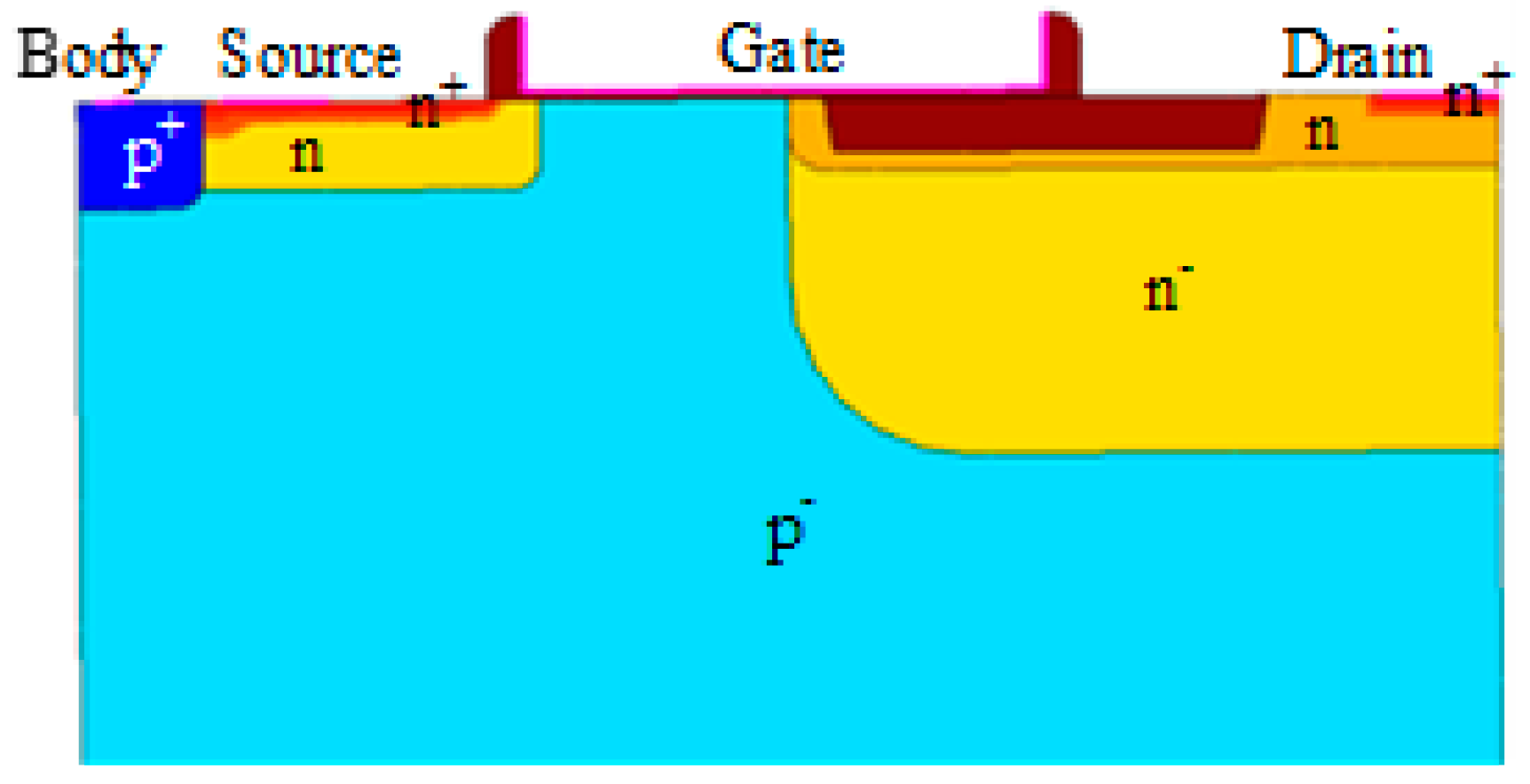
3. LDMOS with Floating P-Type Layer
The implementation of a floating p-type layer in place of the STI gate edge region is a technique that is examined for the LDMOS device; the method is also implemented in [
22]. The technique was investigated for low-voltage devices to measure the possibility to outperform SJ in this voltage range.
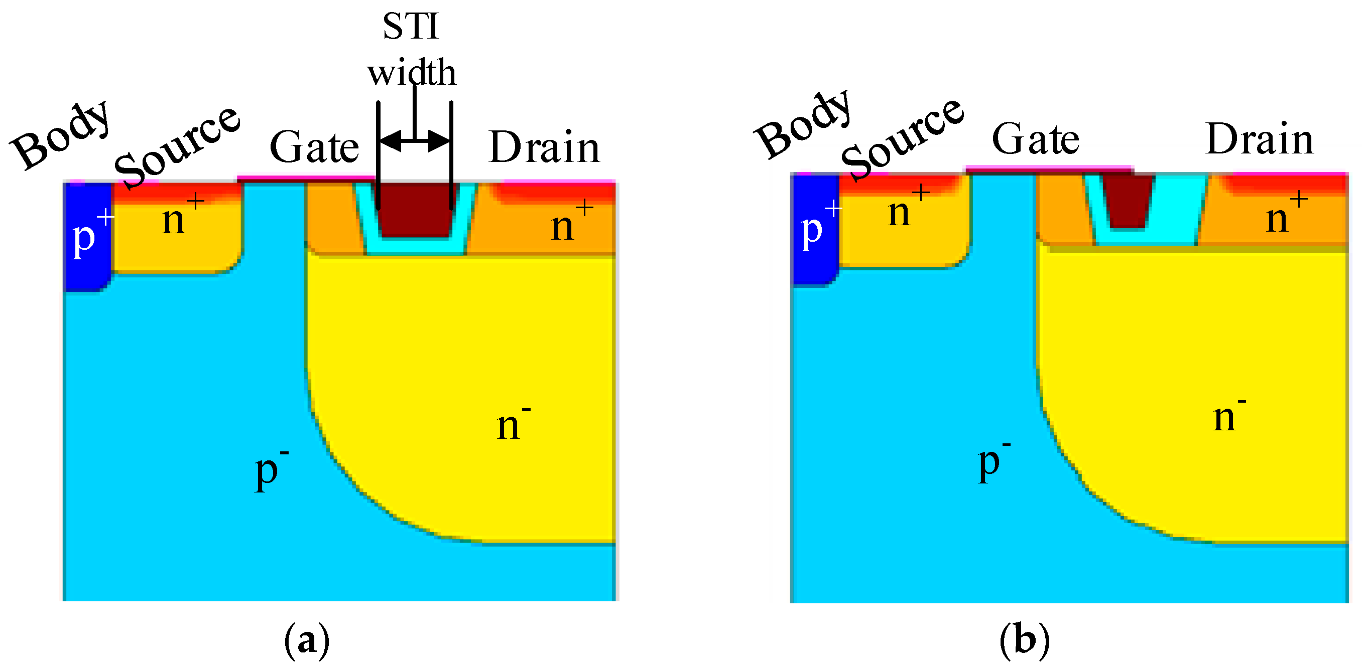
Figure 4 shows a cross section of the device considered. It can be seen from
Figure 5 that the device has a simpler 2D cross section when compared to that of the SJ LDMOS. Its device dimensions are given in
Table 3. The device cell pitch has also been modified and reduced from 8 µm to 3 µm. This achieves a higher cell density improving the on-state characteristics of the device.
Table 2 lists some of the key device dimensions.
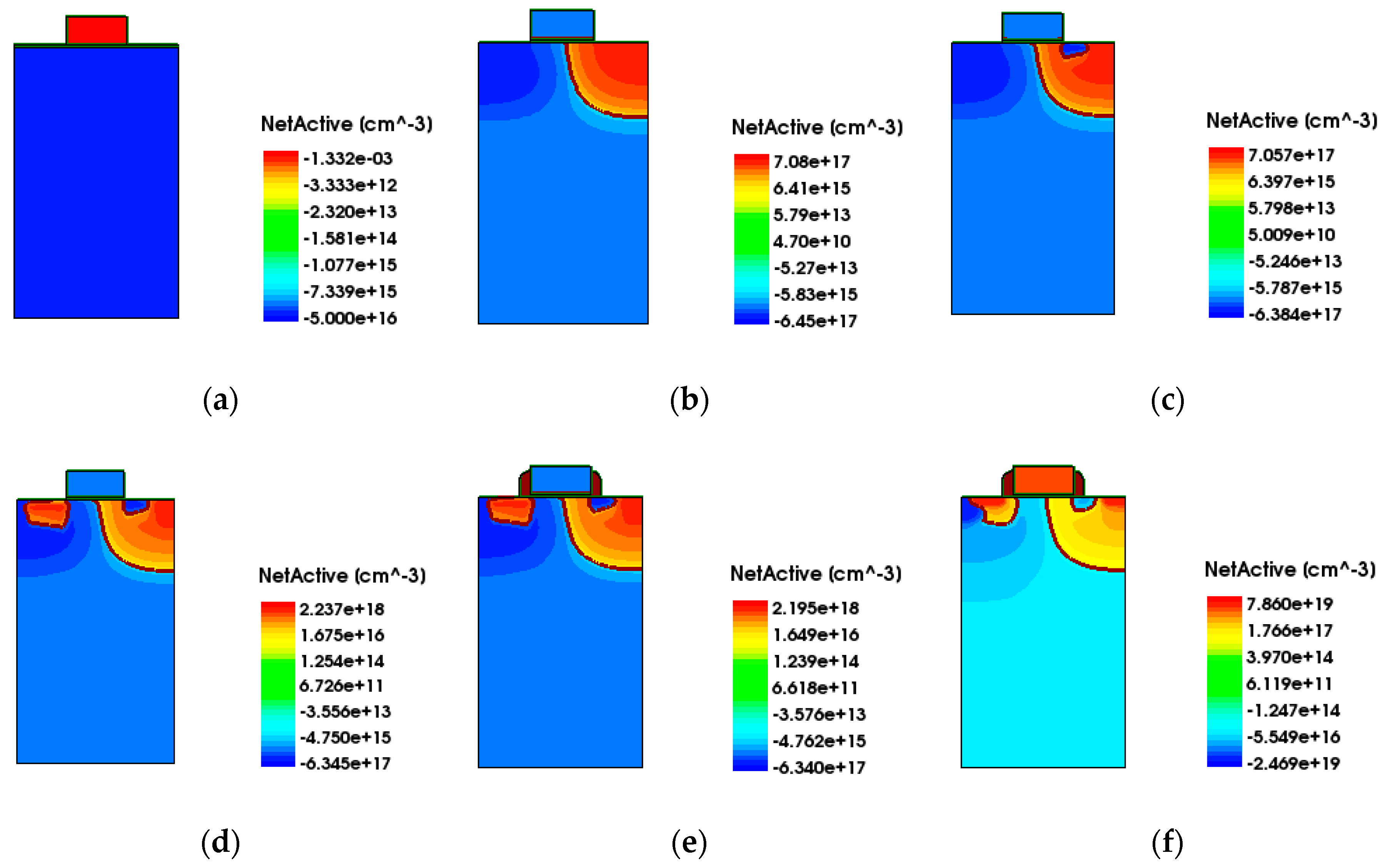
A process simulation for the p-type layer device was developed. The process simulation sheds light on how the added device features can be incorporated with relative ease, especially when compared to the complex SJ process.
Figure 4 shows cross sections of the device throughout the process.
The device is built on a <100> lattice p-type silicon wafer. The process is self-aligned to the gate: as such, the gate dielectric and the gate poly are initially deposited and patterned on the surface of the silicon wafer using the same mask. The P and N wells are then formed using the same mask with a combination of positive and negative photoresist, such that each dopant is deposited on either side of the gate. A dose of 3 × 1013 cm−2 with an energy of 150 keV is used for the N well, while a dose of 4 × 1013 cm−2 with an energy of 100 keV is used for the P well. The junction depth of the N well is around 1.35 µm, while the junction depth of the P well is around 1.40 µm.
For the floating p-type structure, implanting the dopants just under the edge of the gate on the drain side proved challenging, due to the fact that the process is self-aligned to the gate and the thickness of the polysilicon does not permit to implant the dopants directly. To solve this, an angled implant at varying energies was used to achieve the desired structure just under the gate edge. Four different doses of 3.5 × 1012 cm2 were used to obtain the desired profile; the energies used are in the following order: 20, 40, 80, and 160 keV.
The process is completed by implanting the phosphorus dopants for the source; a dose of 4.5 × 1013 cm2 is used with an energy of 70 keV. The dopants were activated using rapid thermal annealing (RTA) for 5 mins to stay within the thermal budget. Similarly the P+ body dopants were introduced as well as the N+ contact dopants, RTA is also used here to activate the dopants.
This floating P LDMOS process displays the feasibility and replicability of making the floating P device. The process advantage coupled with the performance improvement achieved with further optimization shows how the floating P layer device can outperform SJ devices at the 30 V application.
Table 4 gives a comparison of the
RDS(on) and
QG between the SJ device and the floating p-type layer device. Both devices have a breakdown voltage of 30 V. The FOM of both devices can be determined. The SJ device has a FOM of 51 mΩ-nC while the floating P layer device has a FOM of 9.75 mΩ-nC. Note that both
RDS(on) and
QG are both normalized to an active area of 1 mm
2. The performance enhancement seen in
Table 4 stems from the cell pitch optimization that was given to the floating P device. This led for the device unit cell to occupy less area resulting in an improved normalized
RDS(on) and
QG values.
4. LDMOS with STI Region Surrounded by P-Type Layer
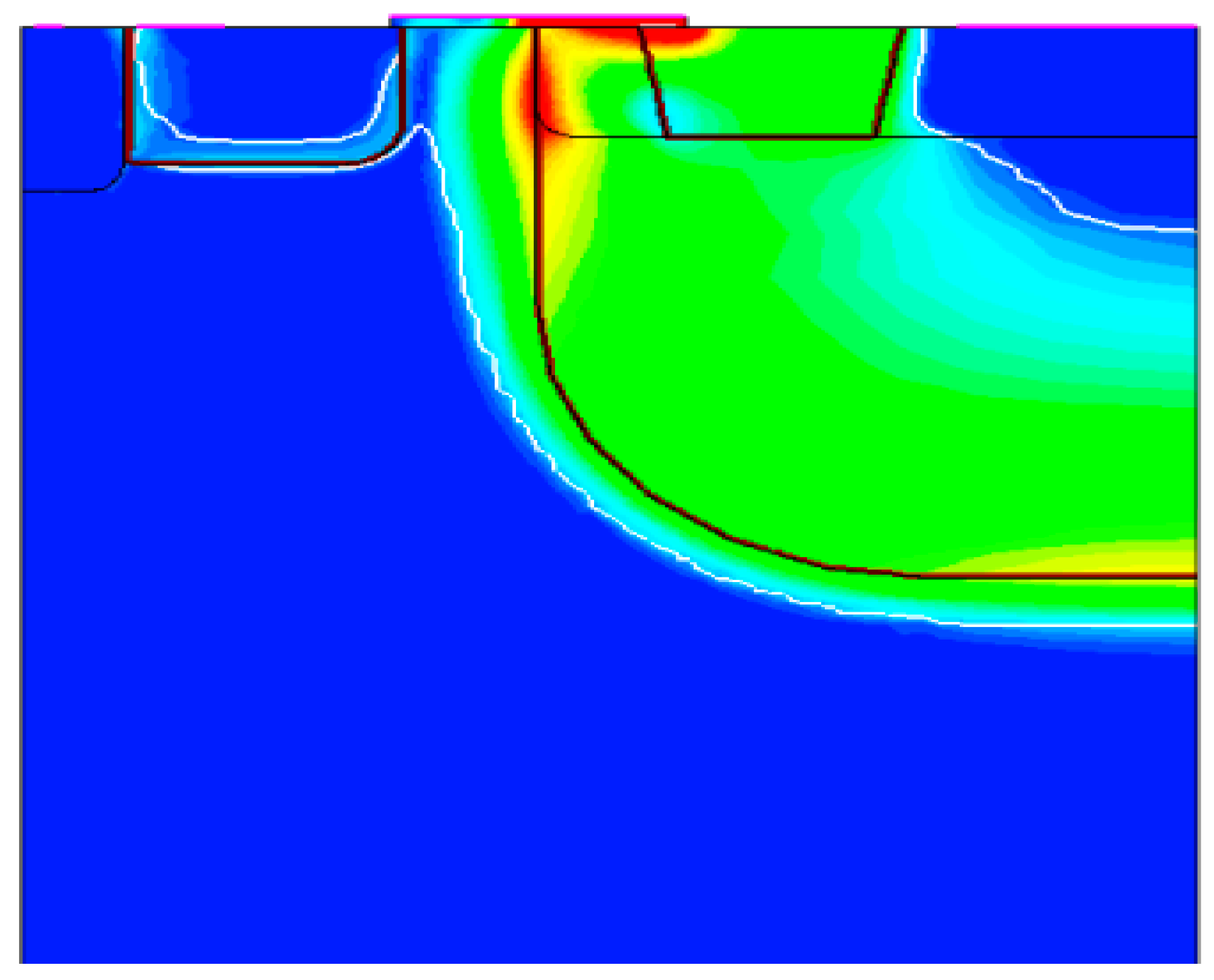
It was observed that the peak electric field of the floating P LDMOS device occurred on the surface of the p-type layer as shown in
Figure 6. It is known that the critical electric field of silicon is around 5 × 10
5 V/cm; the electric field on the surface exceeds that of the critical electric field as the device approaches breakdown and is the major source of impact ionization in the device. To counter the effects of the surface peak electric field, it was necessary to replace the material of the affected region with a material that has a higher critical electric field. Since the affected region is on the surface of the device, it is feasible with an SiO
2-filled trench realized at the same time and in the same way with the STI used in the fabrication process, as demonstrated in
Figure 7.
Table 5 gives the performance of the LDMOS device when the STI surrounded floating P layer technique is applied. Both devices are designed with a breakdown voltage of 30 V. The simulation results show that the device with the floating P layer has a FOM of 9.75 mΩ-nC while the device with STI plus floating P layer has a FOM of 5.93 mΩ-nC. That is a 39% improvement in the FOM. From our understanding of the current state of art, the implementation of such floating P layer with a STI region is a new design that led towards the given low FOM value observed by device simulation.
From
Table 5 one can notice that there is a slight increase in the gate charge of the STI plus floating P device which can be attributed to the wider surface area of the oxide in contact with silicon attracting a higher total number of charges. Despite this slight increase in
QG, the on-state resistance was reduced by a significant amount. The increase in
QG is due to the larger MOS capacitor plate area at the gate terminal caused by the addition of the STI region. The reduction in
RDS(on) stems primarily from the decrease of the depth of the p-type layer, as some of it is occupied by STI, leading to a thinner space charge region to be formed in the in the N
- buffer layer, which is in contact with the P layer. Since the buffer layer is lowly doped, any changes in the P layer dimensions would lead to sizable variation in the depletion width. The smaller space charge region causes a reduction in the device sheet resistance which leads to the lower on-state resistance.
The performance of the device was optimized by adjusting the size and placement of the oxide STI region.
Figure 8 plots the performance of the device when the STI is staggered by shifting it to the left. An STI width of around 0.25 µm was the optimal design point giving the desired 30 V breakdown and the
RDS(on) value is equal to 22.8 mΩ-mm
2. Reducing the STI width from 0.25 µm to smaller values will increase the on-resistance and decrease the off-state breakdown voltage, as shown in
Figure 8. For example, when the STI width is reduced from 0.25 µm to 0.125 µm, the
RDS(on) increases from 23 to 23.3 mΩ-mm
2 and the breakdown voltage decreases from 30 to 29 V. On the other hand, when the STI width is increased from 0.25 µm to 0.375 µm, the
RDS(on) decreases to 22.7 mΩ-mm
2 but the breakdown voltage decreases 29 V.
Figure 9 plots the performance when the STI is centered with respect to the mid-point of the P type layer. In this case, the optimal width for the STI centered with respect to floating P type region is around 0.28 µm. Similarly, reducing the STI width from 0.28 µm to smaller values will increase the on-resistance and decrease the breakdown voltage (see
Figure 9). When the STI width is decreased from 0.28 µm to 0.125 µm, the
RDS(on) increases from 22.8 to 23.3 mΩ-mm
2 and the breakdown voltage drops to about 29 V. On the other hand, when the STI width is increased from 0.28 µm to 0.375 µm, the
RDS(on) decreases to 22.5 mΩ-mm
2 but the breakdown voltage decreases 29 V as well.
From
Figure 8 and
Figure 9 one can see that that the staggered STI achieves an overall better performance as far as the on-state resistance is concerned. Also, the staggered STI achieves a lower
QG compared to the centered STI. This is due to the smaller surface area of the oxide under the gate field plate.


