Abstract
Reusable design using IP cores requires of efficient methods for protecting the Intellectual Property of the designer and the corresponding license agreements. In this work, a new protection procedure establishing an activation protocol in a similar way to the activation process in the software world is presented. The procedure, named SEHAS (Secure Hardware Activation System) allows the distribution of cores in either Blocked (not functioning) or Demo (functioning with limited features) modes, while ensuring the license agreements by identifying not only the IP core but also the implementation device, using Physically Unclonable Functions (PUF). Moreover, SEHAS secures the exchange of information between the core and the core vendor using an Elliptic Curve Cryptosystem (ECC). This secure channel allows the IP core vendor to send a unique Activation Code to the core in order to switch it to the Activated Mode, thus enabling all its features.
1. Introduction
Reusable design has improved the costs and the human resources required for the development of complex systems. Nevertheless, the distribution of reusable modules in the form of Intellectual Property Cores (IP Cores) leads to new challenges for an adequate licensing and protection of the developer rights. In fact, once the IP Core has been delivered, the developer loses the control on how the core is used or redistributed. In the literature, several solutions for the protection of IP Cores at different description levels have been proposed [1,2,3,4,5,6,7,8,9,10,11,12,13,14], with watermarking techniques implemented at the HDL level the most suitable for IP core protection [2,3,4,5,6,7,8,9].
These methods allow the identification and ownership proof of the protected cores by means of a Digital Signature (DS), but they do not provide mechanisms for detecting unauthorized distribution of the a core since the physical device used for the implementation is not considered in the protection process. In this sense, Physical Unclonable Functions (PUF) [15,16,17,18,19,20,21] can provide a unique identification of the device, thus enabling the possibility of establishing a license for an IP core being implemented on a specific device. This can be achieved through the combination of the DS of the core with the Device ID (DID) provided by the PUF. In principle, the IP core vendor has access to the IP core information, and can thus embed a DS into the core under protection, but the vendor has no access to the device, which is held by the customer. Therefore, it is necessary to establish a secure channel for exchanging information between the device and the vendor in order to incorporate the DID information within the IP core under protection. The solution for establishing this secure channel can be the use of a Public Key Cryptosystem (PKC) [22,23] to be implemented into the IP core. This PKC implementation should require low area resources in order to minimize the area overhead introduced by the protection system.
Elliptic Curve Cryptography (ECC) [24] has emerged as the preferred solution for the hardware implementation of a PKC when low area, low power consumption or narrow bandwidths are required [25,26]. In fact, ECC requires lower key sizes than RSA for maintaining similar security levels [22,27], while allowing efficient hardware implementations when binary fields () are used [28,29]. Thus, the introduction of both PUF and ECC units into the IP core enables the identification of the core and the device, and allows the detection of license terms infringements also when the core is implemented on an unauthorized device. Moreover, it is possible to extend the features provided by the PUF and the PKC for enabling new features. Regarding this, the concept of Hardware Activation is introduced in [14] for the protection of microprocessor IP cores. The idea is similar to the activation process used in the protection of software programs: an activation code is required for allowing the system to operate properly, otherwise the system under protection remains inoperative or, optionally, in Demo mode. In this paper, taking advantage of the availability of a DS, a DID, and a secure channel for the interchange of information between the core and the vendor through the PKC, a generalization of the applicability of Hardware Activation to any type of IP core is proposed. The rest of the article is organized as follows: Section 2 describes the Secure Hardware Activation System (SEHAS), Section 3 presents the proposed designs and implementations for the different blocks composing SEHAS, and Section 4 is devoted to the conclusions of the work.
2. Secure Hardware Activation System
In the present work, a protection scheme enabling the Hardware Activation [14] of a protected IP core will be developed. The method, called SEHAS (SEcure Hardware Activation System), enables a detailed monitoring of license compliance through the generation of a unique Activation Code (AC) for each pair of IP core and implementation device. In this scheme, the IP core vendor can choose between two options for establishing the behavior of the core when the specific license Activation Code has been not supplied:
- Blocked mode. In this mode, the IP core remains blocked, without any functionality
- Demo mode. In this mode, the core maintains a limited functionality. This mode enables the possibility of distributing the core for performance and feature evaluation by the customer, in a similar way to the demo versions of software programs.
From any of these two states, the protected core is switched to Activated mode when the correct license AC is supplied, enabling all features of the IP core. Thus, the concept of Hardware Activation is similar to the activation process in the software world, but applied to the distribution and licensing of hardware IP cores. In the following subsection, the protocol for generating the Activation Code in a secure way is described.
2.1. Activation Protocol
The proposed protocol requires a set of operations to be performed by the customer and the IP core vendor. Figure 1 shows the flow diagram of the protocol, which comprises the following operations:
- Watermarking of the IP Core. The vendor generates a Digital Signature (DS), corresponding to the license details, and introduces it into the IP core to be protected by means of watermarking techniques such as IPP@HDL [6] or e-coreIPP [9].
- Introduction of the SEHAS module into the core. The logic needed for extracting the DS is included into the SEHAS module, which is after that embedded into the IP core. Note that the DS is not visible from outside at any time. Also, the structure of the IP core circuit, which includes the SEHAS module and the additional logic needed for protection, will not be modified later. Thus, if a Physical Unconlable Function (PUF) is used for obtaining the Device ID (DID), the PUF’s result will remain unchanged in the next steps. As a result of this operation, an IP core in Blocked/Demo mode is obtained and supplied to the customer.
- Generation of the Activation Request Code (ARC). The customer enables the generation of the ARC by introducing a given control sequence to the core. This ARC is the public key of the ECC PKC [22] established for securing the information exchange between the vendor and the core. The private key is obtained from the DS and the DID, thus including information about the IP core and the implementation device. Summarizing this all, the private-public key pair of the core are the CIC (Combined Identification Code, obtained concatenating the DS and the DID) and the ARC. Once the ARC is generated, it is sent to the vendor. In this way, the customer has no information about the DS or the DID, since only the public key (ARC) is sent.
- Generation of the Activation Code (AC) and the Secure Shared Value (SSV). The vendor generates its private-public key pair. The private key is named Core-Device License (CDL), and the public key is the Activation Code. Using the CDL (private key of the vendor), and the ARC (public key of the core), the Secure Shared Value (SSV) is computed. The same SSV can be derived from the CIC (private key of the core) and the AC (Public Key of the vendor).
- Generation of the ROM configuration. The SEHAS module contains a ROM, which includes part of the combinational logic of the protected core. Depending on the ROM contents, the core will be in Blocked, Demo or Activated mode. In this step, the vendor generates a ROM configuration that modifies the logic functionality of the core. This new ROM configuration enables the switch to the Activated mode by means of the SSV. Also, the vendor sends the AC to the customer. Again, the exchanged information is a public key, and the ROM configuration corresponds to modified logic functions without useful information. Moreover, the ROM contents could be encrypted if more security was needed, using a private-key cryptosystem. AES-128 can be implemented using only 444 LUTs [30], maintaining high levels of security with low area overhead. The private key to be used for ROM encription/decription will be the Digital Signature (DS) of the IP core.
- Activation of the protected core. The customer performs the ROM configuration, and supplies the AC to the core. The SEHAS module internally computes the SSV using the AC (public key of the vendor) and the CIC (private key of the core), then switching to the Activated Mode.
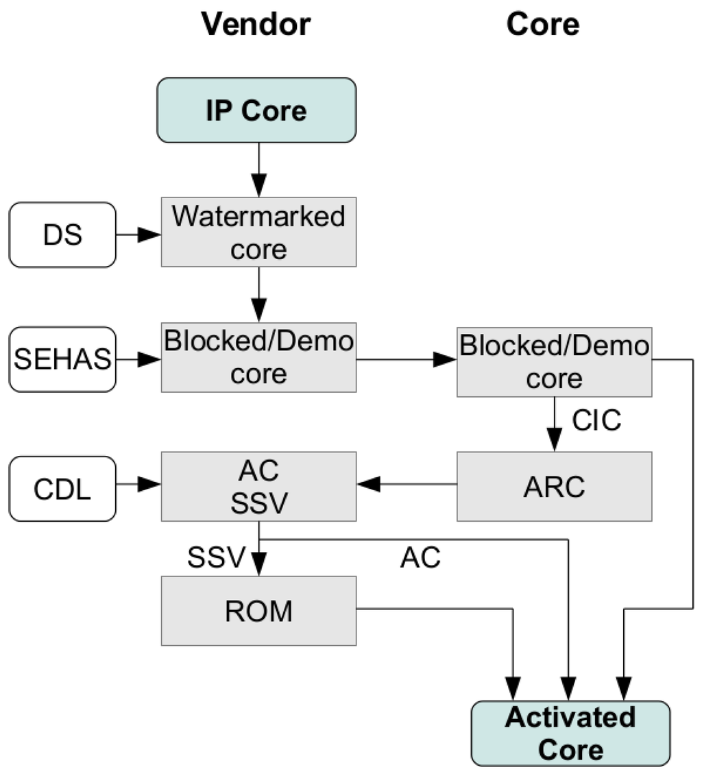
Figure 1.
Flow diagram for the hardware activation process.
As a result of the described process, the customer gets an activated IP core with full features. Note that this core will not correctly operate in a different device, because the CIC will be different (the DS will be the same, but the DID will not), and consequently the SSV obtained will not be able to switch the core to the Activated Mode. In the following subsection, the required elements for implementing SEHAS are described.
2.2. Hardware Structure for SEHAS Implementation
The activation protocol described above requires a set of hardware elements for implementing each of the operations. In Figure 2, the block diagram of an IP core protected using the SEHAS method is shown. The functions of the different blocks are the following:
- Watermarking Unit. Operation 1 of the activation process is performed through one of the watermarking techniques from those available in the literature [6,9]. As a result of applying such method, a DS will be stored in the protected core. The watermarking unit is the responsible for extracting the DS previously stored in the watermarked core, as it was detailed in Operation 2 above. The DS extracted will be concatenated with the DID generated by the Device Identification Unit, resulting in the CIC that is needed for completing Operation 3.
- Device Identification Unit. This unit provides the Device ID (DID), using a FPGA vendor specific function or a Physical Unclonable Function (PUF). In Section 3, these different possibilities will be considered. The DID obtained is combined with the DS supplied by the watermarking unit, generating the CIC.
- ECC Unit. The ECC unit performs the cryptographic operations needed by SEHAS. When the gen input takes the ‘0’ value, the ECC unit computes the ARC from the CIC and the base point G [22] (Operation 3). Note that activ input must take the value ‘1’ for obtaining the ARC at the output of the core. When gen input takes the ‘1’ value, ECC computes the SSV from the CIC and the AC, required for activating the core (Operation 6).
- SSV Register. The SSV register maintains the SSV value computed by the ECC unit, allowing the IP core to operate in Activated mode while powered on.
- AMC. The AMC block contains part of the combinational logic of the IP core under protection. The combinational functions are implemented using a ROM, with additional logic XOR-ing the functions with the SSV. Depending on the ROM configuration and the SSV, the core will be in Blocked, Demo or Activated mode.
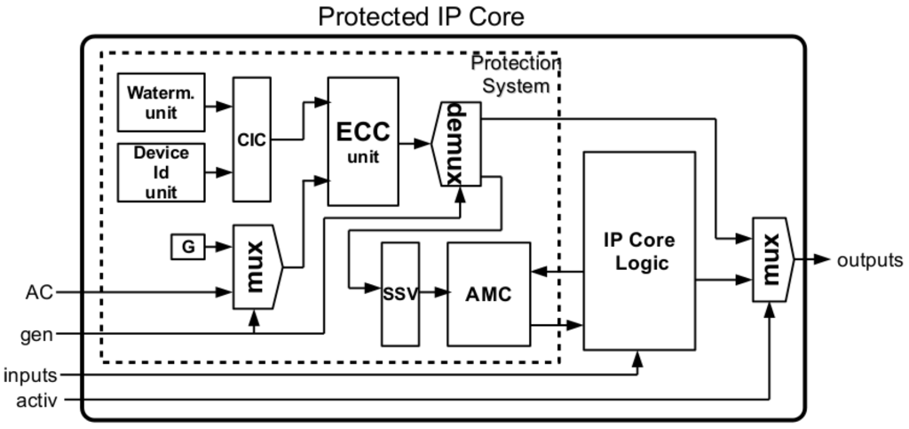
Figure 2.
Block diagram of a SEHAS protected IP core.
The next section proposes hardware implementations for the described modules.
3. SEHAS Blocks Implementations
In this Section, the implementation of each one of the SEHAS blocks is approached, considering different possibilities. The Watermarking Unit implementation depends on the technique used for storing the DS into the protected core. In [6,9], different watermarking techniques are described, along with the corresponding extraction logic. The next subsection approaches the implementation of the Device Identification Unit.
3.1. Device Identification in FPGAs Using PUFs
The usual target devices for reusable design using IP cores are Field Programmable Devices (FPLs), mainly FPGAs. The two main FPGA manufactures, Xilinx Inc. San Jose CA, USA, and Altera Corp. San Jose CA, USA, provide mechanisms for the identification of their devices. In the case of Xilinx devices, the families posterior to Spartan-6 contain an embedded, device-unique 57-bit identifier named “device DNA”, permanently programmed into the FPGA and unchangeable. The DNA information is stored in an eFUSE (Electrically programmable fuse) register, and can be read internally from the FPGA using the DNA_PORT primitive supplied by Xilinx. The DNA feature is not supported by all device families. Altera uses a similar technique, providing a 64-bit Altera Unique Chip ID, which can be recovered by means of the ALTCHIP_ID IP core. As in the case of Xilinx DNA, the ALTCHIP_ID is not available for all devices. Thus, using the unique DID provided by FPGA vendors makes the IP core technology dependent, and restricts the devices where it can be implemented. Physical Unclonable Functions (PUF) [15,16,18] represent an alternative capable of providing a DID based on process variations in the manufacturing of the device. The selected PUF must have two main properties:
- Variability. The PUF should generate a different DID for each device, and this DID must have good random statistical properties over different devices.
- Repeatability. The PUF should generate always the same DID in the same device, independently of the operating conditions.
There are different implementations proposed for PUFs on FPGAs [16,17,18,19,20], and in [21] an analysis of these proposals is outlined. From [21], implementations based on the different frequency generated by ring oscillators are more suitable to FPGAs than other solutions, such as arbiter PUF [20] or butterfly PUF [19]. In [18], a specific PUF for FPGAs is developed and presented, but it depends on the internal structure of the logic elements of the device. Here, we will use a PUF implementation based on the use of pairs of oscillators, whose frequency slightly differs as a consequence of process variations [17], as shown in Figure 3. Each oscillator feeds a counter, and the difference in the frequency causes a difference in the values presented by the counters at a given time. This difference is detected by a comparator, generating a bit which is stored in a latch or flip-flop (FF block).
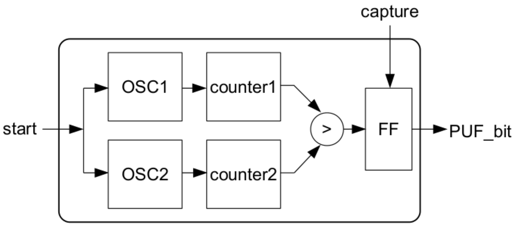
Figure 3.
PUF bit diagram.
The oscillators are usually implemented using Ring Oscillators (RO), as proposed in [16], allowing the control of the oscillator frequency by increasing or reducing the number of elements in the ring. In this paper, a new implementation of the oscillators is proposed, using a T flip-flop chain as a frequency divider for achieving a better waveform, while reducing the area of the counters. The length of the T flip-flop chain determines the stability of the clock signal obtained from the oscillator, and experimental tests realized using a logic analyser show that a chain with 4 flip-flops provides a stable waveform. Moreover, the oscillators have an start input for synchronizing the start time of both oscillators, and a capture signal for establishing the time when the counters are compared. The interval between these two time instants must be long enough to allow the counters to exhibit different values, which conditions the size of the counters. Generation of 960 PUF bits on 20 Altera DE-1 boards (Cyclone II EP2C20F484C7 devices) with 8-bit counters provides 502 ‘0’s and 458 ‘1’s. The difference between ‘0’s and ‘1’s occurrence is mainly due to the fact of having equal values in the counters results in a ‘0’ at the PUF output. Thus, 8-bit counters provide enough variability while maintaining a limited overhead.
On the other hand, repeatability has been tested performing 1000 repetitions of 48-bit NANDTO (NAND T-chain oscillator) PUF on each board. The experimental results provided a probability of obtaining an erroneous PUF output of . For improving repeatability, a majority function has been implemented, selecting the most repeated value in a three PUF calculation sequence. With this improvement, the probability of failing in the calculation of a 48-bit NANDTO PUF gets down to . Moreover, if 10 activation attempts are performed at boot time of the protected system, the probability of failing in the activation process is negligible.
For completing the PUF design, a control unit generates the start and the capture signals for synchronizing the start and end times of the PUF calculation. Figure 4 shows the proposed structure for the NANDTOs, and Table 1 shows the implementation results for 32-bit, 48-bit and 64-bit NANDTO PUFs over several devices from Altera and Xilinx. Implementations were performed using the following development boards:
- Xilinx Spartan-3AN Starter Kit (with xc3s700an-4fgg484 devices)
- Xilinx Spartan-6 SP605 Evaluation Platform (with xc6slx45t-3fgg484 devices)
- Xilinx Virtex-6 ML605 Evaluation Platform (with xc6vlx240t-1ff1156 devices)
- Altera DE-1 (with Cyclone II EP2C20F484C7 devices)
- Altera DE-2 (with Cyclone II EP2C35F672C6 devices)
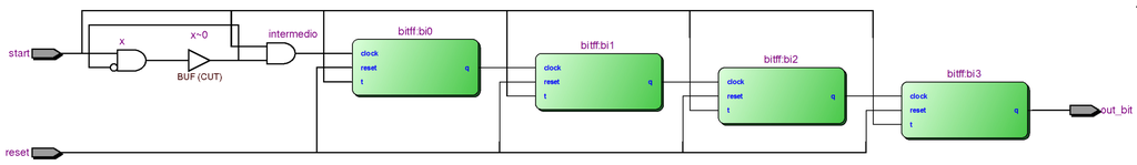
Figure 4.
NANDT Oscillator diagram.
The PUF generation requires 770 clock cycles, which is equivalent to 38.5 μs when operating at 50 MHz. The area required is not negligible because two counters (of at least 8 bits) along with the corresponding comparator must be implemented for obtaining each PUF bit.
With the NANDTO PUF presented, a DID for identifying the device when the manufacturer does not provide it is available. In the next section, the secure channel for interchanging information between the device and the vendor is detailed.

Table 1.
Area and delay figures for NANDTO PUF implementation on different devices.
| Device | # PUF Bits | # LUTs/LEs | Delay (ns) |
|---|---|---|---|
| Cyclone II EP2C20F484C7 (Altera) | 32 | 1241 (LEs) | 4.18 |
| 48 | 1849 (LEs) | 4.67 | |
| 64 | 2457 (LEs) | 4.98 | |
| Cyclone II EP2C35F672C6 (Altera) | 32 | 1241 (LEs) | 4.08 |
| 48 | 1849 (LEs) | 4.49 | |
| 64 | 2457 (LEs) | 4.89 | |
| Spartan 3AN xc3s700an-4fgg484 (Xilinx) | 32 | 897 (4-input LUTs) | 4.78 |
| 48 | 1329 (4-input LUTs) | 5.59 | |
| 64 | 1732 (4-input LUTs) | 5.66 | |
| Spartan 6 xc6slx45t-3fgg484 (Xilinx) | 32 | 732 (6-input LUTs) | 4.39 |
| 48 | 1084 (6-input LUTs) | 4.92 | |
| 64 | 1436 (6-input LUTs) | 5.26 | |
| Virtex 6 xc6vlx240t-1ff1156 (Xilinx) | 32 | 732 (6-input LUTs) | 2.83 |
| 48 | 1084 (6-input LUTs) | 2.85 | |
| 64 | 1436 (6-input LUTs) | 2.71 |
3.2. Low Area ECC Unit for Implementing a PKC in IP Cores
As pointed out in the Introduction Section, Elliptic Curve Cryptography (ECC) [22,24] is specially suitable for hardware implementation when fields are used. In the protection system described in this work, an ECC Unit will be included for ensuring communications between the device and the IP vendor. The next subsection introduces the background over ECC.
3.2.1. Elliptic Curves over Finite Fields
An elliptic curve E defined over a finite field consists of a set of points where and are elements of satisfying the Weirstrass equation [24], together with the point at infinite, O. In the [22] standard, the curves are defined by means of two coefficients and , named the coefficients of E. IF q is a power of 2, it must be in , and the points over E (except O) must satisfy the equation:
If , the field elements can be represented using polynomial bases, by choosing an irreducible polynomial . In this case, an element a of the field is represented using the bit string:
corresponding to the polynomial
where are elements of . When considering binary fields, the inverse of the point of the curve E is defined as:
One of the characteristics enabling the use of elliptic curves in cryptography is the possibility of defining an internal operation into the curve, named elliptic addition. Geometrically, the sum of two points P, Q is given by a point with the property that P, Q, and lie on the same straight line. From the full elliptic addition, the scalar product of a point P of the curve E and a natural n is defined as:
Moreover, given r a positive prime integer dividing the number of points on E, , and a curve point G of order r (generator of a subgroup of order r), an EC key pair can be defined. Specifically, taking as an EC private key, and as the associated EC public key, a public key cryptosystem for interchanging a secret value can be established. In fact, if two communicants A and B generate their corresponding EC key pairs , party A can compute the secret value using the public key of B. Then, B can recover the secret value from the public key of A, making because:
This is the basic principle for public key cryptography using EC, and the conditions to be met by the parameters involved and the details of the different primitives can be found in [22,24,31].
3.2.2. Domain Parameters for the ECC Unit
For the interchange of secure information between two counterparts, a set of domain parameters for the EC Cryptosystem must be established. The ECC unit must provide a secure communication channel with low area requirements, so we selected the finite field from the standard [23]. Using the curve B-163 from [32], the EC domain parameters used in the ECC Unit will be the following:
- (reduction polynomial for the field)
- (number of elements of the subgroup)
- (cofactor)
- (base point)
3.2.3. Scalar-Point Product Using the Montgomery Ladder Algorithm
As shown above, the scalar-point product is the basic operation for ECC, and it is the operation performed by the ECC Unit. There are several algorithms for the scalar-point multiplication, but the algorithm in [31] is the one preferred for EC cryptography. In fact, ML algorithm takes always the same number of steps, hindering side channel attacks, and the basic operation in each step is the field multiplication if projective or mixed coordinates are used [31]. Inversion (the most costly field operation) only is needed for coordinate conversion and the recovering of the y coordinate (the algorithm operates only over the x coordinate) [31]. Writing:
Algorithm 1 provides the scalar-point product . Note that the number of steps is fixed by m, being the number of steps independent of the k value, thus hindering side channel attacks based on analyzing power consumption.
| Algorithm 1: Algorithm 1 Montgomery ladder |
| Require: k, P |
| Ensure: |
|
|
|
|
|
|
|
|
|
The operations required in Algorithm 1 are point addition and doubling. When using projective coordinates, the operations in the main loop result in field multiplications, additions and squarings [31]. Addition and squarings are combinational operations, and inversion is only required for coordinate conversion, resulting in an execution time of [28]:
The execution time can be reduced if only Koblitz curves [32] are used [28]:
For the sake of generality, the ECC unit will support all types of standard curves, with the approximate execution time stated in Equation (8). In the implementation of the ECC Unit, performance is not critical because the PKC operations will be carried out only during the "boot" process. Thus, the design will be oriented to optimizing the area requirements.
The main field operations required for the scalar-point operation are multiplication and inversion. For field multiplication, the implementation in [33] allows completing the operation over requiring only 504 LUTs, and taking 163 clock cycles. Regarding inversion, although very efficient inversion implementations based on the Itoh-Tsujii algorithm [29] are available, the divider proposed in [34] needs only 836 LUTs on Xilinx devices [28]. Figure 5 shows the block diagram of the ECC Unit, and Table 2 presents the implementation results for the ECC scalar-point multiplication unit proposed.
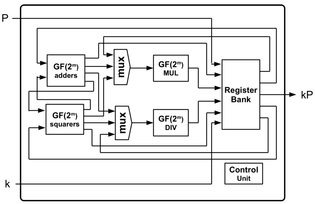
Figure 5.
ECC scalar-point unit diagram.
Table 2.
Area and delay figures for ECC unit implementation on different devices.
| Device | #LUTs/LEs | Delay (ns) |
|---|---|---|
| Cyclone II EP2C20F484C7 (Altera) | 6093 (LEs) | 10.53 |
| Cyclone II EP2C35F672C6 (Altera) | 6079 (LEs) | 9.06 |
| Spartan 3AN xc3s700an-4fgg484 (Xilinx) | 6525 (4-input LUTs) | 13.98 |
| Spartan 6 xc6slx45t-3fgg484 (Xilinx) | 4618 (6-input LUTs) | 7.95 |
| Virtex 6 xc6vlx240t-1ff1156 (Xilinx) | 4336 (6-input LUTs) | 5.12 |
The area required by the ECC Unit proposed is a bit higher than the design presented in [28] for Virtex 5 devices (4100 LUTs), but our design can operate with non-Koblitz curves such as B-163 [32]. Regarding performance, a scalar-point operation is completed in 8μs when operating at 50 MHz.
3.3. Activation Modes Circuit (AMC) Design
The third main block of the SEHAS protection system is the Activation Modes Circuit (AMD). This activation circuitry enables the different modes in the protected IP core, and performs the switching between modes as a function of a Secret Shared Value (SSV) generated from the AC. The AMC will include part of the combinational logic of the protected core, limiting the functionality of the core if the SSV is not valid. Figure 6 shows the structure of the AMC, which includes a ROM, a set of XOR gates, and a register containing the SSV. If , ... are the combinational functions to be implemented in the AMC, the function stored in the ROM is , where is the i-th bit of SSV. Thus, the only option for recovering the original functions is providing the correct SSV. The implementation of the combinational functions using a ROM presents two advantages:
- The vendor can provide the functions sending only the ROM configuration. This method does not produce any modification in the original circuit and, consequently, does not affect the PUF output.
- The vendor can provide functions for entering in Demo mode, if desired, without changing the structure of the circuit.
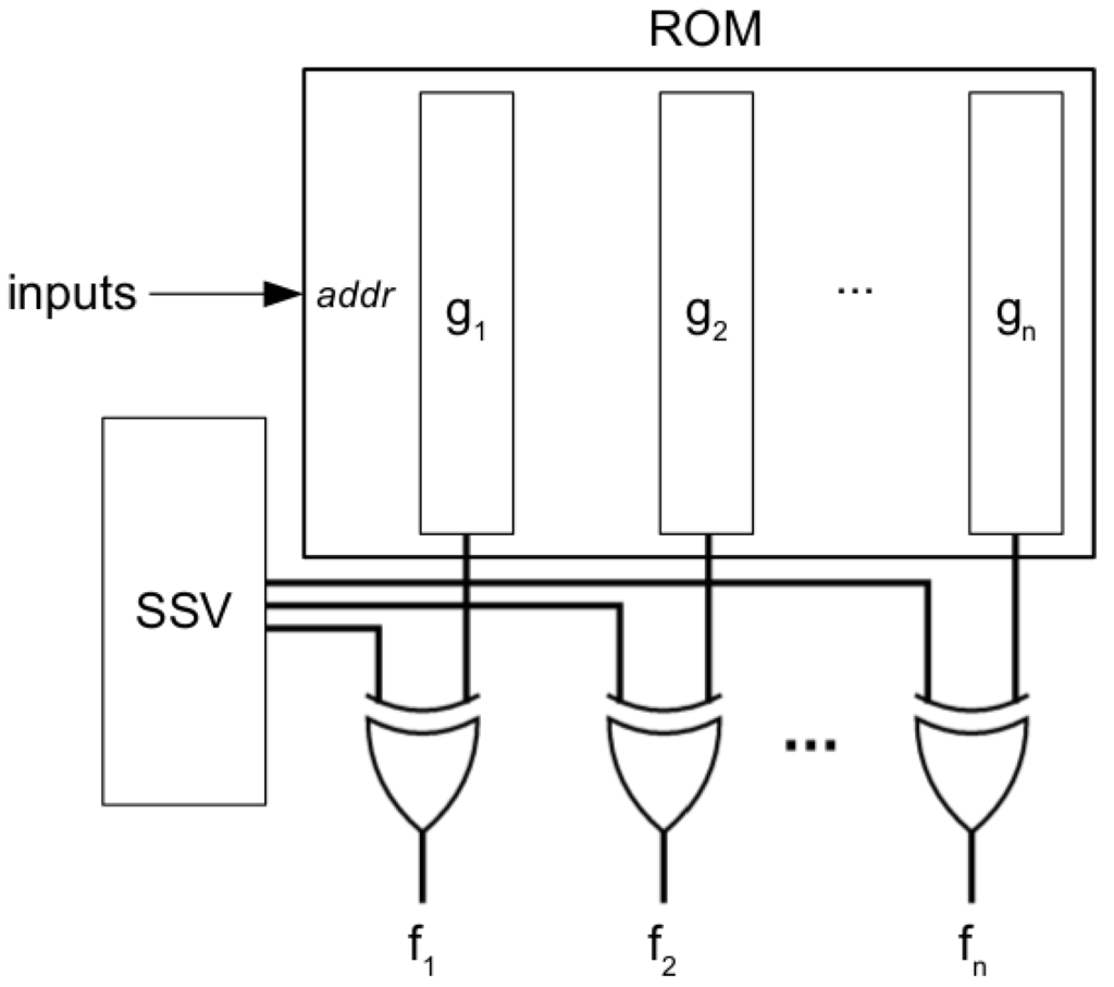
Figure 6.
AMC scheme.
If a finite field is used, the SSV will have m bits, and a maximum of m combinational functions can be included into the ROM. If the functions have n variables, the size of the memory will be . If , as stated in Section 3.2.2, and functions with are considered, a memory of 5216 bits is required. Although the current programmable devices have dedicated blocks of memory that can host this amount of memory without difficulty, not all designs contain this number of combinational functions. For maintaining the levels of security, the number of output bits must be maintained around , reducing the number of address bits of the ROM, and adding multiplexers at the output. As an example, if 10 functions of 5 variables are available, they can be included into a ROM with 1-bit address and 160 output bits, followed by 10 16-to-1 multiplexers. In the AMC, the multiplexers will be added at the output of the XOR gates. With these elements, the area of the AMC can be estimated as follows for accommodating k functions of n variables: will be the size of the k multiplexers at the output of the AMC. If , then the number of 6-input LUTs (Spartan 6 and Virtex 6 devices) required is given by:
Regarding the ROM memory, the number of address bits will be , and the ROM size:
Finally, the number of LUTs required for the XOR gates is , and the SSV register takes Thus, for the commented example with and , we will have h = 16, , , , , , and .
3.4. SEHAS Area and Performance Analysis
Previous sections have described the different blocks integrating SEHAS. Now, the complete SEHAS protection system will be analyzed, with special attention to the area and performance overhead. Because SEHAS allows different options, four designs will be considered:
- SEHAS-DID-ROM. In this design, the DID provided by the device manufacturers is used. Thus, DNA_PORT has been used for Xilinx devices, while ALTCHIP_ID was not available for the Altera devices used for tests. Regarding the AMC, a ROM with no encryption is used, resulting in the design with lowest area overhead.
- SEHAS-PUF48-ROM. This design assumes the unavailability of a DID supplied by the manufacturers, and makes use of a 48-bit NANDTO PUF. The AMC includes a ROM with no encryption.
- SEHAS-DID-AES. This design considers a SEHAS protection module taking advantage of DID functions provided by device manufacturers, and including an AMC with a ROM encrypted using AES-128.
- SEHAS-PUF48-AES. Finally, a design using a 48-bit PUF and AES encrypted ROM is considered.
Table 3 shows the results corresponding to these four designs. SEHAS-DID-ROM requires only 5200 LUTs for implementing the Hardware Activation protocol. This is affordable for medium-size cores, representing an area overhead of 5% on Ciclone IV (114,000 LEs) or 10% on Spartan-6 devices (55,000 LUTs). The total time required to complete an activation process, taking into account that SEHAS carries out 10 activation attempts before reporting a “failed activation”, is around 32.6 ms.
About power consumption, SEHAS requires around 800 mW at 50 MHz on Spartan-6 devices, but it operates only at boot time. Thus, SEHAS does not affect the power consumption of the IP core when it is in normal operation. It is difficult to compare SEHAS with other procedures, because it is the only protection method providing all the Hardware Activation features. There area other proposals, such as [35,36] using PUFs and symmetric encryption, but [35] uses a “simulated” PUF, and authentications are performed at FPGA configuration time. The proposal in [36] is based on integrating a PUF into the FPGA along with an AES module, thus being device dependent.
Table 3.
Area and delay figures for SEHAS implementation on different devices.
| Design | Device | #LUTs/LEs | Delay (ns) |
|---|---|---|---|
| SEHAS-DID-ROM | Cyclone II EP2C20F484C7 (Altera) | n/a | n/a |
| Cyclone II EP2C35F672C6 (Altera) | n/a | n/a | |
| Spartan 3AN xc3s700an-4fgg484 (Xilinx) | 7151 (4-input LUTs) | 14.98 | |
| Spartan 6 xc6slx45t-3fgg484 (Xilinx) | 5194 (6-input LUTs) | 8.15 | |
| Virtex 6 xc6vlx240t-1ff1156 (Xilinx) | 4934 (6-input LUTs) | 5.52 | |
| SEHAS-PUF48-ROM | Cyclone II EP2C20F484C7 (Altera) | 10251 (LEs) | 12.33 |
| Cyclone II EP2C35F672C6 (Altera) | 10249 (LEs) | 11.26 | |
| Spartan 3AN xc3s700an-4fgg484 (Xilinx) | 10551 (4-input LUTs) | 13.98 | |
| Spartan 6 xc6slx45t-3fgg484 (Xilinx) | 8250 (6-input LUTs) | 8.33 | |
| Virtex 6 xc6vlx240t-1ff1156 (Xilinx) | 7154 (6-input LUTs) | 5.94 | |
| SEHAS-DID-AES | Cyclone II EP2C20F484C7 (Altera) | n/a | n/a |
| Cyclone II EP2C35F672C6 (Altera) | n/a | n/a | |
| Spartan 3AN xc3s700an-4fgg484 (Xilinx) | 7545 (4-input LUTs) | 14.10 | |
| Spartan 6 xc6slx45t-3fgg484 (Xilinx) | 5515 (6-input LUTs) | 8.35 | |
| Virtex 6 xc6vlx240t-1ff1156 (Xilinx) | 5109 (6-input LUTs) | 5.72 | |
| SEHAS-PUF48-AES | Cyclone II EP2C20F484C7 (Altera) | 10695 (LEs) | 15.43 |
| Cyclone II EP2C35F672C6 (Altera) | 10670 (LEs) | 14.27 | |
| Spartan 3AN xc3s700an-4fgg484 (Xilinx) | 10995 (4-input LUTs) | 15.43 | |
| Spartan 6 xc6slx45t-3fgg484 (Xilinx) | 8591 (6-input LUTs) | 8.65 | |
| Virtex 6 xc6vlx240t-1ff1156 (Xilinx) | 7371 (6-input LUTs) | 6.14 |
3.5. Security Analysis
The activation protocol described in Section 2.1 has two steps where security could be compromised:
- Generating and sending the ROM to the customer. The ROM contains part of the logic functions needed for the functioning of the IP core, XORed with the SSV. Although the content of the ROM is meaningless, it must be large enough to prevent brute-force and statistical attacks. In fact, a ROM containing only four 3-input functions (32 bits) can be easily broken by brute-force. Also, if the designer includes trivial functions, statistical analysis could provide information about the SSV. Thus, the ROM must contain at least 163 bits of effective information (for maintaining the 163 bits of the ECC domain), in order to avoid a weakness in the protection chain. In this scheme, the selection of the adequate functions to be included into the ROM is responsibility of the IP core designer. This weakness can be avoided by encrypting the ROM using a private-key cryptosystem like AES-128 [30]. If the DS is used as private key, the vendor and the IP core can share it without interchanging additional keys, while securing the ROM contents. SEHAS provides this feature at the cost of 444 additional LUTs.
- Computation of the SSV into the IP core. At boot time, the SSV is computed using the Activation Code and the CIC. This moment can be used for trying side channel attacks over the ECC unit. For avoiding this issue, the ECC unit has been designed using the Montgomery ladder algorithm [28], which takes the same number of clock cycles independently of the scalar involved in the scalar-point operation.
Also, an additional caution for avoiding side channel attacks during the activation process should be taken: if the ROM contents are used by a finite state machine, the same number of states must be used for putting the IP Core in Demo, Blocked or Activated mode. Otherwise, information about the correctness of the values included into the ROM can be obtained by an attacker. Regarding the rest of the steps in the protocol, they are based on well established secure methods such as Elliptic Curve Cryptography [22] or watermarking IP core protection [6].
4. Conclusions
In this work, a new procedure for the protection and Hardware Activation of IP cores implemented on FPGAs has been presented. The method, named SEHAS, allows the distribution of IP cores in Blocked or Demo mode, and their activation, switching the protected system to Activated mode, by means of an Activation Code (AC) provided by the vendor. The AC takes into account not only the identification of the core through a Digital Signature, but also the identification of the target device using a PUF. The PUF proposed in this work, introducing the NANDTO oscillators, allows the identification of any FPGA device, independently of the FPGA vendor or the device family. Also, a secure channel for interchanging information between the IP core and the vendor is established by means of an Elliptic Curve Cryptosystem, including an ECC unit into the protection system. With this elements, SEHAS constitutes a hardware activation system with high levels of security, although the area requirements (around 8000 LUTs, as shown in previous sections), makes SEHAS suitable only for high-value IP cores. Nevertheless, the area resources can be significantly reduced in exchange for security, using ECC fields out of the standards. Regarding performance, SEHAS is intended not to limit the operating frequency of the IP core under protection, as the results have shown.
Acknowledgments
This work was partially funded by Spanish Plan Nacional I + D + I under project TEC2007-68074-C02-01/MIC. CAD tools and supporting materials were provided by Xilinx, Inc. and Altera Corp. under University Program agreements.
Author Contributions
L. Parrilla is the author of the ideas and designs corresponding to the SEHAS protection system. E. Castillo contributed to the design of the DS extraction logic, and the experimental tests on Xilinx devices. D.P. Morales and A. García contributed with the experimental test of PUF in Altera development boards. All authors contributed to the writing of the article.
Conflicts of Interest
The authors declare no conflict of interest.
References
- Keating, M.; Bricaud, P. Reuse Methodology Manual for System-on-a-Chip Designs; Kluwer Academic Publishers: Dordrecht, The Netherlands, 2007. [Google Scholar]
- Cox, I.; Miller, M.; Bloom, J. Digital Watermarking: Principles & Practice; Morgan Kaufmann: Burlington, MA, USA, 2001. [Google Scholar]
- Charbon, E.; Torunoglu, I. Watermarking Techniques for Electronic Circuit Designs; Lecture Notes in Computer Science; Springer: Berlin, Germany; Heidelberg, Germany, 2003; Volume 2613, pp. 147–169. [Google Scholar]
- Kahng, B.; Lach, J.; Mangione-Smith, W.H.; Mantik, S.; Markov, I.L.; Potkonjak, M.; Tucker, P.; Wang, H.; Wolfe, G. Watermarking techniques for intellectual property protection. In Proceedings of the Design Automation Conference, San Francico, CA, USA, 15–19 June 1998; pp. 776–781.
- Houshanfar, F.; Hong, I.; Potkonjak, M. Behavioral synthesis techniques for intellectual property protection. ACM Trans. Des. Autom. Electr. Syst. 2005, 10, 523–545. [Google Scholar] [CrossRef]
- Castillo, E.; Meyer-Baese, U.; García, A.; Parrilla, L.; Lloris, A. IPP@HDL: Efficient intellectual property protection scheme for IP cores. IEEE Trans. Very Large Scale Integr. Syst. 2007, 15, 578–591. [Google Scholar] [CrossRef]
- Castillo, E.; Morales, D.P.; García, A.; Parrilla, L.; Todorovich, E.; Meyer-Baese, U. Design Time Optimization for Hardware Watermarking Protection of HDL Designs. Sci. World J. 2015. [Google Scholar] [CrossRef] [PubMed]
- Ziener, D.; Teich, J. Power Signature Watermarking of IP Cores for FPGAs. J. Signal Process. Syst. 2008, 51, 123–136. [Google Scholar] [CrossRef]
- Parrilla, L.; Castillo, E.; Todorovich, E.; García, A.; Morales, D.P.; Botella, G. Improvements for the applicability of power-watermarking to embedded IP cores protection: e-coreIPP. Digit. Signal Process. 2015, 44, 110–122. [Google Scholar] [CrossRef]
- Narasimhan, S.; Chakraborty, R.; Bhunia, S. Hardware IP Protection During Evaluation Using Embedded Sequential Trojan. IEEE Des. Test 2011, 99, 1. [Google Scholar] [CrossRef]
- Saha, D.; Sur-Kolay, S. Secure Public Verification of IP Marks in FPGA Design Through a Zero-Knowledge Protocol. IEEE Trans. Very Large Scale Integr. Syst. 2012, 20, 1749–1757. [Google Scholar] [CrossRef]
- Kean, T.; Mclaren, E.; Marsh, C. Verifying the authenticity of chip designs with the Design Tag system. In Proceedings of the IEEE International Workshop on Hardware-Oriented Security and Trust, Anaheim, CA, USA, 9 June 2008; pp. 59–64.
- Sridhar, L.; Prabha, V.L. RFID Based Access Control Protection Scheme for SRAM FPGA IP Cores. Microprocess. Microsyst. 2013, 37, 629–640. [Google Scholar] [CrossRef]
- Parrilla, L.; Castillo, E.; Meyer-Baese, U.; García, A.; González, D.; Todorovich, E.; Boemo, E.; Lloris, A. Watermarking strategies for IP protection of micro-processor cores. In Proceedings of the SPIE 7703, Independent Component Analyses, Wavelets, Neural Networks, Biosystems, Orlando, FL, USA, 5 April 2010.
- Pappu, R.S.; Recht, B.; Taylor, J.; Gershenfeld, N. Physical one-way functions. Science 2002, 297, 2026–2030. [Google Scholar] [CrossRef] [PubMed]
- Suh, G.E.; O’Donnell, C.W.; Devadas, S. Aegis: A Single-Chip Secure Processor. IEEE Des. Test Comput. 2007, 24, 570–580. [Google Scholar] [CrossRef]
- Suh, G.E.; Devadas, S. Physical Unclonable Functions for Device Authentication and Secret Key Generation. In Proceedings of the Design Automation Conference, San Diego, CA, USA, 4–8 June 2007.
- Anderson, J.H. A PUF design for secure FPGA-based embedded systems. In Proceedings of the 2010 Asia and South Pacific Design Automation Conference, Taipei, Taiwan, 18–21 January 2010; IEEE Press: Piscataway, NJ, USA, 2010; pp. 1–6. [Google Scholar]
- Kumar, S.; Guajardo, J.; Maes, R.; Schrijen, G.J.; Tuyls, P. The butterfly PUF: Protecting IP on every FPGA. In Proceedings of the IEEE International Workshop on Hardware-Oriented Security and Trust, Anaheim, CA, USA, 9 June 2008; pp. 67–70.
- Lim, D.; Lee, J.W.; Gassend, B.; Suh, G.E.; van Dijk, M.; Devadas, S. Extracting secret keys from integrated circuits. IEEE Trans. Very Large Scale Integr. Syst. 2005, 13, 1200–1205. [Google Scholar]
- Morozov, S.; Maiti, A.; Schaumont, P. A Comparative Analysis of Delay Based PUF Implementations on FPGA. In Reconfigurable Computing: Architectures, Tools and Applications; Springer: Berlin, Germany; Heidelberg, Germany, 2010; pp. 382–387. [Google Scholar]
- IEEE Standard Specifications for Public-Key Cryptography. In IEEE Std 1363–2000; IEEE: Washington, DC, USA, 2000. [CrossRef]
- IEEE Standard Specifications for Public-Key Cryptography - Amendment 1: Additional Techniques. In IEEE Std 1363a-2004 (Amendment to IEEE Std 1363-2000); IEEE: Washington, DC, USA, 2004. [CrossRef]
- Koblitz, N. Elliptic curve cryptosystems. Math. Comput. 1987, 48, 203–209. [Google Scholar] [CrossRef]
- Vanstone, S.A. Next generation security for wireless: Elliptic curve cryptography. Comput. Secur. 2003, 22, 412–415. [Google Scholar] [CrossRef]
- Batina, L.; Mentens, N.; Sakiyama, K.; Preneel, B.; Verbauwhede, I. Low-Cost Elliptic Curve Cryptography for Wireless Sensor Networks. In Security and Privacy in Ad-Hoc and Sensor Networks; LNCS 4357; Springer: Berlin, Germany; Heidelberg, Germany, 2006; pp. 6–17. [Google Scholar]
- Lauter, K. The Advantages of Elliptic Curve Cryptography for Wireless Security. IEEE Wirel. Commun. 2004, 11, 62–67. [Google Scholar] [CrossRef]
- Sutter, G.; Deschamps, J.J.; Imaña, J.L. Efficient Elliptic Curve Point Multiplication Using Digit-Serial Binary Field Operations. IEEE Trans. Ind. Electron. 2013, 60, 217–225. [Google Scholar] [CrossRef]
- Parrilla, L.; Lloris, A.; Castillo, E.; García, A. Minimum-clock-cycle Itoh-Tsujii algorithm hardware implementation for cryptography applications over GF(2m) fields. Electron. Lett. 2012, 48, 1126–1128. [Google Scholar] [CrossRef]
- Chodowiec, P.; Gaj, K. Very Compact FPGA Implementation of the AES Algorithm; Lecture Notes in Computer Science; Springer: Berlin, Germany; Heidelberg, Germany, 2003; Volume 2779, pp. 319–333. [Google Scholar]
- Cohen, H. Handbook of Elliptic and Hyperelliptic Curve Cryptography; Chapman & Hall/CRC: London, UK, 2005; ISBN 9781420034981. [Google Scholar] [CrossRef]
- FIPS PUB 186-4: Digital Signature Standard (DSS); Federal Information Processing Standards Publication: Gaithersburg, MD, USA, 2013. [CrossRef]
- Deschamps, J.P.; Imaña, J.L.; Sutter, G.D. Hardware Implementation of Finite-Field Arithmetic; Electronic Engineering Series; McGraw-Hill: New York, NY, USA, 2009. [Google Scholar]
- Kim, C.H.; Hong, C.P. High-speed division architecture for GF(2m). Electron. Lett. 2002, 38, 835–836. [Google Scholar] [CrossRef]
- Simpson, E.; Schaumont, P. Offline Hardware/Software Authentication for Reconfigurable Platforms; Lecture Notes in Computer Science; Springer: Berlin, Germany; Heidelberg, Germany, 2006; Volume 4249, pp. 311–323. [Google Scholar]
- Guajardo, J.; Kumar, S.S.; Schrijen, G.J.; Tuyls, P. FPGA Intrinsic PUFs and Their Use for IP Protection; Lecture Notes in Computer Science; Springer: Berlin, Germany; Heidelberg, Germany, 2007; Volume 4727, pp. 63–80. [Google Scholar]
© 2016 by the authors; licensee MDPI, Basel, Switzerland. This article is an open access article distributed under the terms and conditions of the Creative Commons by Attribution (CC-BY) license (http://creativecommons.org/licenses/by/4.0/).