Article

Design and Implementation of Single-Phase Grid-Connected Low-Voltage Battery Inverter for Residential Applications

1
School of Renewable Energy and Smart Grid Technology (SGtech), Naresuan University, Phitsanulok 65000, Thailand
2
Department of Electrical and Computer Engineering, Naresuan University, Phitsanulok 65000, Thailand
3
School of Electrical Engineering, Aalto University, 02150 Espoo, Finland
*
Author to whom correspondence should be addressed.
Electronics 2024, 13(6), 1014; https://doi.org/10.3390/electronics13061014
Submission received: 8 February 2024 / Revised: 1 March 2024 / Accepted: 5 March 2024 / Published: 7 March 2024
(This article belongs to the Special Issue Systems and Technologies for Smart Homes and Smart Grids)

Abstract

:
Integrating residential energy storage and solar photovoltaic power generation into low-voltage distribution networks is a pathway to energy self-sufficiency. This paper elaborates on designing and implementing a 3 kW single-phase grid-connected battery inverter to integrate a 51.2-V lithium iron phosphate battery pack with a 220 V 50 Hz grid. The prototyped inverter consists of an LCL-filtered voltage source converter (VSC) and a dual active bridge (DAB) DC-DC converter, both operated at a switching frequency of 20 kHz. The VSC adopted a fast DC bus voltage control strategy with a unified current harmonic mitigation. Meanwhile, the DAB DC-DC converter employed a proportional-integral regulator to control the average battery current with a dynamic DC offset mitigation of the medium-frequency transformer’s currents embedded in the single-phase shift modulation scheme. The control schemes of the two converters were implemented on a 32-bit TMS320F280049C microcontroller in the same interrupt service routine. This work presents a synchronization technique between the switching signal generation of the two converters and the sampling of analog signals for the control system. The prototyped inverter had an efficiency better than 90% and a total harmonic distortion in the grid current smaller than 1.5% at the battery power of ±1.5 kW.

1. Introduction

Reduction of CO2 emissions has been driving shares of renewable energy in electricity generation systems. Solar photovoltaic (PV) technology has been the fastest-growing renewable energy technology since it can be adopted in small-scale to large-scale power generation systems [1]. Grid-connected PV rooftop systems are commonly installed in the residential sector. However, the excess power from the residential PV rooftop systems poses power quality problems for low-voltage (LV) distribution networks. Voltage violation due to the outfeed of PV power is the most common issue for the LV grid [2]. Extensive upgrades of LV distribution networks for supporting solar PV rooftop systems require a large amount of capital investment. Battery storage is an enabling technology for further deployment of variable renewable energy (VRE) technology. Moreover, integrating battery storage with LV grids reduces transmission congestion, improves power quality, and delays investment in upgrading existing networks [3,4].
Solar PV and battery storage integration into LV distribution networks can be implemented in various topologies. Battery storage can be connected to solar PVs on the DC side of the grid inverter, as depicted in Figure 1. These topologies are so-called DC coupling solar PV-battery hybrid inverters. The DC bus voltage is usually greater than the PV voltage, so non-isolated boost DC-DC converters interface the PV strings with the DC bus voltage. Maximum power point tracking (MPPT) is embedded with the control system of the boost DC-DC converter [5,6]. A high voltage (HV) battery pack can be directly connected to the DC bus of the grid inverter, as shown in Figure 1a [7]. The battery voltage must be greater than the minimum requirement of the grid inverter, i.e., the peak value of the grid voltage for a single-phase system, and the peak value of the line-line voltage of a three-phase system. An HV battery pack can be connected to the DC bus via a non-isolated DC-DC converter, as shown in Figure 1b. Typically, a bidirectional buck-boost DC-DC converter allows a wide battery voltage range (200–500 V). Meanwhile, the DC bus voltage is regulated above the minimum requirement of the grid-interfaced inverter. A battery back requires an electronic battery management system (BMS) for voltage balancing, management, and protection of the galvanic cells [8]. Thus, HV battery storage with complex BMS may only be viable for some residential systems. Low-voltage battery storage (less than 100 V) with a less complicated and cheaper BMS can be a suitable option for a small household (less than 5 kW), as illustrated in Figure 1c [7]. The LV battery pack is interfaced with the DC bus through a bidirectional isolated DC-DC converter, which employs a medium frequency (MF) (20–150 kHz) transformer for voltage matching the LV battery pack with the DC bus [9,10]. Battery storage can be integrated with the LV network by the AC coupling topologies shown in Figure 2. A grid-interfaced inverter is dedicated to the battery systems of the DC coupling topologies in Figure 1. PV power P P V , battery power P B a t t , load power P L , and grid power P g are exchanged at the AC point of common coupling (PCC). The AC coupling topologies have a lower efficiency than the DC coupling systems due to an increased conversion stage [11]. However, the AC coupling systems can be employed with existing grid-connected PV inverters or without any PV inverter for energy arbitrage or peak load shaving [7]. AC-coupled two-stage LV battery inverters depicted in Figure 2c are common for small residential applications with a power lower than 5 kW. The power conversion stages can be integrated with the battery pack into a single package [12,13].
This study focuses on a two-stage single-phase grid-connected LV battery inverter for small residential applications. A dual-active bridge DC-DC converter with phase-shift modulation strategies is generally employed as the bidirectional isolated DC-DC converter for the LV battery pack. Meanwhile, LCL-filtered grid-connected voltage source converters (VSCs) are commonly adopted as the grid-interfaced inverter. However, a limited zero-voltage switching (ZVS) range of the DAB DC-DC converter causes a low efficiency if the voltage ratio between the sides deviates from the nominal value [14]. The efficiency of the DAB DC-DC converter can be enhanced by adding resonant networks to the MF transformer to increase the ZVS range [15,16]. However, power transfer of the resonant DAB DC-DC converter can be controlled by variation of the switching frequency, which is more complicated compared to the fixed frequency operation of the conventional DAB DC-DC converter. The DAB DC-DC converter is sensitive to an imbalance in the voltage-second applied to the MF transformer, which causes a DC offset in the transformer current [17]. The primary and secondary currents of the transformer were sampled 10 times over a switching period to determine the DC offset component, from which the DC offset was compensated through the duty ratios applied to the two active bridges. This method can attenuate the dynamic and static DC offset components [18]. For simplicity, the dynamic DC offset compensation can be embedded into the modulation scheme, where the phase angle of each leg of the DAB DC-DC converter is independently controlled [19,20]. These dynamic DC offset compensation methods require only delay elements.
The bus voltage is controlled through the VSC. The intrinsic double-frequency ripple component in the bus voltage can distort the grid current waveform [21]. A notch filter is usually employed to block the double-frequency ripple component to enter the bus voltage control loop so that the loop bandwidth can be increased with reduced bus capacitance and a near sinusoidal grid current waveform [22,23]. However, low-frequency harmonic components in the grid voltage and VSC terminal caused by the dead time effect can still distort the grid current waveform [24]. Recently, a unified current harmonic mitigation was adopted in a grid-connected VSC [24], which maintained the grid current near sinusoidal with a fast bus voltage control and rejection of voltage harmonic components in the grid and non-ideal switching of the VSC [24].
As mentioned above, the control techniques of the DAB DC-DC converter and grid-connected VSC have been widely presented. However, microcontroller-based implementation techniques of the two converters, with the generation of switching signals and interrupt request and analog signal sampling, have yet to be reported. Thus, this study covers the design and implementation of a single-phase grid-connected low-voltage battery inverter. The battery inverter consists of a DAB DC-DC converter and an LCL-filtered VSC thanks to their constant switching frequency application, which eases the implementation of the control system. The control systems of the two converters were implemented in the same microcontroller within the same interrupt service routine (ISR). Synchronous operations of the switching signal generation for the VSC and DAB DC-DC converter and sampling analog signals are highlighted. This work also presents a battery current control strategy with a dynamic DC offset mitigation of the MF transformer. Experimental validation of the proposed inverter is presented.

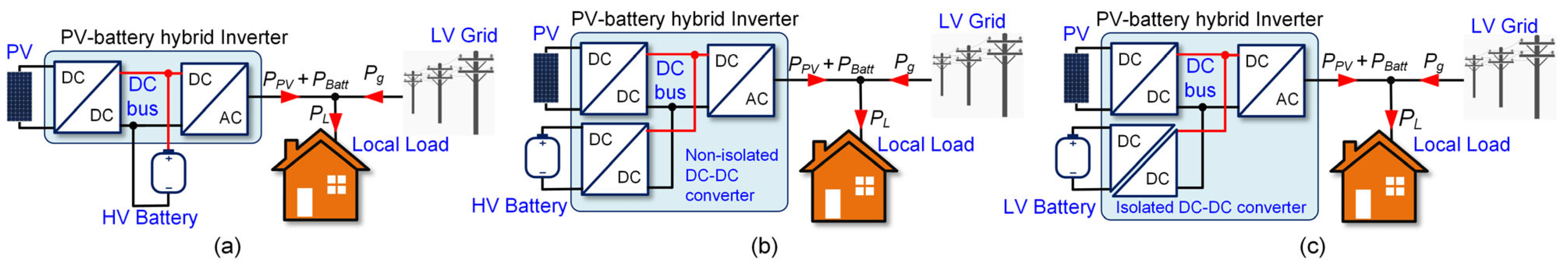
2. System Description

The main objective of this study is to design a 3 kW bidirectional inverter for interfacing a 16-cell lithium iron phosphate (LFP) battery pack with a single-phase 220 V 50 Hz grid for residential energy storage applications. Figure 3 shows the inverter topology in this study. The grid voltage v g ( t ) is converted to a 400 V DC voltage v D ( t ) through an LCL-filtered VSC. A DAB DC-DC converter well suits the second-stage battery converter as the voltage matching and galvanic isolation are achieved via the MF transformer. Moreover, if properly designed, the DAB DC-DC converter exhibits high efficiency thanks to the ZVS operation [14]. The VSC adopts the cascade control structure with the bus voltage control as the outer loop and the grid current control as the inner loop. The VSC can inject reactive power through the reference current i q ( t ) for grid support functionality. The inverse Park transformation phase-locked loop (PLL) [25] provides the estimated angle θ of the grid voltage for synchronization with the grid. The battery current i B ( t ) is regulated by a proportional-integral (PI) controller with the reference phase difference δ between the primary and secondary voltages v p ( t ) and v s ( t ) of the transformer, which are generated by the LV and HV bridges with the single-phase shift (SPS) modulation. The DC offset mitigation technique for the transformer currents i p ( t ) and i s ( t ) is implemented with the SPS modulation. The series inductor L a limits the maximum charge/discharge current [20]. The VSC and the DAB DC-DC converter’s control systems and switching signal generation are implemented on a TMS320F280049C 32-bit microcontroller from Texas Instruments (Dallas, TX, USA) [26]. Table 1 summarizes the main specifications of the battery inverter. Note that the winding resistance symbols R 1 , R a , and R g of the inductors L 1 , L a , and L g are not illustrated in Figure 1 for simplicity. Table 2 lists the parameters of the battery inverter.

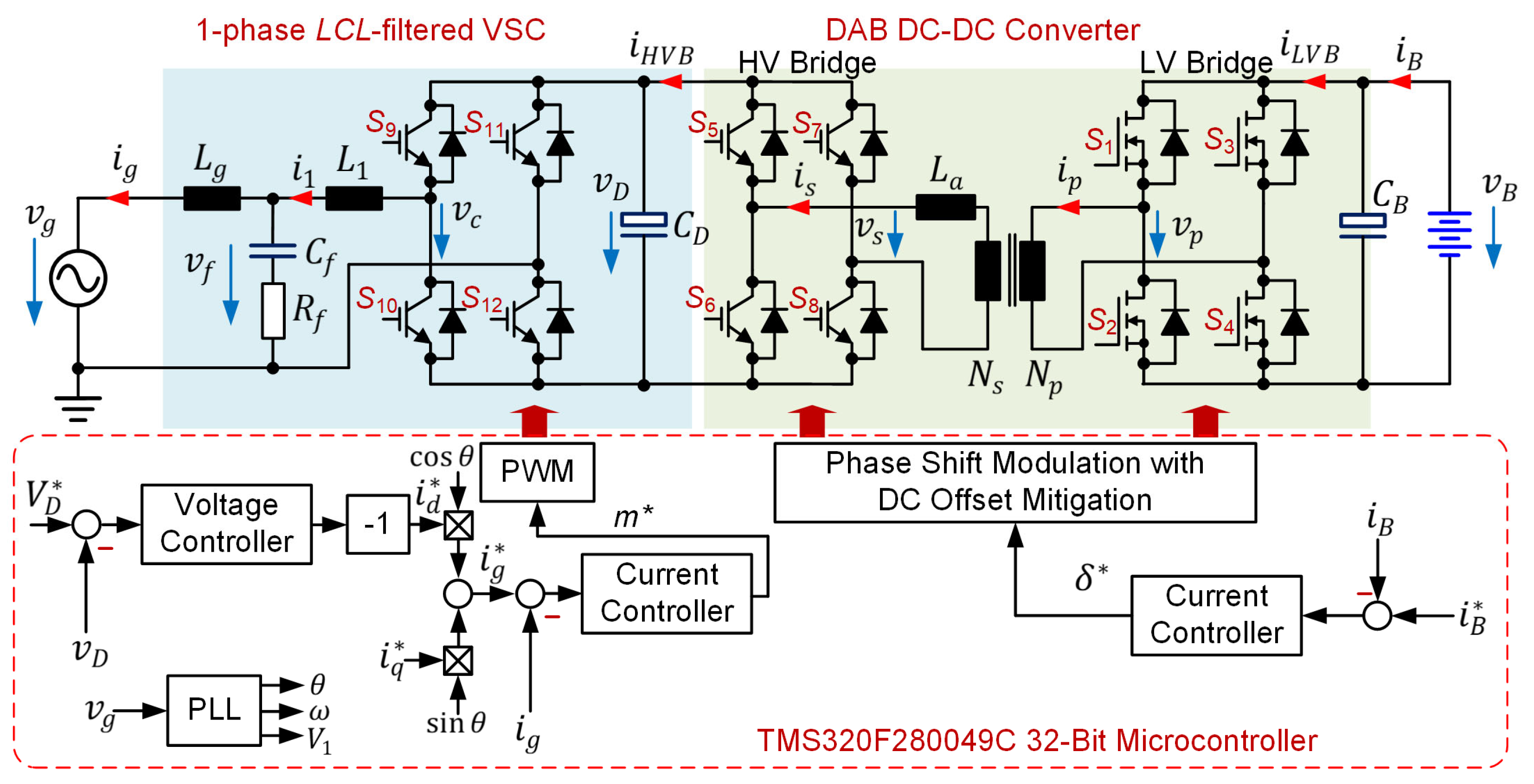
3. Implementation of the Grid-Connected VSC

3.1. VSC Modeling

The grid current i g t and bus voltage v D ( t ) of the VSC are the controlled variables. Averaging over a switching period T s w yields the governing equations for i g t as follows:
L 2 d i g ( t ) d t + R 2 i g ( t ) = v f t v g ( t ) )
v f t = v c f t + R f i 1 t i g t
C f d v c f t d t = i 1 t i g t
L 1 d i 1 t d t + R 1 i 1 t = v c t v f ( t )
v c t = d 1 t d 2 t m ( t ) v D ( t )
where v c ( t ) is the VSC terminal voltage, d 1 ( t ) and d 2 ( t ) are the duty ratios of S 9 and S 11 ranging from zero to unity, and m ( t ) is the modulation signal. The grid current typically has a faster response than the bus voltage. Thus, the instantaneous bus voltage v D ( t ) in (5) can be approximated with its average value V D . Equations (1)–(5) lead to the transfer function of the grid current given by
i g s = s C f R f + 1 C f L 1 L 2 s 3 + C f L 1 + L 2 R f s 2 + C f L 1 + L 2 s G L C L ( s ) v c s L 1 C f s 2 C f R f s + 1 + 1 G f w ( s ) v g ( s )
Neglecting power losses in the VSC and the DAB DC-DC converter, the bus voltage is governed by
v D t C D d v D t d t = p B t v c t i 1 t
where p B ( t ) is the battery power. The instantaneous power in the LCL filter is comparatively small, which yields
v c t i 1 t v g t i g t p g ( t )
where p g t is the instantaneous grid power. Substitution of (8) into (7) and linearizing around the average bus voltage setpoint V D , the bus voltage dynamic becomes
V D C D d v D t d t p B t p g t
The grid voltage is given by
v g t = V ^ 1 cos ω t
where V ^ 1 is the amplitude of the fundamental component, and ω 1 = 2 π f 1 is the fundamental frequency of the grid voltage. The grid current is usually controlled to be sinusoidal with an amplitude of I ^ 1 and a phase angle of ϕ 1 , as given by
i g ( t ) = I ^ 1 cos ( ω t + ϕ 1 )
The grid current in (11) can be decomposed to the d q axes components i d ( t ) and i q ( t ) in the virtual synchronous reference frame as
i g t = I ^ 1 cos ϕ 1 i d cos ω t I ^ 1 sin ϕ 1 i q sin ω t
The grid current in (11) leads to the instantaneous grid power expressed by
p g t = V ^ 1 2 i d P g 1 + V ^ 1 2 i d P g 1 cos 2 ω t V ^ 1 2 i q Q g 1 sin 2 ω t p ~ g 1 t
where P g 1 ( t ) and Q g 1 ( t ) are the average active and reactive power components, and p ~ g 1 ( t ) is the oscillating power component at the frequency of 2 ω . The oscillating power component p ~ g 1 ( t ) causes a 2 ω ripple component v ~ D t in the bus voltage, while the average power component P g 1 ( t ) changes the average component V D ( t ) of the bus voltage. By substituting P g 1 ( t ) in (13) into (9), V D ( t ) can be approximated as
V D C D d V D t d t P B t V ^ 1 2 i d ( t ) P g ( t )
where P B ( t ) is the average component of the battery power. Note that (14) is accurate for a frequency below 2 ω .

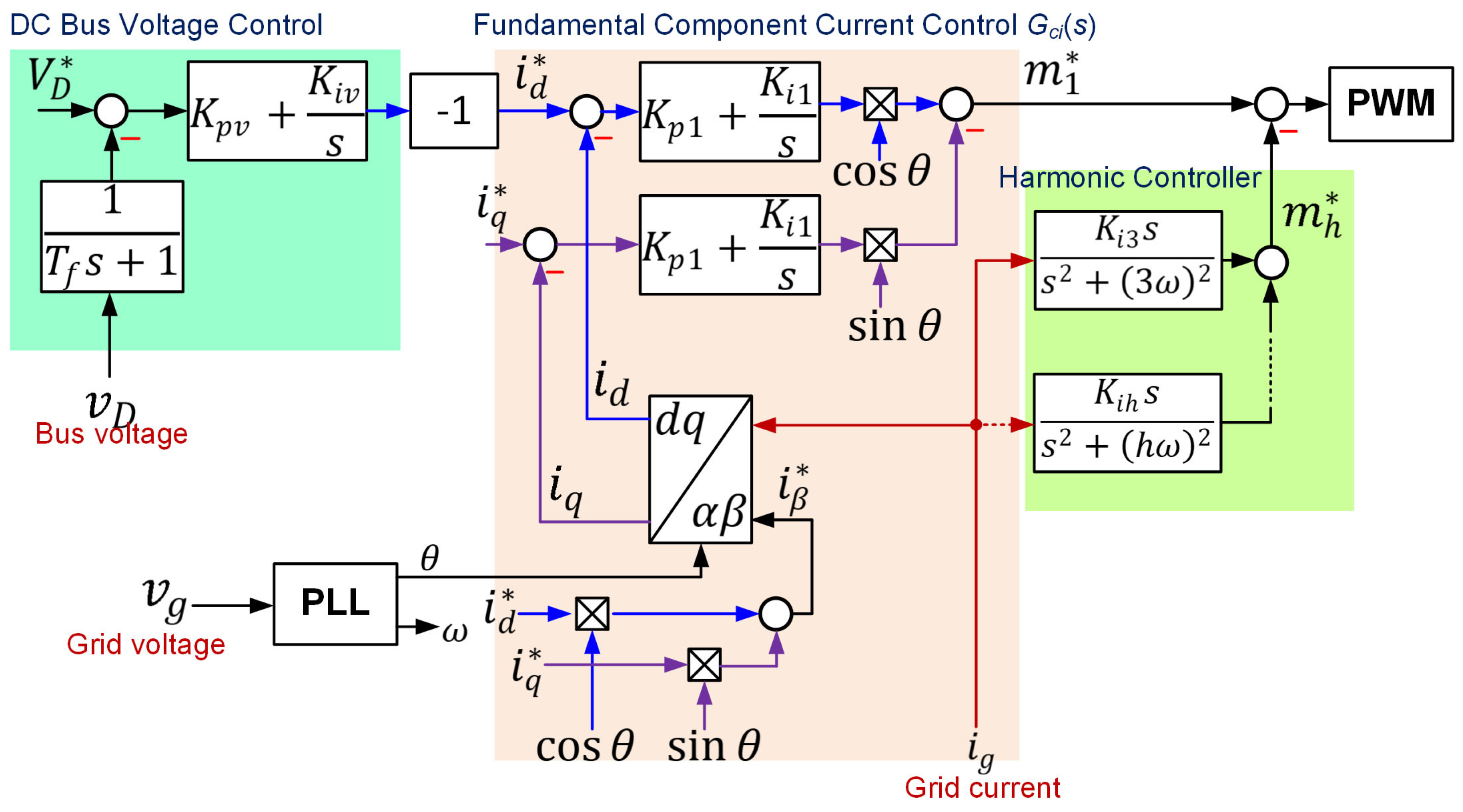
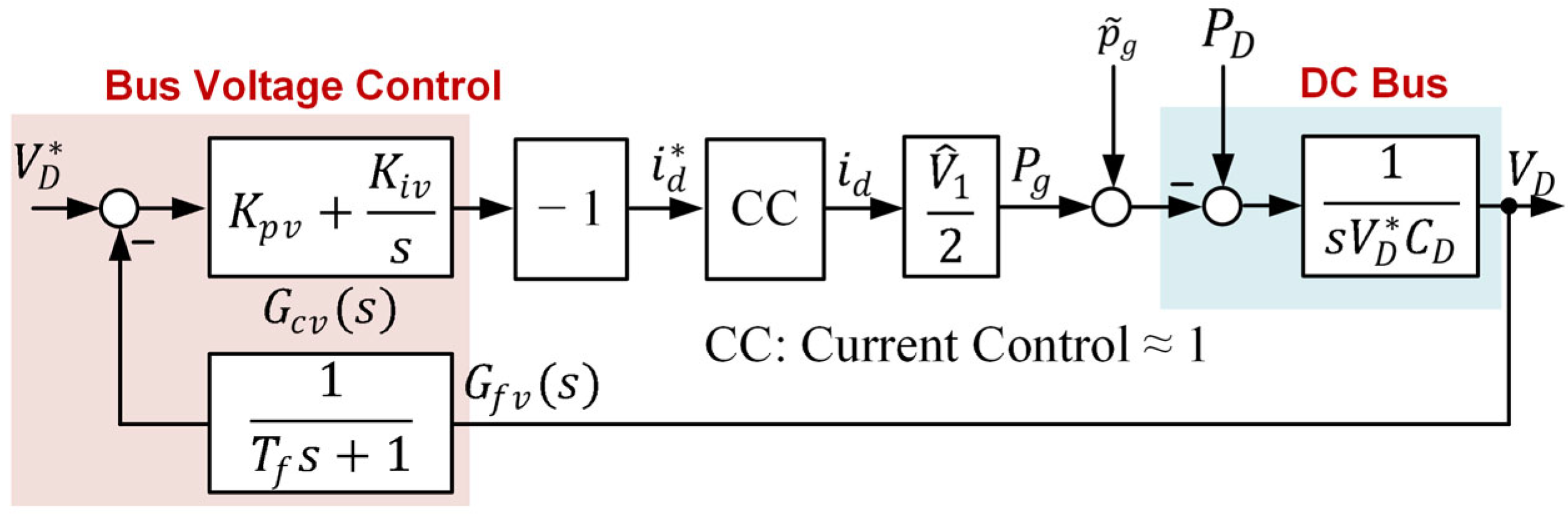
3.2. VSC Control System Implementation

Figure 4 shows the VSC control system. A proportional-integral (PI) regulator is employed for the bus voltage control loop with a low-pass filter (LPF) for shaping the loop frequency response. Meanwhile, the grid current controller adopts the unbalanced synchronous reference frame control with PI regulators for the fundamental component. This control technique employs the grid current as the α -component and the orthogonal reference current i β ( t ) as the β -component for the axis transformation. In our previous work [24], the stationary reference frame equivalence G c i 1 ( s ) of the unbalanced synchronous reference frame control with the PI regulators was theoretically and experimentally proven to be identical to a proportional-resonant regulator, as given by
G c i 1 s = K p 1 + K i 1 s s 2 + ω 2
where K p 1 and K i 1 are the proportional and integral gains of the PI controller. Three possible harmonic sources distort the grid current waveforms, which can be suppressed by multiple resonant (MR) controllers given by
G c i h s = h = 3 n K i h s s 2 + h ω 2
where h is the harmonic order number, and K i h is the resonant gain at order h t h .
Figure 5 depicts the stationary reference frame’s equivalent grid current control block diagram. The VSC is represented by
G P W M s = V D e s T d
where T d is the delay time caused by the sampling time of the control system and the transportation time of the pulse width modulation (PWM) process. Undesirable low-frequency harmonic components can be present in the grid voltage v g ( t ) and in the VSC terminal voltage v c ( t ) due to switching dead times. The 2 ω ripple component in the bus voltage control loop with a bandwidth greater than 0.2 ω also distorts the reference current i g ( t ) [24]. With this current control structure, the transfer functions of the grid current to these three harmonic sources are written as follows [24].
G c l s = i g ( s ) i g ( s ) = G c i s G P W M s G L C L ( s ) 1 + G c i s + G c i h s G P W M s G L C L ( s )
Y V S C s = i g s v c ( s ) = G L C L ( s ) 1 + G c i s + G c i h s G P W M s G L C L ( s )
Y g ( s ) = i g s v g ( s ) = G F W ( s ) G L C L ( s ) 1 + G c i s + G c i h s G P W M s G L C L ( s )
The MR regulator has infinite gains at selective frequencies, attenuating the harmonic components in i g ( t ) , v g ( t ) , and v c ( t ) . Meanwhile, the fundamental component of i g ( t ) is regulated by the unbalanced synchronous reference frame controller with an infinite gain at ω 1 . Figure 6 depicts the equivalent bus voltage control loop. The low-pass filter time constant T f designed with the PI controller’s constants K p v and K i v is used for loop shaping. The grid current control loop is approximated as a unity gain because its bandwidth is far higher than the bus voltage control loop. The rejection of the harmonic components in the reference current allows the bandwidth of the bus voltage control loop to increase while maintaining the grid current near sinusoidal.
This study employs the discontinuous PWM techniques shown in Figure 7. The positive half of m ( t ) is used as the duty ratio reference for switches S 9 and S 10 , and the positive half of − m ( t ) for switches S 11 and S 12 . This PWM technique has a lower common-mode voltage and switching loss than the unipolar PWM [27]. Meanwhile, the VSC current i 1 ( t ) maintains a small ripple due to the three-level voltage output at the VSC terminal. Figure 8 illustrates the generation of the switching signals and interrupt setting. Time base counter 1 of the microcontroller [26] is set to operate in the up-down mode with the counter maximum value of PWMprd, which generates the interrupt signal when the counter value equals zero. The value of PWMprd is obtained from
P W M p r d = 1 2 × f c l k f s w
where f c l k = 100 MHz is the microcontroller’s clock frequency [26]. Thus, PWMprd = 2500 for a switching frequency of 20 kHz. This interrupt signal simultaneously triggers the selected analog-to-digital converters (ADCs) for voltage and current signal sampling at the time instant k and the interrupt service routine (ISR) of the control algorithm for the VSC and DAB DC-DC converter. The resultant duty ratios are updated at the time instant k + 1 . Each counter consists of two compare registers (CMPAx and CMPBx), independently controlling two PWM outputs (PWMxA and PWMxB). For the VSC control, only CMPAx registers generate the PWMxA outputs, while the PWMxB outputs are opposite to the relevant PWMxA outputs with a switching dead time (active high complementary with a dead time) [26]. Thus, the PWM1A and PWM1B outputs of counter 1 control switches S 9 and S 10 , and the PWM2A and PWM2B outputs of counter 2 for switches S 11 and S 12 . The synchronized operation between the ADC and PWM samples the average value of the grid current in each switching period both for the positive and negative regions of the modulation signal, as illustrated in Figure 8.

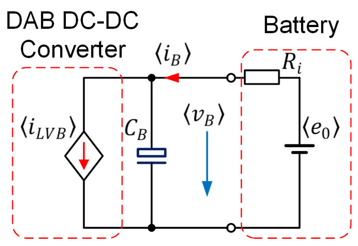
4. Implementation of the Battery-Side DAB DC-DC Converter

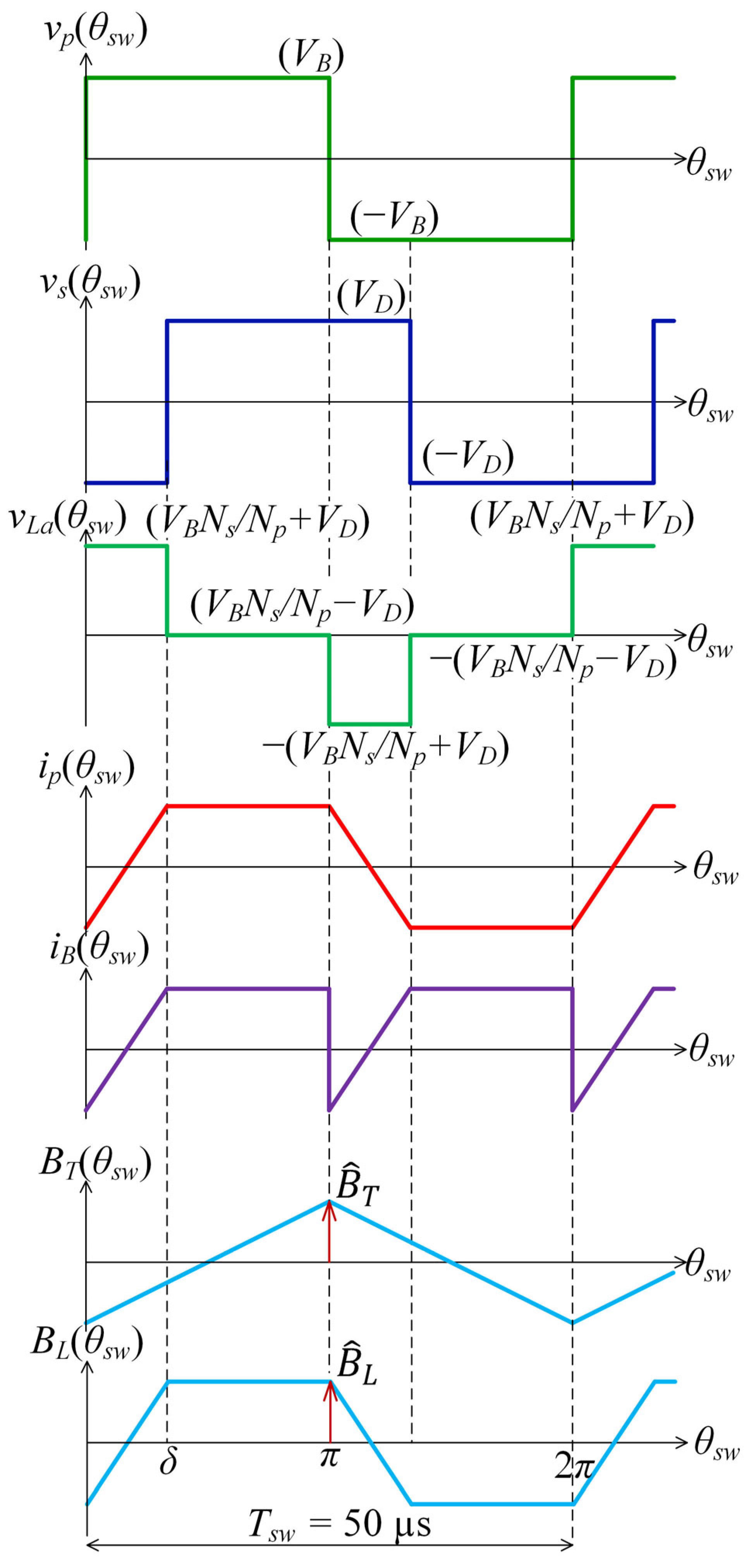
4.1. Basic Operation of the DAB DC-DC Converter

Figure 9 illustrates the basic operation waveforms of the DAB DC-DC converter in the SPS modulation mode, where ω s w = 2 π f s w and θ s w = ω s w t . The voltage v P ( θ s w ) of the LV bridge leads the voltage v s ( θ s w ) of the HV bridge by a phase angle of δ , which causes power to flow from the battery to the bus voltage. On the other hand, power transfers from the bus voltage to the battery with a phase angle of δ . Thus, the transferred power P D A B of the DAB DC-DC converter is controlled by the angle δ by
P D A B = V D N s N p V B ω s w L a δ 1 δ π
Neglecting losses in the DAB DC-DC converter, the average value I L V B of the LV bridge input current i L V B and the average battery current I B are derived from P D A B by
I B = I L V B = P D A B V B = N s N p V D ω s w L a δ 1 δ π
Hence, the phase angle δ is used as the controlled variable for the battery current control loop as shown in Figure 3. The theoretical range of the phase angle δ is ± π / 2 . The DAB DC-DC converter exhibits the ZVS operation if the ratio between the voltages of the two DC sides is close to the transformer’s turn ratio [28]. This ZVS range gets wider at a higher phase shift angle [14]. On the other hand, the root mean square (RMS) values of the MF transformer’s currents increase with the phase shift angle [10].
Flux density B ( t ) is an essential parameter for the design of the MF transformer and series inductor. According to the circuit topology in Figure 3, the transformer’s primary winding is directly connected to the LV bridge. So, the peak flux density B ^ T of the transformer is proportional to the battery voltage, as given by
B ^ T = 1 2 N p A c 0 T s w / 2 v p d t = V B T s w 4 N p A c
where A c is the cross-sectional area of the transformer core. Meanwhile, the peak flux density B ^ L of the series inductor is determined from the voltage across the inductor v L a ( θ s w ) in Figure 9, as given by
B ^ L = 1 2 N L A c 0 T s w / 2 v L a d t = T s w 4 N L A c π N s N p V B + 2 δ π V D
where N L is the winding turn number of the inductor. The peak flux densities B ^ T and B ^ L must be kept below the saturation flux density B ^ s a t of the core material.

4.2. Design of the Transformer and Series Inductor

The MF transformer of the DAB DC-DC converter is a crucial element for transferring power and voltage conversion between the two DC sides. Meanwhile, the series inductor L a limits the maximum power transfer. MnZn ferrite and nanocrystalline materials are suitable for the switching frequency of 20 kHz used in this study. For this application, the battery voltage varies with the state of charge and battery current, while the bus voltage is kept constant. Thus, the maximum allowable phase shift angle is ±π/3 to exploit a large ZVS range at the rated power and achieve a fine battery current resolution, while the RMS values of the transformer currents are still acceptable. It was reported that nanocrystalline materials exhibited better power density and efficiency than MnZn ferrite material [10]. However, the cutting process of ribbon-wound nanocrystalline cores deteriorated their magnetic properties [10]. Hence, we selected N87 MnZn ferrite cores due to consistency in magnetic properties and market availability [29]. This core material has a saturation flux density of 0.39 T at 100 °C and is available in various core shapes.
An analytical transformer and inductor design method was chosen in this study [30]. The generalized Steinmetz equation expresses the core loss P f e as a function of the core peak flux density B ^ . Meanwhile, the copper loss P c u is derived from the RMS values of the transformer’s currents and the winding resistance. Therefore, the winding resistance is derived from the core geometry, which is expressed as a function of the core peak flux density B ^ . Setting P f e = P c u leads to the optimal peak flux density B ^ o p t , from which the minimum core size is obtained. An actual core size should be selected close to the optimal one.
The MF transformer and the inductor were designed at the nominal battery voltage V B n of 51.2 V using the peak flux densities given in (24) and (25). The transformer turn ratio is close to
N s N p = V D V B n = 400   V 51.2   V = 7.81
The peak flux densities B ^ T and B ^ L calculated at the maximum battery voltage of 60 V were ensured to be below the core saturation value. The core loss coefficient was identified from the manufacturer’s specification at the temperature of 100 °C. Enameled Litz wires were employed to minimize the skin and proximity effects from the switching frequency. The required value of L a obtained from (23) is 297 μH. However, the inductance of 280 μH was used in the design to account for the leakage inductance of the MF transformer. Table 3 summarizes the key parameters of the MF transformer and series inductor. The actual core sizes are slightly larger than the required sizes. Thus, the peak flux densities B ^ T and B ^ L are smaller than their optimal values. This results in the estimated core losses being comparatively less than the copper losses. The predicted core loss using the generalized Steinmetz equation is based on the sinusoidal induction waveform. Moreover, the N87 ferrite material has a more significant core loss at low temperatures. In experiments, the core temperature was found to be lower than 60 °C, which agrees with our previous work with the same design methodology and core material [10]. Thus, the actual core losses are expected to exceed the predicted values.

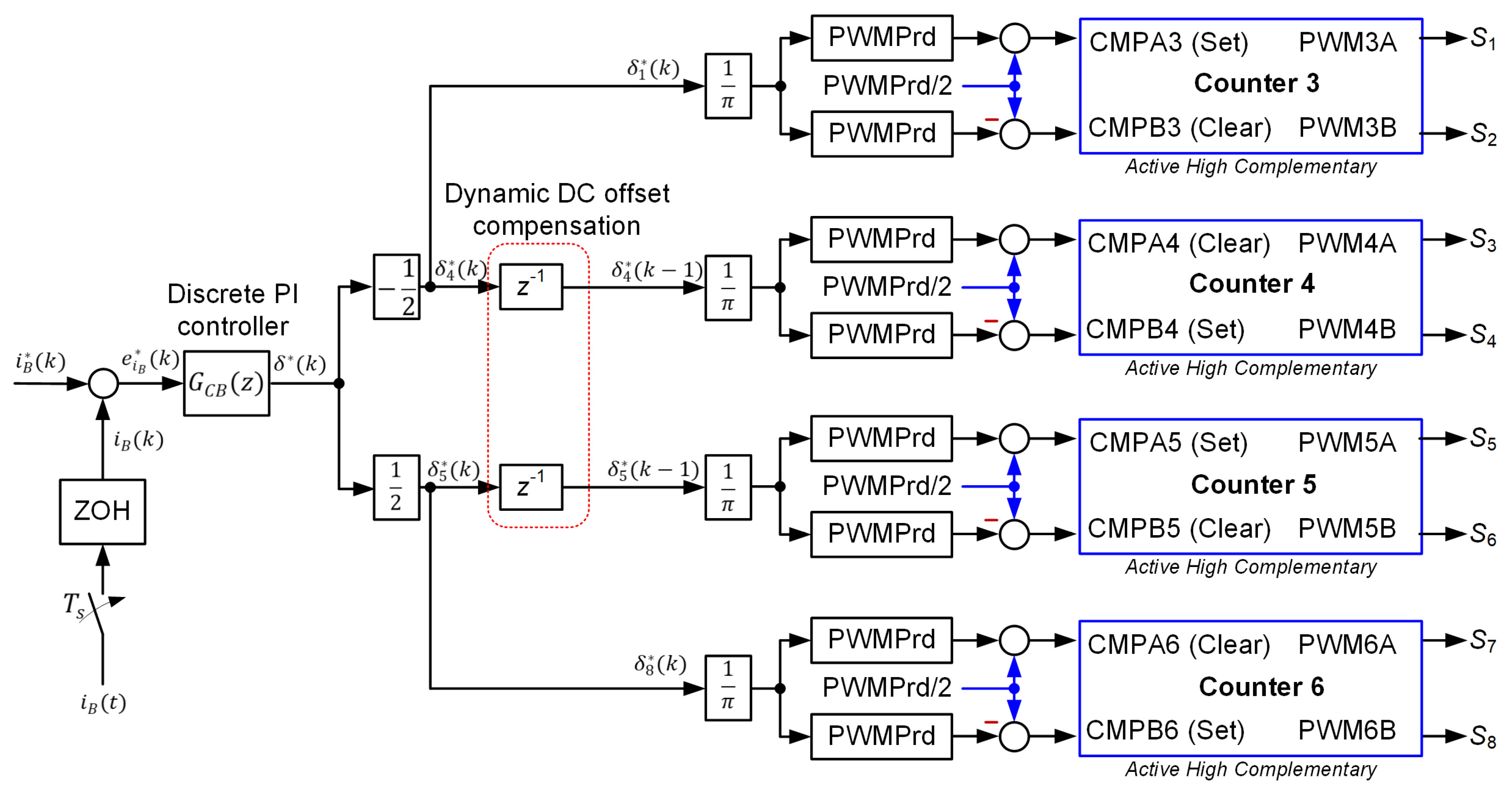
4.3. Control System Implementation of the DAB DC-DC Converter

Figure 10 sketches the steady state timing diagram of the DAB DC-DC converter, implemented in the same ISR as the VSC control scheme in Figure 8. Counters 3–6 in the up-down mode generate the switching signals for the DAB DC-DC converter. The phase angles of counters 3–6 are synchronized with counter 1. Instead, the phase shift modulation is obtained by adjusting the CMPA3 to CMPA6 and the CMPB3 to CMPB6 registers of counters 3–6 [31]. During the rising period of counters 3–6, switches S 1 , S 4 , S 5 , and S 8 are turned on when the values of the counters equal their CMPAs registers. For the falling period, switches S 1 , S 4 , S 5 , and S 8 are turned off when the values of the counters equal their CMPBs registers. Thus, this modulation strategy accommodates the maximum phase shift angle of ±π/2. Note that switches S 2 , S 3 , S 6 , and S 7 complement switches S 1 , S 4 , S 5 , and S 8 respectively.
The phase shift angle δ = 0 is set at π / 2 of each ISR period to sample the average value of the battery current i B ( t ) . The reference phase angles δ 1 and δ 4 for switches S 1 and S 4 of the LV bridge and δ 5 and δ 8 for switches S 5 and S 8 of the HV bridge are obtained from
δ 1 = δ 4 = δ 2 δ 5 = δ 8 = δ 2
where δ is the reference phase shift angle. Figure 9 shows the implementation diagram of the battery current control. The battery current is sampled every T s . The discrete-time PI controller G C B ( z ) regulates the battery current i B k at instant k with the reference phase angle δ k as the output. The reference angles δ 1 ( k ) , δ 4 ( k ) , δ 5 ( k ) , and δ 8 ( k ) are obtained from (27). The reference angles δ 1 ( k ) and δ 8 ( k ) are translated to the values of the CMPA3, CMPB3, CMPA6, and CMPB6 registers as depicted in Figure 11. Meanwhile, the reference angles δ 4 ( k ) and δ 5 ( k ) are delayed with a sampling period to prevent a large DC offset current in the transformer current i p ( t ) during the transient [20]. This method is to control the volt-second applied to the transformer to maintain a small DC offset. So, the values of CMPA4, CMPB4, CMPA5, and CMPB5 are accordingly determined from δ 4 ( k 1 ) and δ 5 ( k 1 ) . The action qualifier submodule of each module defines the action of the PWMxA output when the CMPAx and CMPBx registers meet their conditions as indicated by “set” and “clear” in the brackets. Meanwhile, the PWMxB outputs are opposite to their PWMxA outputs, with a dead time of 1.25 μs similar to that of the VSC [26].

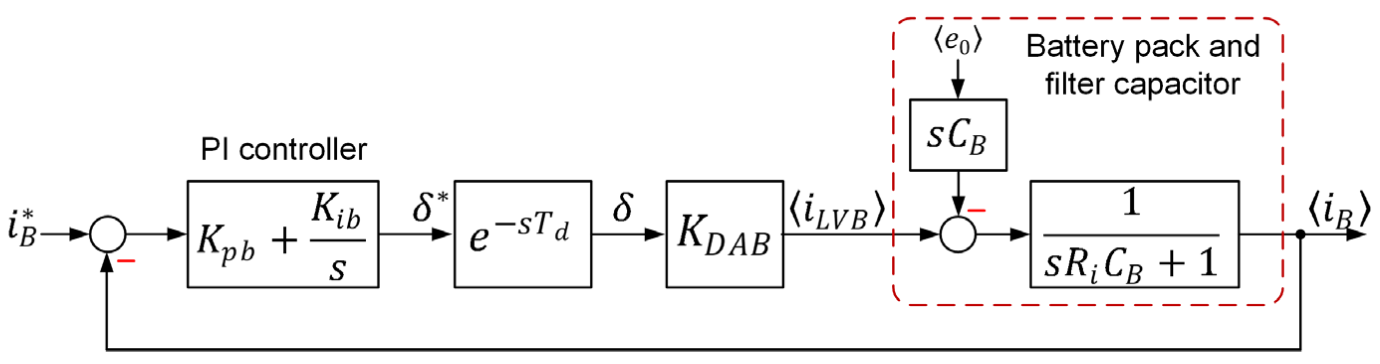
4.4. Tuning of the Battery Current Control Loop

Figure 12 depicts the equivalent circuit on the battery side. The variables are averaged over a switching period of T s w , denoted by the brackets 〈 〉. Equation (23) yields the average current i L V B of the DAB DC-DC converter, while the battery is simplified with an open-circuit voltage e 0 and an internal resistance R i . The Thevenin-based equivalent circuit consisting of internal series resistance and capacitance paralleled with another resistance is more accurate than that in Figure 12 [32]. The Thevenin-based capacitance is much larger than the battery-side capacitance C B [33]. From the control point of view, thus, the open-circuit voltage e 0 in Figure 12 including the voltage drops in the Thevenin-based capacitance is the disturbance of the battery current control loop. Figure 13 depicts the equivalent block diagram of the battery current in the continuous time domain, where a PI regulator with the constants K p b and K i b controls the battery current. A delay of T d = 2 T s represents the sampling and transport delays, as illustrated in Figure 10. The gain K D A B is derived from the possible maximum value of (23), as given by
K D A B = i L V B δ = N s N p V D ω s w L a
According to (23), this gain K D A B decreases with the angle δ for a higher battery current. However, the approximated gain K D A B at its maximum value guarantees the maintenance of loop stability at a high current.
The open loop transfer function of the battery current control loop is written as
G b o l s = K p b + K i b s K D A B s R i C B + 1
where the delay T d is neglected as it usually is much smaller than the time constant R i C B . The closed-loop transfer function is given as
G b c l s = K D A B R i C B s + K i K D A B R i C B s 2 + 1 + K p b K D A B R i C B s + K i K D A B R i C B
Compared to the standard second-order system [34], K p b and K i b can be written as
K i b = ω 0 2 R i C B K D A B K p b = 2 ξ ω 0 R i C B 1 K D A B
where ω 0 is the natural frequency, and ξ is the damping factor of the closed-loop system. If R i is unknown, a trial-and-error tuning method can be adopted by adjusting K i b for ω 0 2 and K p b for ξ .

5. Experimental Validation

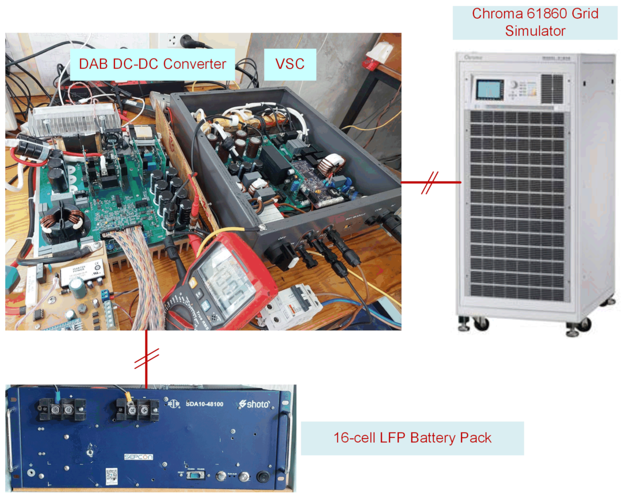
5.1. Experimental Setup

Figure 14 depicts the experimental setup. A TMS320F280049C microcontroller controlled the VSC and DAB DC-DC converter with the parameters listed in Table 2. A switching dead time of 1.25 μs was applied to each leg of the VSC and DAB DC-DC converter. A 16-cell 100 Ah LFP battery pack supplied the DAB DC-DC converter, while the VSC was connected to a Chroma 61860 grid simulator. We adopted the tuning procedure of the VSC presented in our previous work [24] with a bus voltage bandwidth of 30π rad/s and the current harmonic controllers, orders 3rd, 5th, 7th, and 9th for mitigation of the grid current waveform. The bus voltage was regulated at 400 V. The response of the battery current was tuned by the trial-and-error method with the guidelines given in (31). The battery management system has a maximum current of 30 A, which, unfortunately, limits the maximum system power within ±1.5 kW or 50% of the rated power.

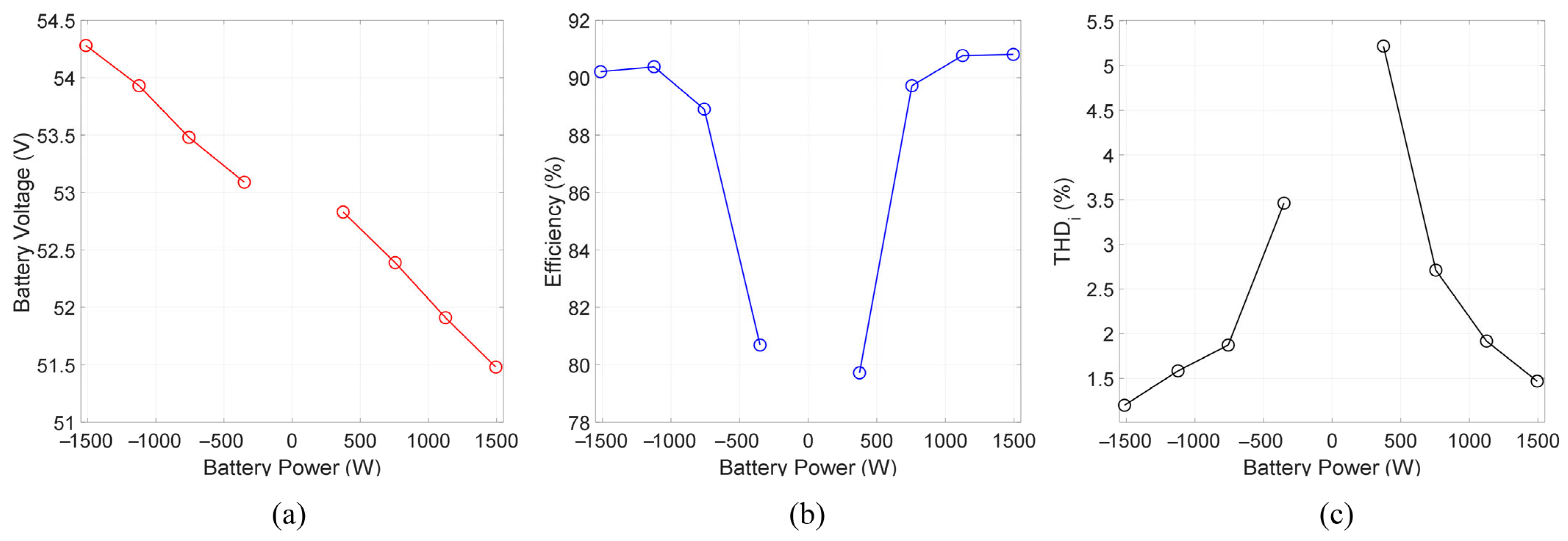
5.2. Experimental Results

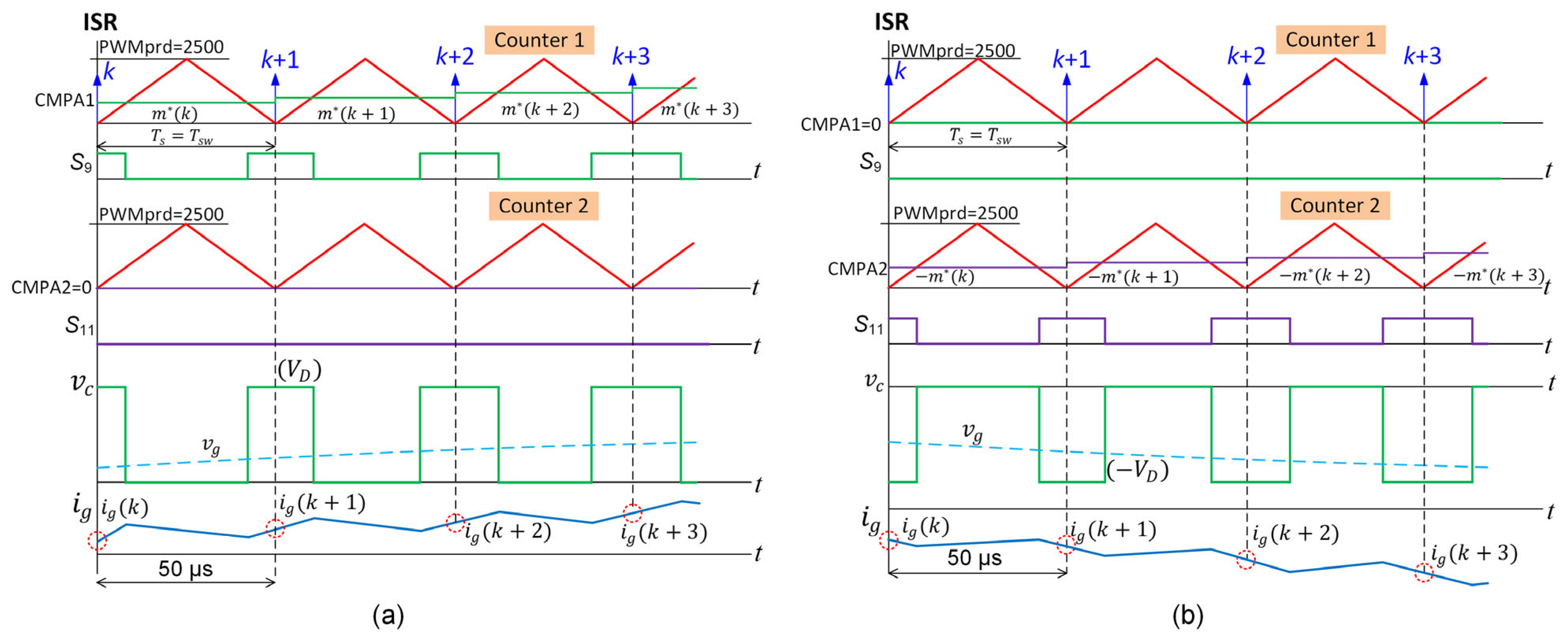
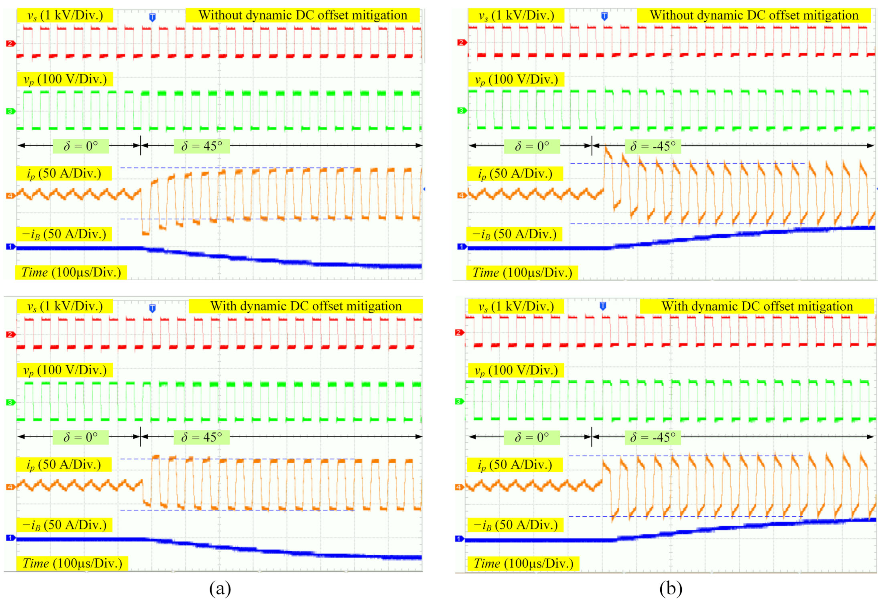
5.2.1. Validation of the Dynamic DC Offset Compensation Scheme

The grid simulator supplied the VSC, and the bus voltage was regulated at 400 V. The DAB DC-DC converter operated with the reference phase angle δ in the open-loop control. Figure 15a depicts the transient response of the primary and secondary voltages v p ( t ) and v s ( t ) , the transformer’s primary current i p ( t ) , and the inverted battery current i B ( t ) under the step change of the reference angle δ changing from zero to π/4. In contrast, Figure 15b shows those waveforms for the reference angle δ changing from zero to −π/4. Without the dynamic DC offset compensation scheme shown in Figure 11, i p ( t ) exhibits a DC offset of approximately 30 A. This large current can cause saturation in the transformer core and may damage the switching devices. The DC offset compensation technique in Figure 11 is effective as the dynamic DC component of i p ( t ) is reduced significantly during the changes in the reference angle δ . Meanwhile, the DC offset compensation scheme does not affect the steady waveform of i p ( t ) . The first-order response of the battery current i B ( t ) agrees with the equivalent circuit in Figure 12.

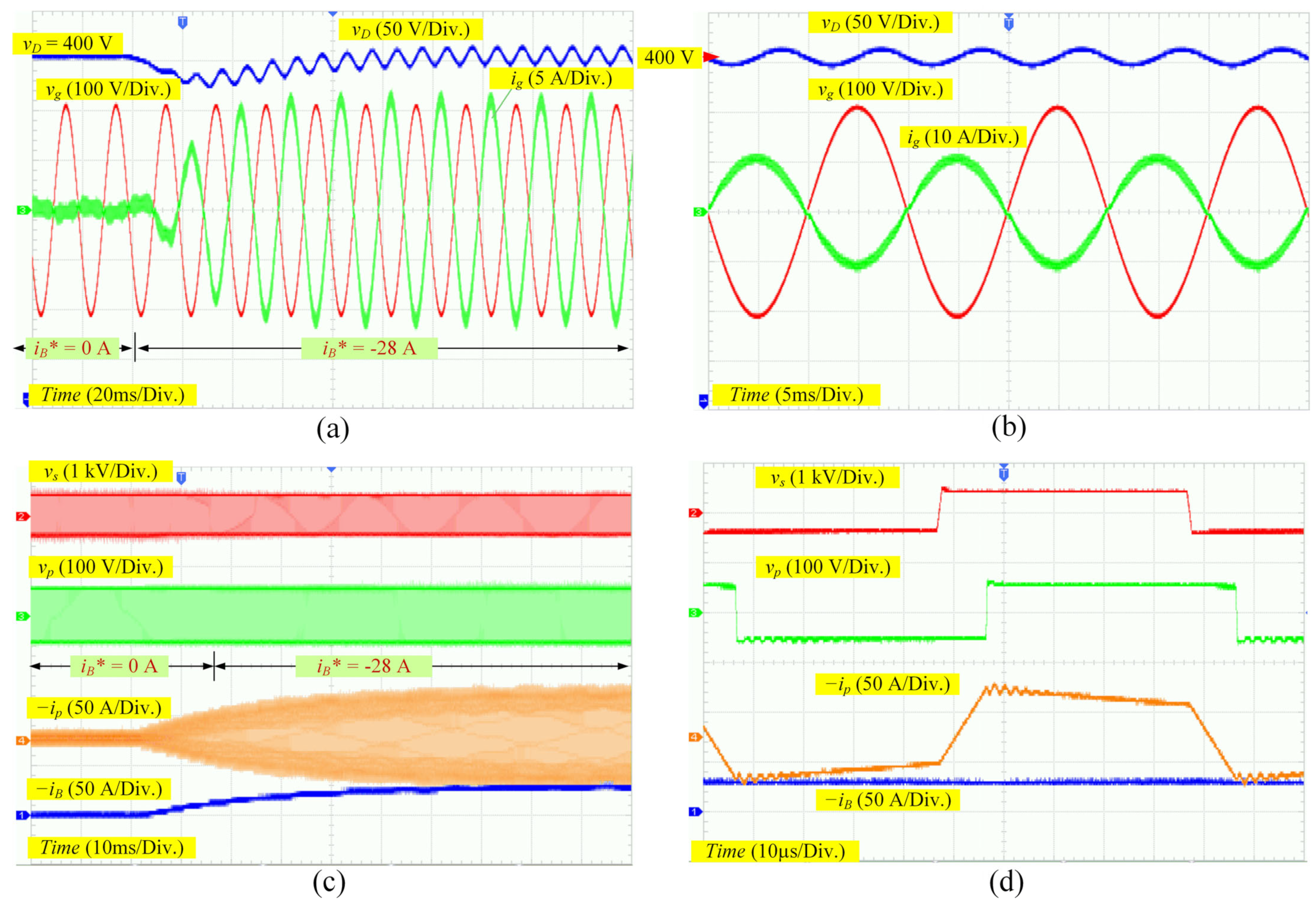
5.2.2. Validation of the Closed-Loop Control of the Battery Current

The battery current control loop was tuned for a smooth response with a settling time of approximately 80 ms. The reference battery current i B was set to create the battery power in the range of ±1.5 kW. Figure 16 shows the experimental results in the discharging mode with a battery power of 1.5 kW. Although the discharged power from the battery causes the bus voltage to increase, the bus voltage controller forces the bus voltage to return to the reference of 400 V within four cycles, as shown in Figure 16a. Figure 16b depicts the steady-state waveforms of v D ( t ) , v g ( t ) , and i g ( t ) . The grid current waveform is nearly sinusoidal thanks to the current harmonic current controller, which attenuates the harmonic components in the reference grid current and the VSC terminal voltage caused by the dead time. Figure 16c illustrates that a step change in the battery reference current i B does not create a DC offset in the transformer’s primary current i p ( t ) , thanks to the DC offset compensation scheme implemented in the SPS modulation system in Figure 11. Meanwhile, the battery current i B ( t ) smoothly increases toward its reference. The steady-state waveforms of v p ( t ) , v s ( t ) , and i p ( t ) in Figure 16d agree with the sketched waveforms in Figure 10. At this operating point, the battery voltage was 51.5 V, close to the designed value of the MF transformer.
Figure 17 shows the experimental results in the charging mode with a battery power of −1.5 kW. The bus voltage v D ( t ) , grid current i g ( t ) , transformer’s primary current i p ( t ) , and battery current i B ( t ) respond to the battery reference current i B in the same fashion as the discharging mode with the opposite direction. The steady-state grid current waveform remains nearly sinusoidal. However, the steady-state waveform of i p ( t ) indicates that the DAB DC-DC converter operates in the boost mode, where N s / N p V B > V D [19]. At this operating point, the battery voltage was 54.3 V, causing N s / N p V B = 424 V.
Figure 18 shows the battery voltage, total efficiency of the VSC and DAB DC-DC converter, and total harmonic distribution (THDi) of grid current with battery power. As expected, the battery voltage in the charging mode is greater than that in the discharging mode. The inverter’s efficiency in the charging mode is lower than in the discharging mode. Partly, it is believed to be due to the mismatched voltage ratio of the MF transformer, which deviates the operating point out of the ZVS region o and increases RMS values in the transformer currents [28]. Thus, a variable DC voltage strategy with the battery voltage and a duty ratio adjustment of the transformer would improve the inverter’s efficiency. The THDi values at 50% of the rated power are less than 1.5%, which are expected to be lower at the rated power of 3 kW.

6. Conclusions and Future Outlook

A single-phase grid-connected 51.2-V battery inverter consisting of an LCL-filtered voltage source converter (VSC) and a dual active bridge (DAB) DC-DC converter was constructed. The control systems of the two converters were implemented in the same interrupt service routine on a TMS320F280049C microprocessor with a sampling and switching frequency of 20 kHz—the time base counters for switching generation of the DAB DC-DC converter synchronized with those of the VSC. The single-phase shift modulation strategy of the DAB DC-DC converter was adjusted through two separate compare registers with the time base counters during the count-up and count-down periods. This phase shift modulation was easy to implement on a standard microcontroller for power converter control. A DC offset compensation integrated with the battery current control loop allowed a smooth change in the battery and medium-frequency transformer’s currents in response to a reference current step. The VSC adopted a bus voltage control with a unified harmonic mitigation strategy. Experimental validations in the charge and discharge operations exhibited a total system efficiency better than 90% and total harmonic distortion in the grid current lower than 1.5%.
However, certain aspects must be studied further to improve the proposed residential battery inverter as follows:
(1)
Adoption of advanced battery current control schemes regardless of the battery’s internal impedance parameters.
(2)
Increasing the switching frequency and improving the modulation strategies of the DAB DC-DC converter to enhance efficiency and power density.
(3)
Optimizing the design of the ripple filter on the battery side.

Author Contributions

Conceptualization, A.P. and S.S.; methodology, A.P. and S.S.; software, A.P. and T.K.; validation, A.P., T.K. and C.S.; formal analysis, A.P., S.S., P.P. and M.H.; investigation, A.P. and S.S.; resources, S.S.; data curation, A.P.; writing—original draft preparation, A.P. and S.S.; writing—review and editing, S.S., P.P. and M.H.; visualization, A.P. and T.K.; supervision, S.S.; project administration, S.S.; funding acquisition, S.S. All authors have read and agreed to the published version of the manuscript.

Funding

This research was partially supported by the Royal Golden Jubilee Ph.D. Program, grant number PHD02282560, and the Global and Frontier Research University Fund, Naresuan University, grant number R2567C002.

Data Availability Statement

The data presented in this study is available in the article.

Conflicts of Interest

The authors declare no conflict of interest.

References

  1. Renewables 2023-Analysis and Forecast to 2028. Available online: https://iea.blob.core.windows.net/assets/96d66a8b-d502-476b-ba94-54ffda84cf72/Renewables_2023.pdf (accessed on 4 February 2024).
  2. Hu, J.; Li, Z.; Zhu, J.; Guerrero, J.M. Voltage Stabilization: A Critical Step Toward High Photovoltaic Penetration. IEEE Ind. Electron. Mag. 2019, 13, 17–30. [Google Scholar] [CrossRef]
  3. IRENA. Innovation Landscape Brief: Utility-Scale Batteries. Available online: https://www.irena.org/-/media/Files/IRENA/Agency/Publication/2019/Sep/IRENA_Utility-scale-batteries_2019.pdf (accessed on 4 February 2024).
  4. Riyaz, A.; Sadhu, P.K.; Iqbal, A.; Alamri, B. Comprehensive Survey of Various Energy Storage Technology Used in Hybrid Energy. Electronics 2021, 10, 2037. [Google Scholar] [CrossRef]
  5. Ko, J.-S.; Huh, J.-H.; Kim, J.-C. Overview of Maximum Power Point Tracking Methods for PV System in Micro Grid. Electronics 2020, 9, 816. [Google Scholar] [CrossRef]
  6. Ahmed, M.; Harbi, I.; Kennel, R.; Heldwein, M.L.; Rodríguez, J.; Abdelrahem, M. Performance Evaluation of PV Model-Based Maximum Power Point Tracking Techniques. Electronics 2022, 11, 2563. [Google Scholar] [CrossRef]
  7. Galkin, I.A.; Blinov, A.; Vorobyov, M.; Bubovich, A.; Saltanovs, R.; Peftitsis, D. Interface Converters for Residential Battery Energy Storage Systems: Practices, Difficulties and Prospects. Energies 2021, 14, 3365. [Google Scholar] [CrossRef]
  8. Cao, J.; Emadi, A. Batteries Need Electronics. IEEE Ind. Electron. Mag. 2011, 5, 27–35. [Google Scholar] [CrossRef]
  9. Biao, Z.; Qiang, S.; Wenhua, L.; Yandong, S. Overview of Dual-Active-Bridge Isolated Bidirectional DC-DC Converter for High-Frequency-Link Power-Conversion System. IEEE Trans. Power Electron. 2014, 29, 4091–4106. [Google Scholar] [CrossRef]
  10. Somkun, S.; Sato, T.; Chunkag, V.; Pannawan, A.; Nunocha, P.; Suriwong, T. Performance Comparison of Ferrite and Nanocrystalline Cores for Medium-Frequency Transformer of Dual Active Bridge DC-DC Converter. Energies 2021, 14, 2407. [Google Scholar] [CrossRef]
  11. Lo Franco, F.; Morandi, A.; Raboni, P.; Grandi, G. Efficiency Comparison of DC and AC Coupling Solutions for Large-Scale PV+BESS Power Plants. Energies 2021, 14, 4823. [Google Scholar] [CrossRef]
  12. Duracell Energy Bank. Available online: https://www.duracellenergybank.com/ (accessed on 4 February 2024).
  13. What to Expect for Powerwall 3. Available online: https://www.tesla.com/support/energy/powerwall/learn/what-expect-powerwall-3 (accessed on 4 February 2024).
  14. Kheraluwala, M.N.; Gascoigne, R.W.; Divan, D.M.; Baumann, E.D. Performance characterization of a high-power dual active bridge DC-to-DC converter. IEEE Trans. Ind. Appl. 1992, 28, 1294–1301. [Google Scholar] [CrossRef]
  15. Jin, N.-Z.; Feng, Y.; Chen, Z.-Y.; Wu, X.-G. Bidirectional CLLLC Resonant Converter Based on Frequency-Conversion and Phase-Shift Hybrid Control. Electronics 2023, 12, 1605. [Google Scholar] [CrossRef]
  16. Zhou, K.; Sun, Y. Research on Bidirectional Isolated Charging System Based on Resonant Converter. Electronics 2022, 11, 3625. [Google Scholar] [CrossRef]
  17. Shu, L.; Chen, W.; Song, Z. Prediction method of DC bias in DC-DC dual-active-bridge converter. CPSS Trans. Power Electron. Appl. 2019, 4, 152–162. [Google Scholar] [CrossRef]
  18. Wang, Z.; Chai, J.; Sun, X. Method to control flux balancing of high-frequency transformers in dual active bridge dc–dc converters. J. Eng. 2018, 2018, 1835–1843. [Google Scholar] [CrossRef]
  19. Guzmán, P.; Vázquez, N.; Liserre, M.; Orosco, R.; Pinto Castillo, S.E.; Hernández, C. Two-Stage Modulation Study for DAB Converter. Electronics 2021, 10, 2561. [Google Scholar] [CrossRef]
  20. Takagi, K.; Fujita, H. Dynamic Control and Performance of a Dual-Active-Bridge DC–DC Converter. IEEE Trans. Power Electron. 2018, 33, 7858–7866. [Google Scholar] [CrossRef]
  21. Karimi-Ghartemani, M.; Khajehoddin, S.A.; Jain, P.; Bakhshai, A. A systematic approach to DC-bus control design in single-phase grid-connected renewable converters. IEEE Trans. Power Electron. 2013, 28, 3158–3166. [Google Scholar] [CrossRef]
  22. Somkun, S.; Srita, S.; Kaewchum, T.; Pannawan, A.; Saeseiw, C.; Pachanapan, P. Adaptive Notch Filters for Bus Voltage Control and Capacitance Degradation Prognostic of Single-Phase Grid-Connected Inverter. IEEE Trans. Ind. Electron. 2023, 70, 12190–12200. [Google Scholar] [CrossRef]
  23. Taghizadeh, S.; Karimi-Ghartemani, M.; Hossain, M.J.; Lu, J. A Fast and Robust DC-Bus Voltage Control Method for Single-Phase Voltage-Source DC/AC Converters. IEEE Trans. Power Electron. 2019, 34, 9202–9212. [Google Scholar] [CrossRef]
  24. Pannawan, A.; Kaewchum, T.; Somkun, S.; Hinkkanen, M. Fast Bus Voltage Control of Single-Phase Grid-Connected Converter with Unified Harmonic Mitigation. IEEE Access 2023, 11, 6452–6466. [Google Scholar] [CrossRef]
  25. Golestan, S.; Monfared, M.; Freijedo, F.D.; Guerrero, J.M. Dynamics assessment of advanced single-phase PLL structures. IEEE Trans. Ind. Electron. 2013, 60, 2167–2177. [Google Scholar] [CrossRef]
  26. TMS320F28004x Real-Time Microcontrollers-Technical Reference Manual; Texas Instruments Incorporated: Dallas, TX, USA, 2022.
  27. Kot, R.; Stynski, S.; Stepien, K.; Zaleski, J.; Malinowski, M. Simple technique reducing leakage current for H-bridge converter in transformerless photovoltaic generation. J. Power Electron. 2016, 16, 153–162. [Google Scholar] [CrossRef]
  28. De Doncker, R.W.A.A.; Divan, D.M.; Kheraluwala, M.H. A three-phase soft-switched high-power-density DC/DC converter for high-power applications. IEEE Trans. Ind. Appl. 1991, 27, 63–73. [Google Scholar] [CrossRef]
  29. Ferrites and Accessories SIFERRIT Material N87; EPCOS AG: Heidenheim, Germany, 2006.
  30. Erickson, R.W.; Maksimovic, D. Fundamentals of Power Electronics, 2nd ed.; Kluwer Academic: New York, NY, USA, 2001. [Google Scholar]
  31. Gierczynski, M.; Grzesiak, L.M.; Kaszewski, A. A Dual Rising Edge Shift Algorithm for Eliminating the Transient DC-Bias Current in Transformer for a Dual Active Bridge Converter. Energies 2021, 14, 4264. [Google Scholar] [CrossRef]
  32. Tomasov, M.; Kajanova, M.; Bracinik, P.; Motyka, D. Overview of Battery Models for Sustainable Power and Transport Applications. Transp. Res. Procedia 2019, 40, 548–555. [Google Scholar] [CrossRef]
  33. Sadhukhan, C.; Mitra, S.K.; Bhattacharyya, S.; Almatrafi, E.; Saleh, B.; Naskar, M.K. Modeling and simulation of high energy density lithium-ion battery for multiple fault detection. Sci. Rep. 2022, 12, 9800. [Google Scholar] [CrossRef] [PubMed]
  34. Åström, K.J.; Hägglund, T. PID Controllers: Theory, Design, and Tuning, 2nd ed.; ISA: Durham, NC, USA, 1995. [Google Scholar]
Figure 1. DC coupling grid-connected PV-battery hybrid inverters: (a) direct connection of the HV battery to the DC bus; (b) HV battery connected to the DC bus via a non-isolated DC-DC converter; (c) LV battery connected to the DC bus via an isolated DC-DC converter.
Electronics 13 01014 g001
Figure 2. AC coupling grid-connected PV-battery hybrid inverters: (a) single-stage HV battery inverter; (b) two-stage HV battery inverter; (c) two-stage LV battery inverter.
Electronics 13 01014 g002
Figure 3. Circuit diagram and its simplified control system of the inverter in this study.
Electronics 13 01014 g003
Figure 4. Bust voltage and grid current control block diagram of the VSC.
Electronics 13 01014 g004
Figure 5. The stationary reference frame’s equivalent control block diagram of the grid current in the stationary reference frame.
Electronics 13 01014 g005
Figure 6. Equivalent control block diagram of the bus voltage.
Electronics 13 01014 g006
Figure 7. Discontinuous PWM block diagram for the VSC.
Electronics 13 01014 g007
Figure 8. Timing diagram for interrupts, PWM generation, and analog signal samplings of the VSC: (a) for m ( t ) 0 ; (b) for m t < 0 .
Electronics 13 01014 g008
Figure 9. Voltage, current, and flux density waveforms of the DAB DC-DC converter with the SPS modulation strategy [28].
Electronics 13 01014 g009
Figure 10. Steady-state timing diagram for the DAB DC-DC converter: (a) for i B ( t ) 0 (b) for i B t < 0 .
Electronics 13 01014 g010
Figure 11. Implementation diagram of the battery current control loop of the DAB DC-DC converter.
Electronics 13 01014 g011
Figure 12. Equivalent circuit on the battery side.
Electronics 13 01014 g012
Figure 13. Equivalent control block diagram of the battery current.
Electronics 13 01014 g013
Figure 14. Experimental setup.
Electronics 13 01014 g014
Figure 15. Open-loop transient response of the DAB DC-DC converter with and without the dynamic DC offset compensation scheme: (a) δ changing from 0 to π/4; (b) δ changing from 0 to −π/4.
Electronics 13 01014 g015
Figure 16. Experimental results of the closed-loop control of the battery current in the discharging mode with the battery power of 1.5 kW: (a) transient response of the bus voltage v D ( t ) , grid voltage v g ( t ) , and grid current i g ( t ) ; (b) steady-state waveforms of the bus voltage v D ( t ) , grid voltage v g ( t ) , and grid current i g ( t ) ; (c) transient response of the primary and secondary voltages v p ( t ) and v s ( t ) , the transformer’s inverted primary current i p ( t ) , and the inverted battery current i B ( t ) ; (d) steady-state waveforms of the primary and secondary voltages v p ( t ) and v s ( t ) , the transformer’s inverted primary current i p ( t ) , and the inverted battery current i B ( t ) .
Electronics 13 01014 g016
Figure 17. Experimental results of the closed-loop control of the battery current in the charging mode with the battery power of −1.5 kW: (a) transient response of the bus voltage v D ( t ) , grid voltage v g ( t ) , and grid current i g ( t ) ; (b) steady-state waveforms of the bus voltage v D ( t ) , grid voltage v g ( t ) , and grid current i g ( t ) ; (c) transient response of the primary and secondary voltages v p ( t ) and v s ( t ) , the transformer’s inverted primary current i p ( t ) , and the inverted battery current i B ( t ) ; (d) steady state waveforms of the primary and secondary voltages v p ( t ) and v s ( t ) , the transformer’s inverted primary current i p ( t ) , and the inverted battery current i B ( t ) .
Electronics 13 01014 g017
Figure 18. (a) Battery voltage V B with battery power; (b) inverter’s efficiency with battery power; (c) total harmonic distortion of grid current with battery power.
Electronics 13 01014 g018
Table 1. Specification of the battery inverter.
ParametersValue
Maximum grid power3 kW
Nominal grid voltage220 Vrms
DC bus voltage400 V
Nominal grid frequency50 Hz
Battery nominal voltage, V B n 51.2 V
Battery voltage range40–60 V
Maximum battery current60 A
Table 2. Parameters of the battery inverter.
ParametersValue
Inductor L 1 0.8 mH
Winding resistance R 1 of L 1 0.07 Ω
Inductor L 2 0.4 mH
Winding resistance R 2 of L 2 0.06 Ω
Filter capacitor C f 2 μF
Damping resistor R f 1.1 Ω
DC bus capacitor C D 800 μF
Series inductor L a 230 μH
MF transformer’s turn ratio N s / N p 7.81
Battery-side capacitor C B 9.9 mF
Switching frequency f s w 20 kHz
Control sampling frequency f s 20 kHz
Table 3. Parameters of the MF transformer and series inductor.
ParametersTransformerInductor
MaterialEPCOS N87 ferriteEPCOS N87 ferrite
Core structure2 sets of E65/32/271 set of ETD49 with 2 mm gap
Total core area, A c 10.58 cm22.11 cm2
Magnetic length, l m 14.7 cm11.4 cm
Primary winding4 turns
4 Litz wires (500 × WG40)
55 turns
2 Litz wires (128 × AWG40)
Secondary winding31 turns
2 Litz wires (128 × AWG40)
-
B ^ at 51.2 V/60 V0.20 T/0.24 T0.28 T/0.36 T
Est. P c u at 51.2 V V9.1 W4.0 W
Est. P f e at 51.2 V V8.7 W2.2 W
Est. P t o t at 51.2 V V17.8 W6.2 W
Disclaimer/Publisher’s Note: The statements, opinions and data contained in all publications are solely those of the individual author(s) and contributor(s) and not of MDPI and/or the editor(s). MDPI and/or the editor(s) disclaim responsibility for any injury to people or property resulting from any ideas, methods, instructions or products referred to in the content.

