
High-Order Wideband Band-Pass Miniaturized Frequency-Selective Surface with Enhanced Equivalent Inductance

1
College of Information Science and Technology, Beijing University of Chemical Technology, Beijing 100029, China
2
The Aeronautical Science Key Lab for High Performance Electromagnetic Windows, The Research Institute for Special Structures of Aeronautical Composite AVIC, Jinan 250023, China
*
Author to whom correspondence should be addressed.
Electronics 2024, 13(5), 925; https://doi.org/10.3390/electronics13050925
Submission received: 13 January 2024
/
Revised: 19 February 2024
/
Accepted: 27 February 2024
/
Published: 28 February 2024
(This article belongs to the Section Microwave and Wireless Communications)
Abstract
:To extend the wideband performance of high-order band-pass filtering applications, optimized designs with knitted structures based on traditional miniaturized frequency-selective surfaces (FSSs) are proposed in this paper. The presented miniaturized FSSs consist of multiple metallic capacitive layers, knitted inductive layers, and substrates. In contrast to the conventional high-order miniaturized FSSs composed of metallic frames, patches, and substrates, the optimized miniaturized FSSs replace the original metallic wire frames with knitted structures. Both proposed modified miniaturized FSSs achieve a flat pass-band from 5.5 GHz to 10.3 GHz with a 3 dB bandwidth of 71.6% under vertical incidence. The unit cells have dimensions of 0.16 λ0 × 0.16 λ0 × 0.284 λ0 and 0.16 λ0 × 0.16 λ0 × 0.279 λ0, respectively, where λ0 is the free space wavelength at 7.9 GHz, which is the center frequency of the operating band. Numerical simulations and measurements demonstrate that the proposed modified miniaturized FSSs exhibit excellent wideband performance with clean transition bands around the pass-band during oblique incidence and are suitable for applications such as radomes, where wideband filtering is essential for covering multi-band functions of radar or communication instruments.
1. Introduction
Frequency-selective surfaces (FSSs), which are composed of periodically arranged units, have received much attention in recent years [1]. Wideband FSSs have many applications in radar antenna systems, electromagnetic shielding, and so on due to their wideband filtering property [2,3,4,5].
Conventional FSSs consist of periodically arranged metallic patches or aperture elements. The geometries of patches or aperture elements are arbitrary. Based on conventional FSSs, Nader Behdad proposed a new kind of 2.5-D miniaturized FSS [6,7]. It is constructed from capacitive patch layers, inductive wire frame layers, and substrates. The mechanism of miniaturized FSSs can be explained by the equivalent L-C circuit model. Therefore, the bandwidth of a miniaturized FSS can be enlarged by increasing equivalent inductance L and decreasing equivalent capacitance C. However, with an increase in equivalent inductance L, the unit size of the miniaturized FSS will be enlarged. Large unit size will result in surface waves appearing in the transition band and even the pass-band during oblique TM incidence [1].
In recent years, many wideband band-pass three-dimensional frequency-selective surfaces (3-D FSSs) have been presented. Compared with 2.5-D FSSs, 3-D FSSs exhibit more design flexibility and show potential in wideband band-pass filtering response since three-dimensional structures can form different resonant loops and generate several resonant poles. A new type of 3-D FSS formed by a subwavelength staggered metallic frame was proposed, which can provide wideband band-pass frequency response with a sharper roll-off and clean out-of-band rejection [8]. However, the structure of this 3-D FSS is complex and the parameters of the structure are hard to design. An ultrawideband three-dimensional band-pass FSS was proposed by Shao and Zhang [9]. The unit cell of the proposed 3-D FSS consists of a wire-loop conducting pattern which is printed on a dielectric substrate. It can form six transmission poles and its 3 dB bandwidth is 119%. However, a spurious band appears in the upper stop-band when the incident angle approaches 45 deg. In addition, some novel design ideas for microwave circuits can also be used for reference, which is important and inspiring for 3-D FSS designs [10,11,12,13]. Li and Zhu proposed a new kind of 3-D FSS based on slotline [14,15,16]. They presented a synthesis technique for designing high-order and wideband 3-D FSSs, developing three kinds of 3-D FSSs based on a stacked slotline with a maximum bandwidth of 120% [15]. However, these kinds of 3-D FSSs are not suitable for curved surface applications.
For traditional 2.5-D miniaturized FSSs built up by layers of frames, patches, and substrates, there are many methods to increase equivalent capacitance such as decreasing the distance of adjacent patches or cascading multiple capacitive layers. However, the only way to increase equivalent inductance is to enlarge the frame size in case of the minimum processable frame width, which will result in the surface wave appearing in the transition band and even the pass-band [1]. Unlike the compact band-stop FSS proposed in [17,18,19], compact band-stop 2.5-D miniaturized FSSs with enhanced equivalent inductance were proposed in [20,21,22,23,24,25]. Irfan Majid presented a synthesis method of band-stop 2.5-D miniaturized FSS with a knitted structure which increases total equivalent inductance [20]. Yang Yang proposed a novel FSS, which has an ultrawide stop-band due to the knitted structures, based on 2.5-D miniaturized knitted hexagonal rings [21]. Duarte MJ presented two inspiring miniaturized frequency-selective surface structures to operate as the band reject filter, which also use knitted structures in both designs [24,25]. Due to the introduction of knitted structure, these miniaturized FSSs have larger equivalent inductance without enlarging the periodicity of the unit cell. However, no attempt has been made to introduce knitted structures into band-pass FSS designs.
In this paper, on the basis of traditional 2.5-D designs, we present band-pass 2.5-D miniaturized FSSs by introducing knitted structures. The presented miniaturized FSSs can achieve flat pass-band ranging from 5.5 GHz to 10.3 GHz with a 3 dB bandwidth of 71.6% under vertical incidence. Compared with the traditional miniaturized FSS designs, the proposed miniaturized FSSs have a larger inductance and can increase bandwidth without enlarging the size of the unit cell. Additionally, the introduction of knitted structures avoids surface waves appearing in the transition band during oblique TM incidence. This paper is organized as follows. In Section 2, two traditional fourth-order band-pass miniaturized FSSs are presented, which can obtain a flat pass-band ranging from 6.5 GHz to 11.8 GHz with a 3 dB bandwidth of 68.6% during vertical incidence. Furthermore, the cause of the transmission zeros, which appear in the high-frequency stop-band during TM oblique incidence, are discussed, and it is found that the cross intersection of the wire frame generates the transmission zeros which are called surface waves. In Section 3, to break the original resonant loop paths of surface waves during TM oblique incidence, the inductive layers are redesigned and the modified fourth-order band-pass miniaturized FSSs with knitted structures are proposed. Simulated results of proposed modified miniaturized FSSs exhibit good filtering performance and there are no surface wave zeros appearing in the transition band during oblique TM incidence. Finally, in Section 4, the experiment is implemented to validate the simulated results.
The contributions of this paper can be summarized as follows: (1) The equivalent inductance of the proposed modified miniaturized FSSs is heightened without introducing extra notable capacitance. (2) The clean high-frequency stop-band of the proposed modified miniaturized FSSs is achieved at TM oblique incidence with the removal of transmission zeros by introducing knitted structures.
2. Review of Traditional Fourth-Order Band-Pass Miniaturized FSS Designs
2.1. Geometry and Equivalent Circuit Model of Traditional Fourth-Order Miniaturized FSSs
Units of typical miniaturized FSSs with fourth-order frequency response are shown in Figure 1. Both design A and design B consist of multiple metallic patch layers, frame layers, and FR-4 substrates (loss-free) in which the dielectric constant ε is 4.3. The dimensions of traditional fourth-order miniaturized FSSs are shown in Table 1.
As shown in Figure 2, the mechanism of traditional miniaturized FSSs is L-C equivalent circuit model. Metallic patch layers and frame layers provide the equivalent capacitance C and L, respectively. The approximation value of equivalent capacitance and inductance are provided in [6].
where ε0 is the free space permittivity, εeff is the effective permittivity of the substrate, μ0 is the free space permeability, D is the unit cell size, W is the patch size, and s is the strip width.
From Formulas (1) and (2), we know that the equivalent capacitance value can be decreased by reducing the size of patches W and the equivalent inductance value can be increased by enlarging periodic dimension D or decreasing the width of wire frame s. As for traditional RLC circuits, the quality factor Q can be expressed as
As shown in Formula (3), quality factor Q can be mitigated by increasing equivalent inductance L. The bandwidth of miniaturized FSS can be enlarged by reducing quality factor Q. Hence, we can decrease equivalent capacitance C and increase equivalent inductance L to enlarge bandwidth.
2.2. S-Parameters of Traditional Fourth-Order Miniaturized FSSs
Considered that the designs in this paper have wideband pass-bands, the simulations of the traditional fourth-order miniaturized FSSs in this paper were carried out by using the commercial EM simulator CST Studio Suite 2018, which has advantages in the simulation of wideband microwave components. The setup of design B for simulations, which worked as an example, is shown in Figure 3. A unit cell with design B was placed inside a waveguide which supports either normal or oblique incident TEM plane waves with an arbitrary angle of incidence. The boundary conditions of the FSSs were periodic boundary conditions (PBCs).
Figure 4 illustrates the simulated S-parameters of traditional fourth-order band-pass miniaturized FSSs using the CST Studio Suite 2018. It can be found that both miniaturized FSSs can achieve a flat pass-band from 6.5 GHz to 11.8 GHz with a 3 dB bandwidth of 68.6% during vertical incidence.
Figure 5 shows the simulated results of traditional miniaturized FSSs in cases of different polarization and various angles of incidence from the CST Studio Suite 2018. It can be seen that the center frequency of both miniaturized FSSs shifts to a higher frequency with the increasing incident angle. Additionally, several transmission zeros can be observed in the high-frequency stop-band of both miniaturized FSSs under TM polarization. Hence, traditional miniaturized FSSs are not suitable for wideband miniaturized FSS design.
2.3. Discussion of Transmission Zeros in High-Frequency Stop-Band during TM Oblique Incidence
As shown in Figure 5b,d, with an increasing incident angle, several transmission zeros appeared in the high-frequency stop-band of traditional miniaturized FSSs under TM polarization. To reveal the cause of the transmission zeros, the current patterns at corresponding frequencies were observed. Specifically, design B under a 40 deg incident angle was considered in TM polarization. The current patterns at 13.77 GHz, 14.562 GHz, and 15.354 GHz (the three transmission zeros that appeared, as shown in Figure 5d) are shown in Figure 6.
As shown in Figure 6, we can find that wire frames form extra resonant loops which result in the appearance of unexpected transmission zeros during oblique TM incidence. Electromagnetic waves do not travel through the miniaturized FSSs but along the surface of the wire frame which is caused by characteristics of planar wire frame structure. In fact, the wire frame exists because of the two-dimensional topology of wire structures for the equivalent inductance effects, the cross intersection naturally shows up without notable functions in building up the band-pass resonance. Here, the disturbing effects of the electrically useless structure of frame are observed as surface waves. On the other hand, in the traditional miniaturized FSS structures, the only way that one can increase the equivalent inductance (to increase the pass-band) in case of the minimum processable frame width, is to enlarge the frame size, which will tend to move the surface wave towards the lower frequency direction, even disturb the pass-band. After all, in designing wideband filtering performance based on the traditional miniaturized FSS, enlarging the equivalent inductance is the right way, but is hard to implement.
3. Wideband Band-Pass Miniaturized FSS Designs with Large Equivalent Inductance
3.1. Geometry and Equivalent Circuit Model of Modified Miniaturized FSSs
In order to enlarge fractional bandwidth and destroy the loop paths of surface waves, we need to increase the equivalent inductance value without enlarging the frame size. Hence, the equivalent inductance layers of traditional miniaturized FSSs shown in Figure 7a,b need to be redesigned. Two units of 2.5-D miniaturized FSSs implemented on loss free substrate FR-4 (dielectric constant ε is 4.3) with knitted structures on the base of traditional designs are presented, as shown in Figure 7c,d. The knitted structure extends the total length of the wire frame by dividing the original metallic wire frame into several patches which are placed in the upper and lower layers of a substrate and connecting patches on the upper and lower layers with metallic vias. The dimensions of modified miniaturized FSSs are obtained by CST Studio Suite 2018 optimization based on the parameters of the traditional fourth-order designs, which are shown in Table 2.
To explain the mechanism of modified miniaturized FSSs, we present equivalent circuit models and knitted structure of modified design B in Figure 8. Metallic vias provide extra inductance Lvia and extra capacitance Cvia. On account of the height and the radius of the vias being low, the value of extra capacitance Cvia resulting from adjacent vias is negligible. The value of extra inductance Lvia is determined by the height of knitted structure h, radius of vias Rvia, and center-to-center distance between a pair of adjacent vias gvia [20]
where μ0 is the free space permeability, gvia is the center-to-center distance between a pair of adjacent vias, Rvia is the radius of the via, and h is the height of the via.
3.2. S-Parameters of Modified Miniaturized FSSs
Figure 9 shows comparisons of simulated S-parameter results between traditional and modified miniaturized FSSs from the CST Studio Suite 2018. It can be found that both modified miniaturized FSSs achieve flat pass-band from 5.5 GHz to 10.3 GHz with a 3 dB bandwidth of 71.6%, which is larger than traditional miniaturized FSS designs. Additionally, the center frequency of modified designs shifts to a lower frequency, which verifies that modified miniaturized FSSs have a larger equivalent inductance than traditional designs.
Figure 10 shows the simulated results of modified miniaturized FSSs via different polarization and incident directions using CST Studio Suite 2018. Note that no surface wave zeros appeared in the transition band during oblique TM incidence since the knitted structures break the loop paths of the surface waves.
However, spurious responses appeared in modified designs in the case of a 60 deg incident angle, as shown in Figure 9. As demonstrated in [26], in case the element size is not sufficiently smaller than the half wavelength, the natural harmonics of the miniaturized FSS’s constituent elements cause spurious responses. As shown in Figure 4a and Figure 9a, compared with traditional design A, spurious responses only appear in the modified design at a 60 deg incident angle, which indicates that introduction of knitted structures is beneficial to mitigate the harmonics resulting from the miniaturized FSS’s constituent elements.
To compare the frequency response of traditional and modified miniaturized FSSs intuitively during oblique TM incidence, we selected the simulated transmission coefficients of traditional and modified designs in the case of a 40 deg incident angle under TM polarization from the CST Studio Suite 2018, as shown in Figure 11. It was found that the high-frequency stop-bands of both modified designs improved. Furthermore, the comparison of proposed miniaturized FSSs with previously reported designs is presented in Table 3.
4. Experiment Verification
In order to verify the theoretical and simulated results, design A and modified design A were fabricated and measured. As shown in Figure 12, the elements of design A and modified design A samples were printed periodically in several layers of FR-4 substrate by PCB board processing technology. As shown in Figure 13, each layer of PCB contained 30 × 30 unit cells and some fixing holes. In contrast to design A, for the manufacture of modified design A, it was not necessary to print the metallic patches and wire frames on the PCB boards but also to drill and metalize vias, as shown in Figure 13b. Both PCB layers of design A sample and modified design A sample were assembled with bolts and nuts. The total dimensions of the design A sample and modified design A sample were 220 mm × 220 mm × 7.8 mm and 220 mm × 220 mm × 8.8 mm.
Figure 14 shows the miniaturized FSS samples and the experimental environment, where a vector network analyzer (KEYSIGHT P5007A over frequencies from 100 kHz to 44 GHz) and a pair of double-ridged horn antennas were used. The miniaturized FSS samples were placed in the middle of two double-ridged horn antennas, which were connected to a vector network analyzer for emitting and receiving electromagnetic waves to measure the transmission coefficients of the miniaturized FSS samples.
The measured results of design A and modified design A under incident angles θ of 0 deg, 20 deg, 40 deg, and 60 deg at TE and TM polarization are shown in Figure 15 and Figure 16. Since the double-ridged horn antennas operate from 2 GHz to 18 GHz, the measured results are presented above 2 GHz. As shown in Figure 15 and Figure 16, the filtering responses of design A and modified design A can maintain stable properties for the incident angles θ up to 40 deg.
The measured results of design A and modified design A are not exactly consistent with the theoretical ones and there are some possible reasons to explain the phenomenon. First, the layers of miniaturized FSSs are fixed with bolts and nuts. Although the fit of the dielectric substrates was relatively tight, some tiny air gaps still existed between adjacent substrates, which may have led to slight pass-band difference between measured and simulated results. Second, the sizes of the two miniaturized FSS samples were not large for cost reasons, which caused electromagnetic waves to diffract from the edges of the samples. The diffraction of electromagnetic waves makes undesirable transition bands, which explains the disagreement of transition bands between measured and simulated results. Despite this, as shown in Figure 17, it can be seen that compared with design A, the measured center frequency of modified design A shifts to the lower frequency, which agrees with the simulated results shown in Figure 9a and verifies that the modified design has a larger inductance than the traditional design.
Furthermore, the comparison of proposed miniaturized FSSs with previously reported designs is presented in Table 3. Here, λ0 is the free-space wavelength of the center frequency f0. Compared with the designs proposed in [6,8,16,27], the modified designs in this paper have a larger fractional bandwidth with clean transition bands by introducing knitted structures. Although the designs in [9,15] have larger fractional bandwidth than the proposed modified miniaturized FSSs, these 3-D FSSs operate under single polarization in their reports, which limits the practical applications of these FSSs. Compared with these previous single-polarized 3-D FSSs presented in Table 3, the proposed modified miniaturized FSSs are dual-polarized.

Table 3.
Comparison of the proposed modified miniaturized FSSs with previously reported FSSs.
| Ref. | Reported Year | 2.5-D/3-D (Unit Cell) | Polarization | Fractional Bandwidth (3 dB) | Size of the Unit Cell and FSS Thickness | Angular Stability |
|---|---|---|---|---|---|---|
| [6] | 2009 | 2.5-D | Dual | 20% | 0.19 λ0 × 0.19 λ0 × 0.02 λ0 | 45° |
| [8] | 2016 | 3-D | Dual | 24% | 0.3 λ0 × 0.3 λ0 × 2 λ0 | 40° |
| [9] | 2022 | 3-D | Single | 119% | 0.23 λ0 × 0.093 λ0 × 0.46 λ0 | 45° |
| Design A in [15] | 2020 | 3-D | Single | 91% | 0.16 λ0 × 0.16 λ0 × 0.97 λ0 | 40° |
| Design B in [15] | 2020 | 3-D | Single | 73% | 0.15 λ0 × 0.15 λ0 × 0.82 λ0 | 40° |
| Design C in [15] | 2020 | 3-D | Single | 123% | 0.16 λ0 × 0.16 λ0 × 0.78 λ0 | 40° |
| [16] | 2022 | 3-D | Single | 15.8% | 0.22 λ0 × 0.22 λ0 × 0.29 λ0 | 60° |
| [27] | 2020 | 2.5-D | Dual | 5.1% | 0.19 λ0 × 0.19 λ0 × 0.02 λ0 | 40° |
| Modified design A in this paper | 2024 | 2.5-D | Dual | 71.6% | 0.16 λ0 × 0.16 λ0 × 0.284 λ0 | 40° |
| Modified design B in this paper | 2024 | 2.5-D | Dual | 71.6% | 0.16 λ0 × 0.16 λ0 × 0.279 λ0 | 40° |
λ0 is the free-space wavelength of the center frequency f0. .
5. Conclusions
In this paper, two designs of wideband band-pass miniaturized FSSs with knitted structures are presented. The presented miniaturized FSSs introduce knitted structures on the base of traditional miniaturized FSSs and achieve flat pass-band from 5.5 GHz to 10.3 GHz with a 3 dB bandwidth of 71.6%. The unit cells have dimensions of 6 × 6 × 10.8 mm3 and 6 × 6 × 10.6 mm3, which are 0.16 λ0 × 0.16 λ0 × 0.284 λ0 and 0.16 λ0 × 0.16 λ0 × 0.279 λ0, respectively, where λ0 is the free space wavelength at 7.9 GHz, which is the center frequency of the operating band. Compared with the traditional designs, the total equivalent inductance of modified miniaturized FSSs becomes larger due to the introduction of knitted structures, which leads to the expansion of the fractional bandwidth of modified miniaturized FSSs. Further, the application of knitted structure removes the disturbing surface-wave effects in the transition band during TM oblique incidence, due to the breaking of the original loop paths for surface waves. Simulations and measurements show that the polarization-independent wideband band-passing performance can be achieved and that the presented modified miniaturized FSSs are suitable for applications such as radomes for which wideband filtering is favorable for covering multi-band functions of radar instruments. In addition, the proposed miniaturized FSSs give interesting design examples of inductance enhancement for wideband band-pass miniaturized FSSs, which is inspiring for further wideband band-pass designs. In the future, the authors will focus on exploring the curvature effect for the proposed modified 2.5D-miniaturized FSSs, which is helpful in checking whether the proposed designs are suitable for curved surface applications.
Author Contributions
Conceptualization, M.J.; methodology, J.Z.; software, J.Z.; validation, J.Z. and M.J.; formal analysis, J.Z.; investigation, J.Z.; resources, M.J.; writing—original draft preparation, J.Z.; writing—review and editing, M.J.; supervision, M.J.; project administration, Qian Wang; funding acquisition, Q.W. All authors have read and agreed to the published version of the manuscript.
Funding
This research was funded by Aeronautical Science Foundation of China, grant number 202000180S9001.
Data Availability Statement
All relevant data have been presented in the article.
Acknowledgments
The authors would like to thank the Microwave Engineering Laboratory of Beihang University for providing us with measuring equipment in this study.
Conflicts of Interest
The authors declare no conflicts of interest.
References
- Munk, B.A. Frequency Selective Surface: Theory and Design; Wiley: Hoboken, NJ, USA, 2000. [Google Scholar]
- Anwar, R.S.; Mao, L.; Ning, H. Frequency Selective Surfaces: A Review. Appl. Sci. 2018, 8, 1689. [Google Scholar] [CrossRef]
- Xu, Y.; He, M. Design of multilayer frequency-selective surfaces by equivalent circuit method and basic building blocks. Int. J. Antennas Propag. 2019, 2019, 9582564. [Google Scholar] [CrossRef]
- Kapoor, A.; Mishra, R.; Kumar, P. Frequency selective surfaces as spatial filters: Fundamentals, analysis and applications. Alex. Eng. J. 2022, 61, 4263–4293. [Google Scholar] [CrossRef]
- Narayan, S.; Jha, R.M. Electromagnetic Techniques and Design strategies for FSS Structure Applications [Antenna Applications corner]. IEEE Antennas Propag. Mag. 2015, 57, 135–158. [Google Scholar] [CrossRef]
- Al-Joumayly, M.; Behdad, N. A New Technique for Design of Low-Profile, Second-Order, Bandpass Frequency Selective Surface. IEEE Trans. Antennas Propag. 2009, 57, 452–459. [Google Scholar] [CrossRef]
- Al-Joumayly, M.A.; Behdad, N. A Generalized Method for Synthesizing Low-Profile, Band-Pass Frequency Selective Surfaces with Non-Resonant Constituting Elements. IEEE Trans. Antennas Propag. 2010, 58, 4033–4041. [Google Scholar] [CrossRef]
- Liang, B.; Bai, M. Subwavelength three-dimensional frequency selective surface based on surface wave tunneling. Opt. Express 2016, 24, 14697. [Google Scholar] [CrossRef] [PubMed]
- Jiang, X.; Rashid, A.K.; Xu, W.; Cheng, Q.; Shao, L.; Zhang, Q. An Ultrawideband Three-Dimensional Bandpass Frequency Selective Surface. IEEE Antennas Wirel. Propag. Lett. 2022, 21, 1238–1242. [Google Scholar] [CrossRef]
- Choudhary, D.K.; Mishra, N.; Singh, P.K.; Sharma, A. Miniaturized Power Divider with Triple-Band Filtering Response Using Coupled Line. IEEE Access 2023, 11, 27602–27608. [Google Scholar] [CrossRef]
- Choudhary, D.K.; Chaudhary, R.K. Compact Lowpass and Dual-Band Bandpass Filter with Controllable Transmission Zero/Center Frequencies/Passband Bandwidth. IEEE Trans. Circuits Syst. II Express Briefs 2020, 67, 1044–1048. [Google Scholar] [CrossRef]
- Choudhary, D.K.; Chaudhary, R.K. Compact Multiband Metamaterial Filter. In Handbook of Nano-Metamaterials; Choudhury, B., Tewary, V.K., Eds.; Springer: Singapore, 2021; Volume 1, pp. 1–34. [Google Scholar]
- Choudhary, D.K.; Chaudhary, R.K. A Compact via-Less Metamaterial Wideband Bandpass Filter Using Split Circular Rings and Rectangular Stub. Prog. Electromagn. Res. Lett. 2018, 72, 99–106. [Google Scholar] [CrossRef]
- Li, H.; Li, B.; Zhu, L. Wideband Linear-to-Circular Polarizer Based on Orthogonally Inserted Slot-Line Structures. IEEE Antennas Wirel. Propag. Lett. 2019, 18, 1169–1173. [Google Scholar] [CrossRef]
- Li, H.; Li, B.; Zhu, L. Wideband Bandpass Frequency-Selective Structures on Stacked Slotline Resonators: Proposal and Synthetic Design. IEEE Trans. Antennas Propag. 2020, 68, 7068–7078. [Google Scholar] [CrossRef]
- Zhang, W.; Li, B.; Zhu, L.; Zhao, X.; Lyu, Y.P.; Cheng, C.H. Synthesis Design of Bandpass Frequency Selective Surface with Multiple Transmission Zeros Using Slotline Structures. IEEE Trans. Antennas Propag. 2022, 70, 9449–9459. [Google Scholar] [CrossRef]
- Katoch, K.; Jaglan, N.; Gupta, S.D.; Sharawi, M.S. Design of a triple band notched polarization independent compact FSS at UWB frequency range. Int. J. RF Microw. Comput. Eng. 2021, 31, e22631. [Google Scholar] [CrossRef]
- Katoch, K.; Jaglan, N.; Gupta, S.D. Design and Analysis of Single Sided Modified Square Loop UWB Frequency Selective Surface. IEEE Trans. Electromagn. Compat. 2021, 63, 1423–1432. [Google Scholar] [CrossRef]
- Katoch, K.; Jaglan, N.; Gupta, S.D. Analysis and design of a simple and compact bandstop frequency selective surface at mobile WiMAX and satellite communication X-band. J. Electromagnet Wave Appl. 2021, 35, 1321–1336. [Google Scholar] [CrossRef]
- Hussain, T.; Cao, Q.; Kayani, J.K.; Majid, I. Miniaturization of Frequency Selective Surfaces Using 2.5-D Knitted Structures: Design and Synthesi. IEEE Trans. Antennas Propag. 2017, 65, 2405–2412. [Google Scholar] [CrossRef]
- Hua, B.; He, X.; Yang, Y. Polarisation-independent UWB frequency selective surface based on 2.5D miniaturised hexagonal ring. Electron. Lett. 2017, 53, 1502–1504. [Google Scholar] [CrossRef]
- Li, D.; Li, T.; Li, E. Implementation of ultra-miniaturised frequency-selective structures based on 2.5D convoluted segments. Electron. Lett. 2018, 54, 476–478. [Google Scholar] [CrossRef]
- Niaz, M.W.; Yin, Y.; Chen, J. Synthesis of Ultraminiaturized Frequency-Selective Surfaces Utilizing 2.5-D Tapered Meandering Lines. IEEE Antennas Wirel. Propag. Lett. 2020, 19, 163–167. [Google Scholar] [CrossRef]
- Duarte, M.J.; da Silva Neto, V.P.; D’Assunção, A.G. A New Miniaturized Low-Profile and Stable Dual-Band FSS with 2.5D Structure for ISM Bands. J. Microw Optoelectron. Electromagn. Appl. 2022, 21, 445–452. [Google Scholar] [CrossRef]
- Duarte, M.J.; D’Assunção, A.G., Jr.; da Silva Neto, V.P.; d’Assunção, A.G. A New Ultraminiaturized Low-profile and Stable FSS with 2.5D Structure for 900 MHz ISM Band. J. Commun. Inf. Syst. 2023, 38, 9–13. [Google Scholar]
- Abadi, S.M.A.M.H.; Li, M.; Behdad, N. Harmonic-Suppressed Miniaturized-Element Frequency Selective Surfaces with Higher Order Bandpass Responses. IEEE Trans. Antennas Propag. 2014, 62, 2562–2571. [Google Scholar] [CrossRef]
- Liao, R.X.; Wong, S.W.; Li, Y.; Lin, J.Y.; Liu, B.Y.; Chen, F.C.; Quan, Z. Quasi-Elliptic Bandpass Frequency Selective Surface Based on Coupled Stubs-Loaded Ring Resonators. IEEE Access 2020, 8, 113675–113682. [Google Scholar] [CrossRef]
Figure 1.
Units of traditional fourth-order band-pass miniaturized FSSs. (a) Design A; (b) design B.
Figure 1.
Units of traditional fourth-order band-pass miniaturized FSSs. (a) Design A; (b) design B.
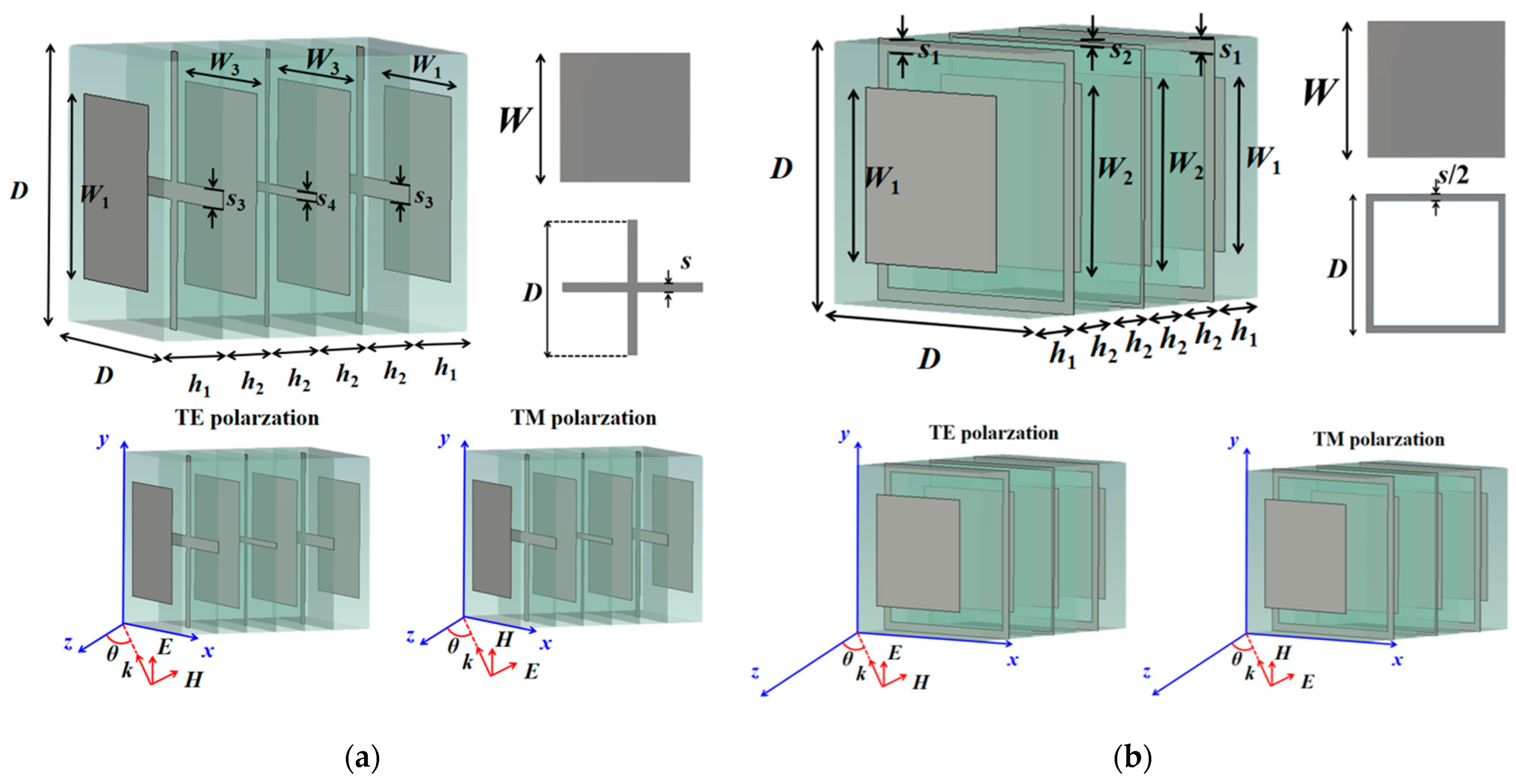
Figure 2.
Equivalent circuit model of traditional miniaturized FSSs.

Figure 3.
Unit cell of design B is placed inside a waveguide with periodic boundary conditions.

Figure 4.
Simulated S-parameter results of (a) design A and (b) design B from the CST.

Figure 5.
Simulated transmission coefficients of traditional miniaturized FSSs under different angles of incidence from the CST. (a,b) Design A under TE and TM polarization; (c,d) design B under TE and TM polarization.
Figure 5.
Simulated transmission coefficients of traditional miniaturized FSSs under different angles of incidence from the CST. (a,b) Design A under TE and TM polarization; (c,d) design B under TE and TM polarization.
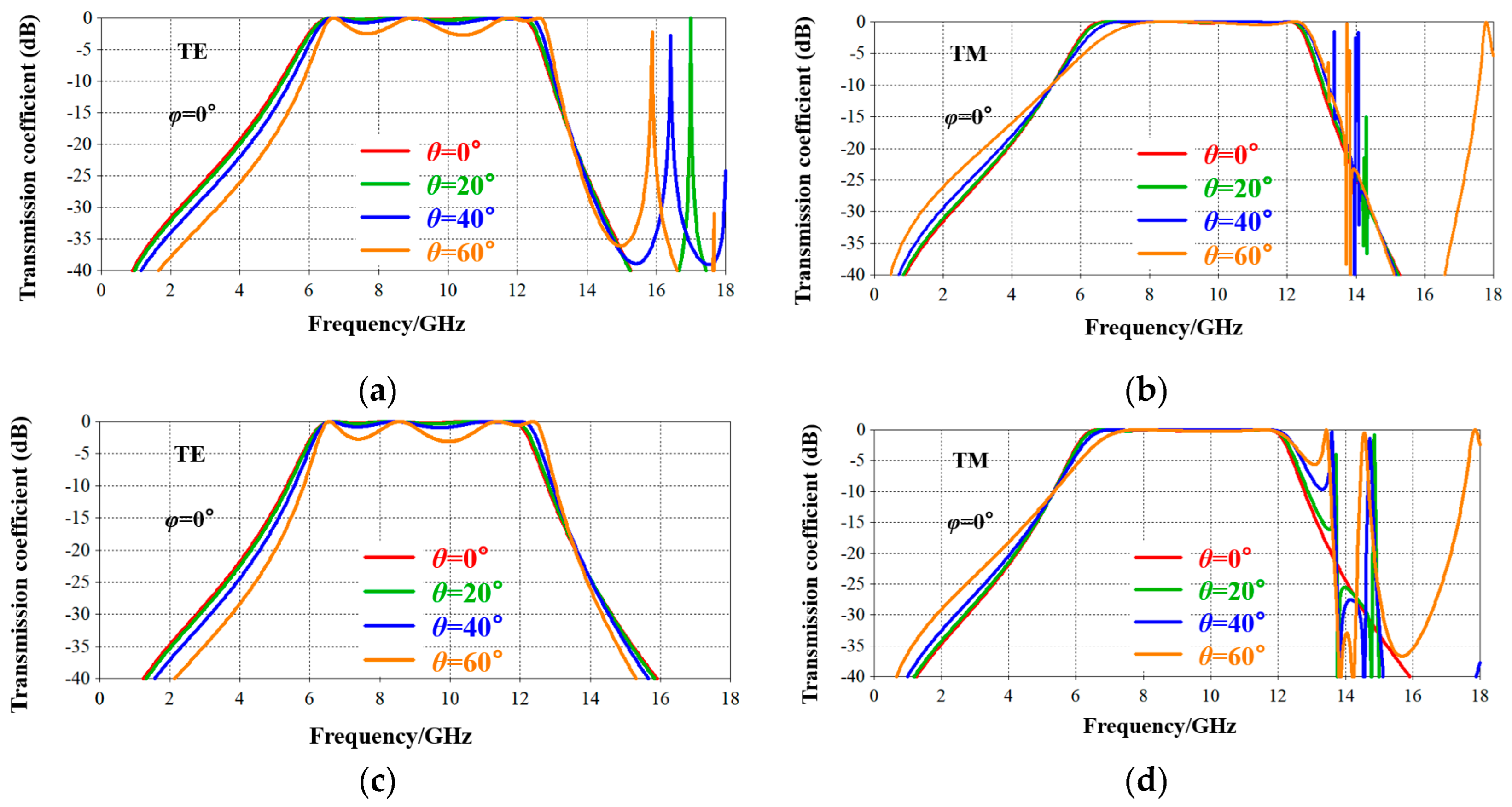
Figure 6.
Current patterns at the different frequencies of transmission zeros. (a) 13.77 GHz; (b) 14.562 GHz; (c) 15.354 GHz.
Figure 6.
Current patterns at the different frequencies of transmission zeros. (a) 13.77 GHz; (b) 14.562 GHz; (c) 15.354 GHz.
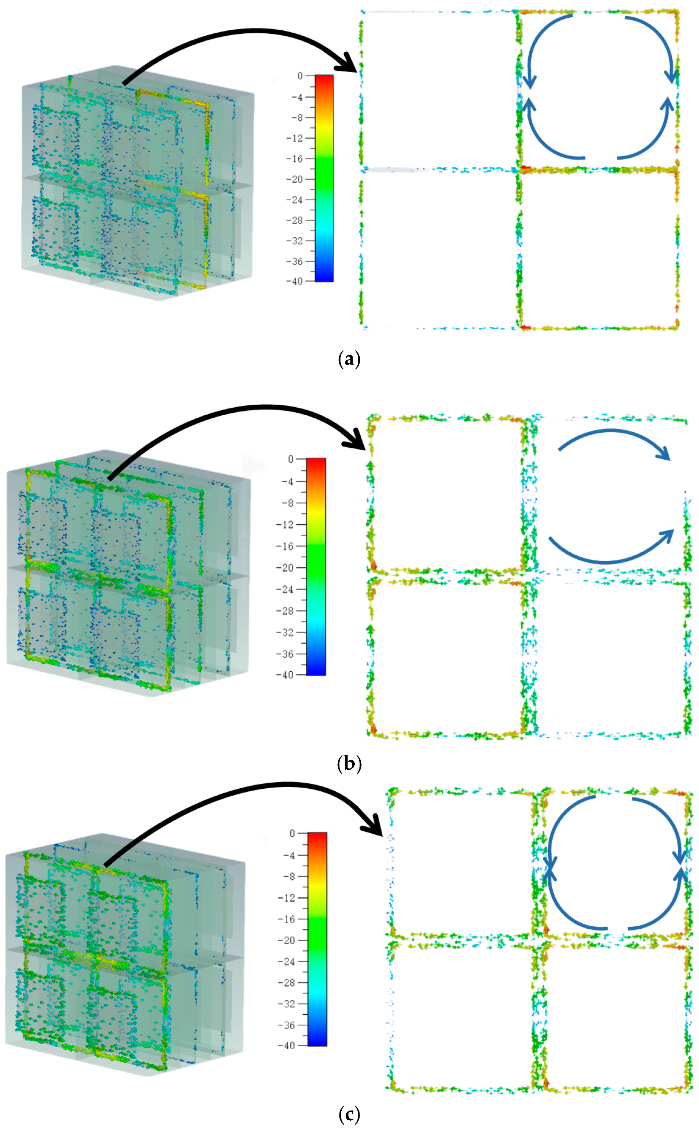
Figure 7.
Comparison of two traditional and modified 2.5-D miniaturized FSSs’ unit cells. (a) Unit of design A; (b) Unit of design B; (c) Modified unit of design A; (d) Modified unit of design B.
Figure 7.
Comparison of two traditional and modified 2.5-D miniaturized FSSs’ unit cells. (a) Unit of design A; (b) Unit of design B; (c) Modified unit of design A; (d) Modified unit of design B.
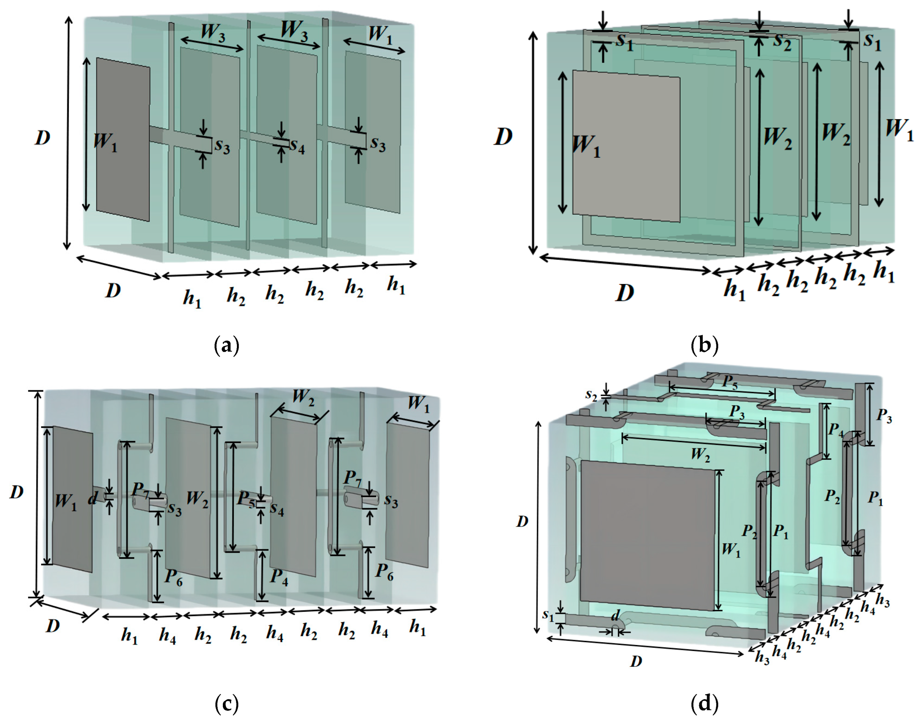
Figure 8.
The equivalent circuit model and the knitted structure of modified design B (the extra inductance Lvia provided by the via is marked in red).
Figure 8.
The equivalent circuit model and the knitted structure of modified design B (the extra inductance Lvia provided by the via is marked in red).

Figure 9.
Simulated S-parameter results of typical FSSs and modified miniaturized FSSs from the CST. (a) Modified design A and design A; (b) modified design B and design B.
Figure 9.
Simulated S-parameter results of typical FSSs and modified miniaturized FSSs from the CST. (a) Modified design A and design A; (b) modified design B and design B.
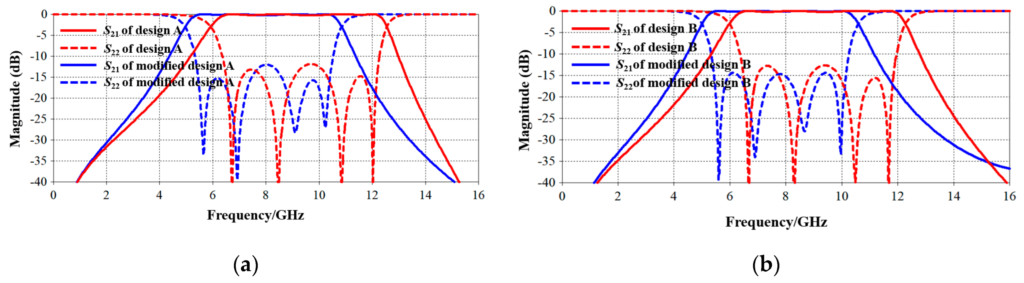
Figure 10.
Simulated transmission coefficients of modified 2.5-D miniaturized FSSs under different angles of incidence from the CST. (a,b) Modified design A under TE and TM polarization; (c,d) modified design B under TE and TM polarization.
Figure 10.
Simulated transmission coefficients of modified 2.5-D miniaturized FSSs under different angles of incidence from the CST. (a,b) Modified design A under TE and TM polarization; (c,d) modified design B under TE and TM polarization.

Figure 11.
Simulated transmission coefficients of traditional and modified 2.5-D miniaturized FSSs in case of 40 deg incident angle under TM polarization from the CST. (a) Transmission coefficients of modified design A and design A; (b) transmission coefficients of modified design B and design B.
Figure 11.
Simulated transmission coefficients of traditional and modified 2.5-D miniaturized FSSs in case of 40 deg incident angle under TM polarization from the CST. (a) Transmission coefficients of modified design A and design A; (b) transmission coefficients of modified design B and design B.

Figure 12.
Photograph of PCB layers of (a) modified design A sample; (b) design A sample.
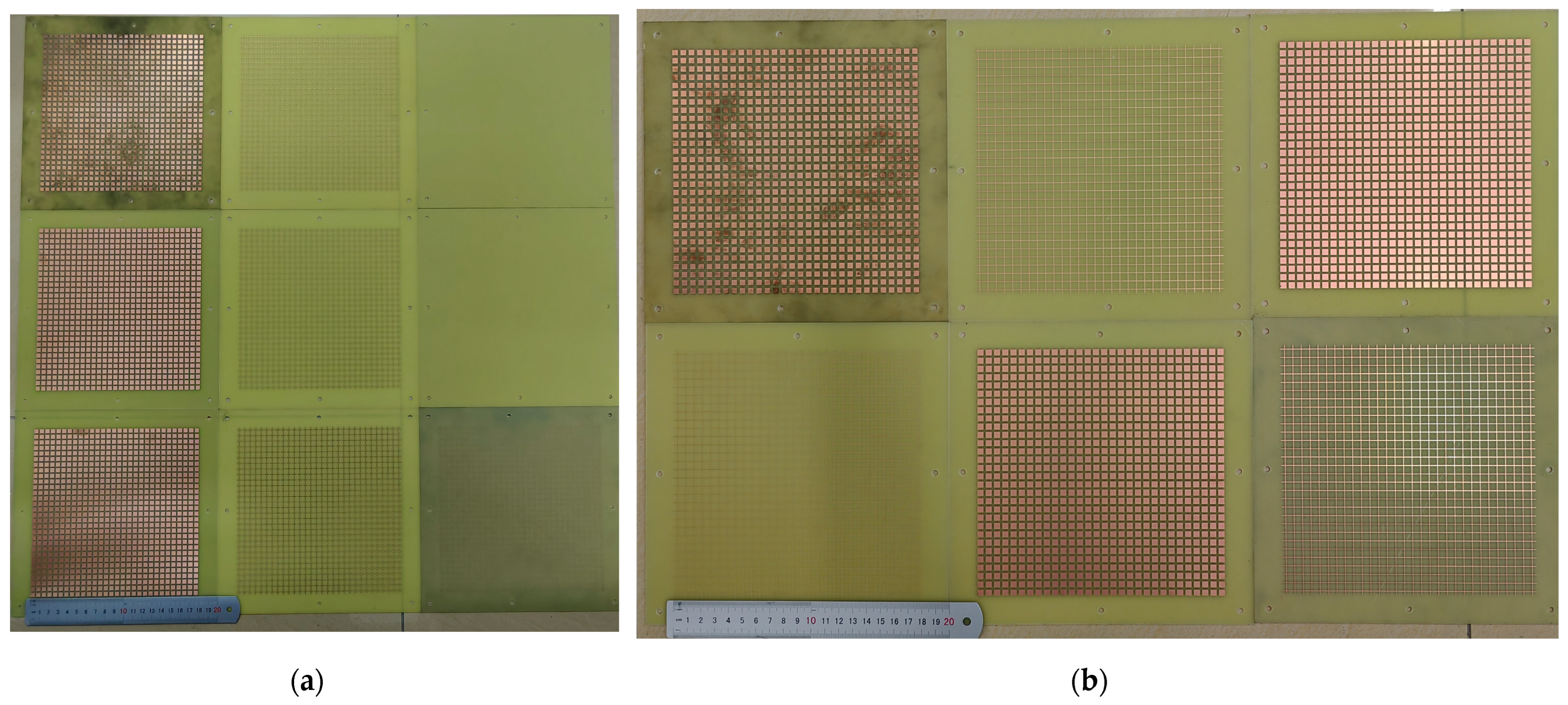
Figure 13.
Photograph of assembled miniaturized FSS samples. (a) Metallic patch layer of modified design A sample; (b) knitted structure layer of modified A sample; (c) metallic patch layer of design A sample; (d) metallic wire frame layer of design A sample.
Figure 13.
Photograph of assembled miniaturized FSS samples. (a) Metallic patch layer of modified design A sample; (b) knitted structure layer of modified A sample; (c) metallic patch layer of design A sample; (d) metallic wire frame layer of design A sample.
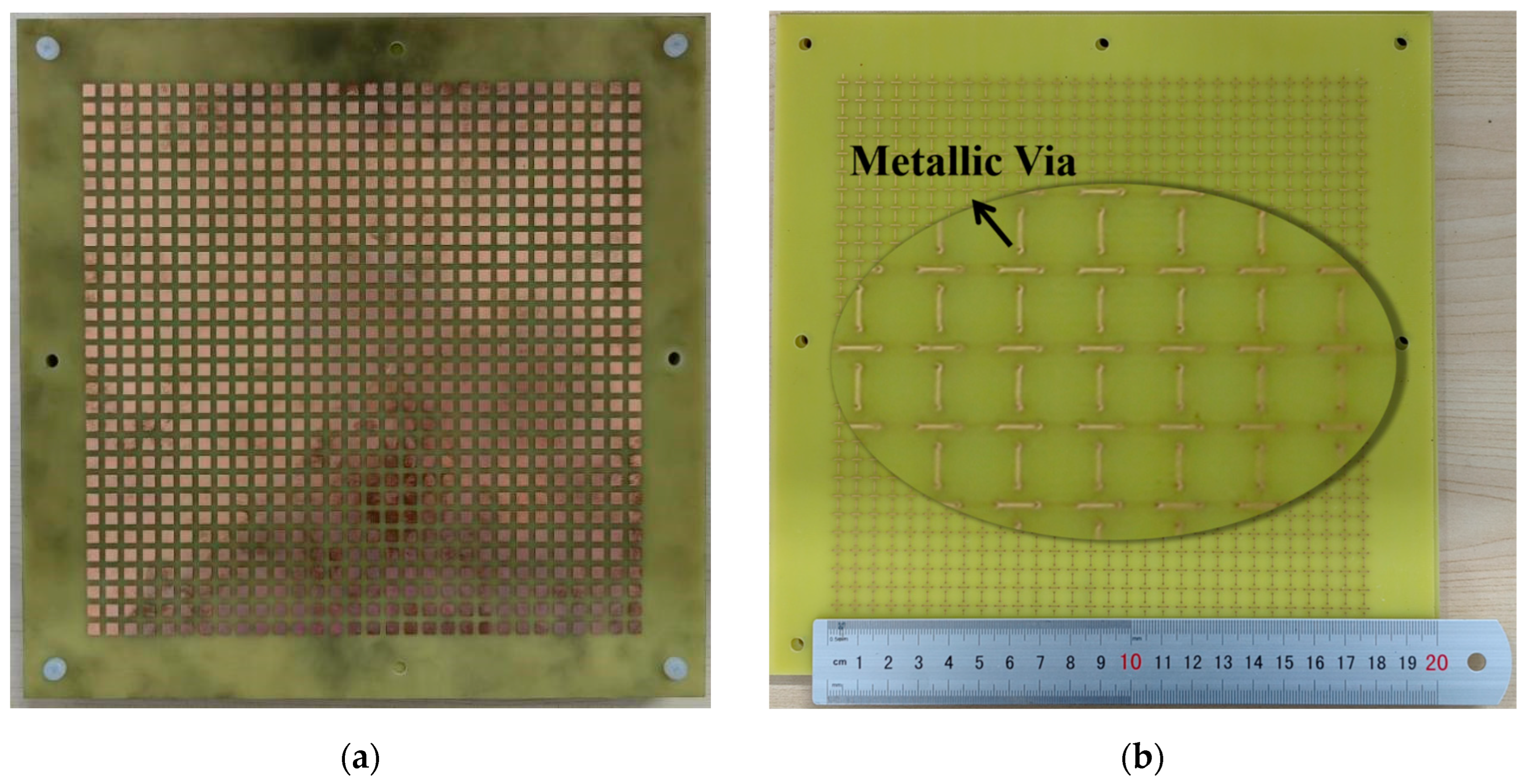
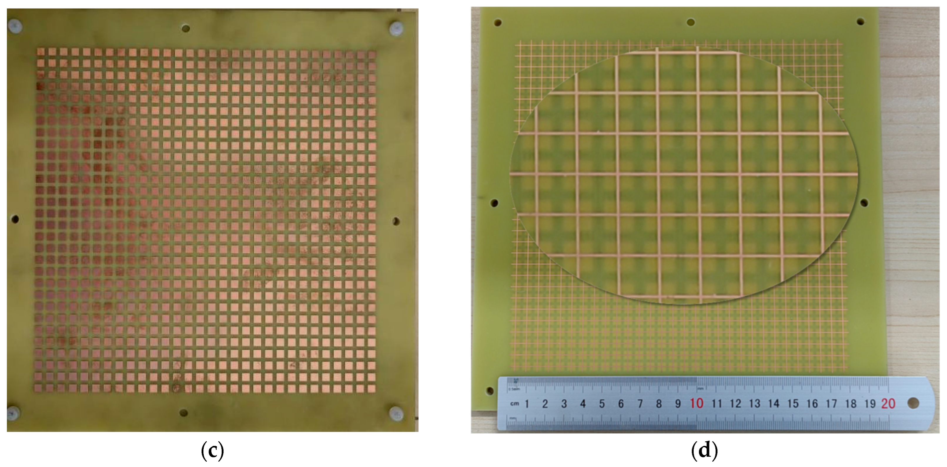
Figure 14.
Photograph of the miniaturized FSS samples and the experimental environment. (a) Modified design A sample; (b) design A sample.
Figure 14.
Photograph of the miniaturized FSS samples and the experimental environment. (a) Modified design A sample; (b) design A sample.
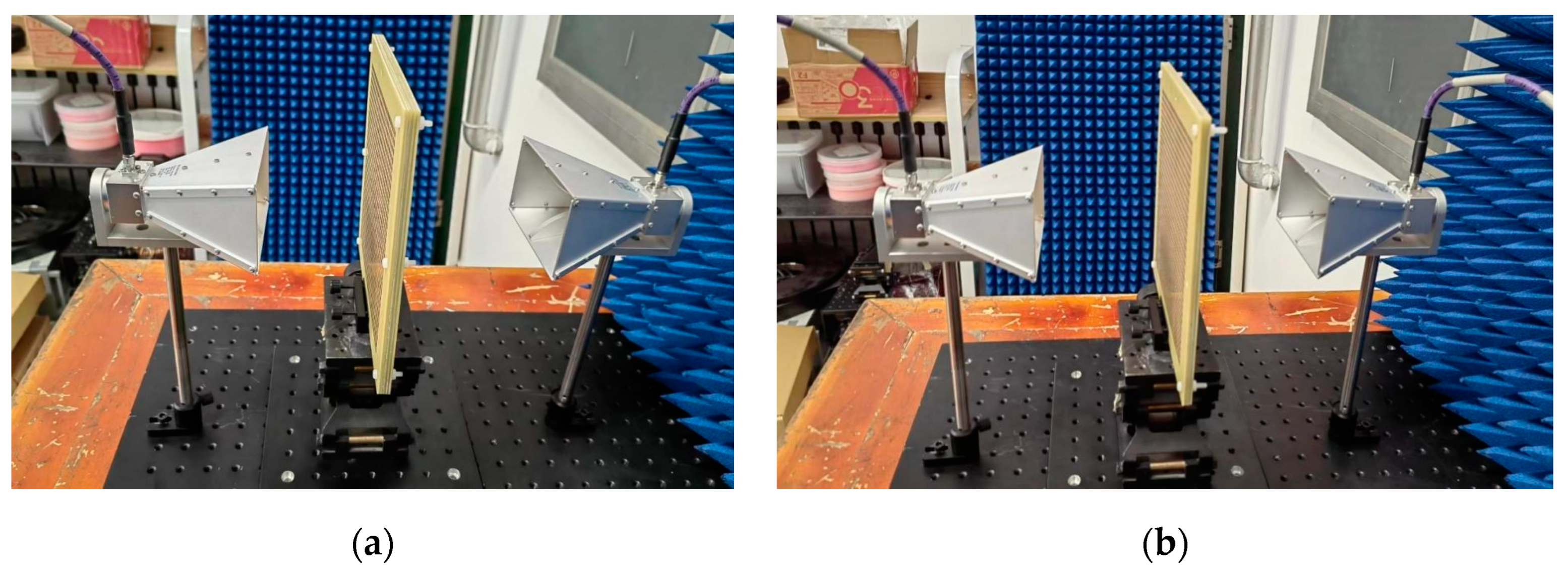
Figure 15.
Measured and simulated results of design A under the various incident angles. (a) TE polarization; (b) TM polarization.
Figure 15.
Measured and simulated results of design A under the various incident angles. (a) TE polarization; (b) TM polarization.

Figure 16.
Measured and simulated results of modified design A under the various incident angles. (a) TE polarization. (b) TM polarization.
Figure 16.
Measured and simulated results of modified design A under the various incident angles. (a) TE polarization. (b) TM polarization.
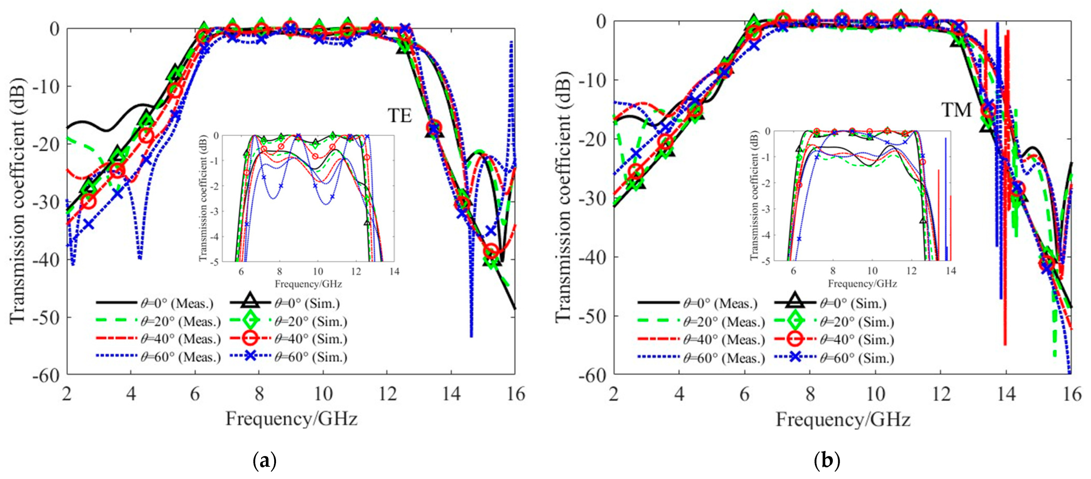
Figure 17.
Comparison of measured results for design A and modified design A under oblique incidence.
Figure 17.
Comparison of measured results for design A and modified design A under oblique incidence.
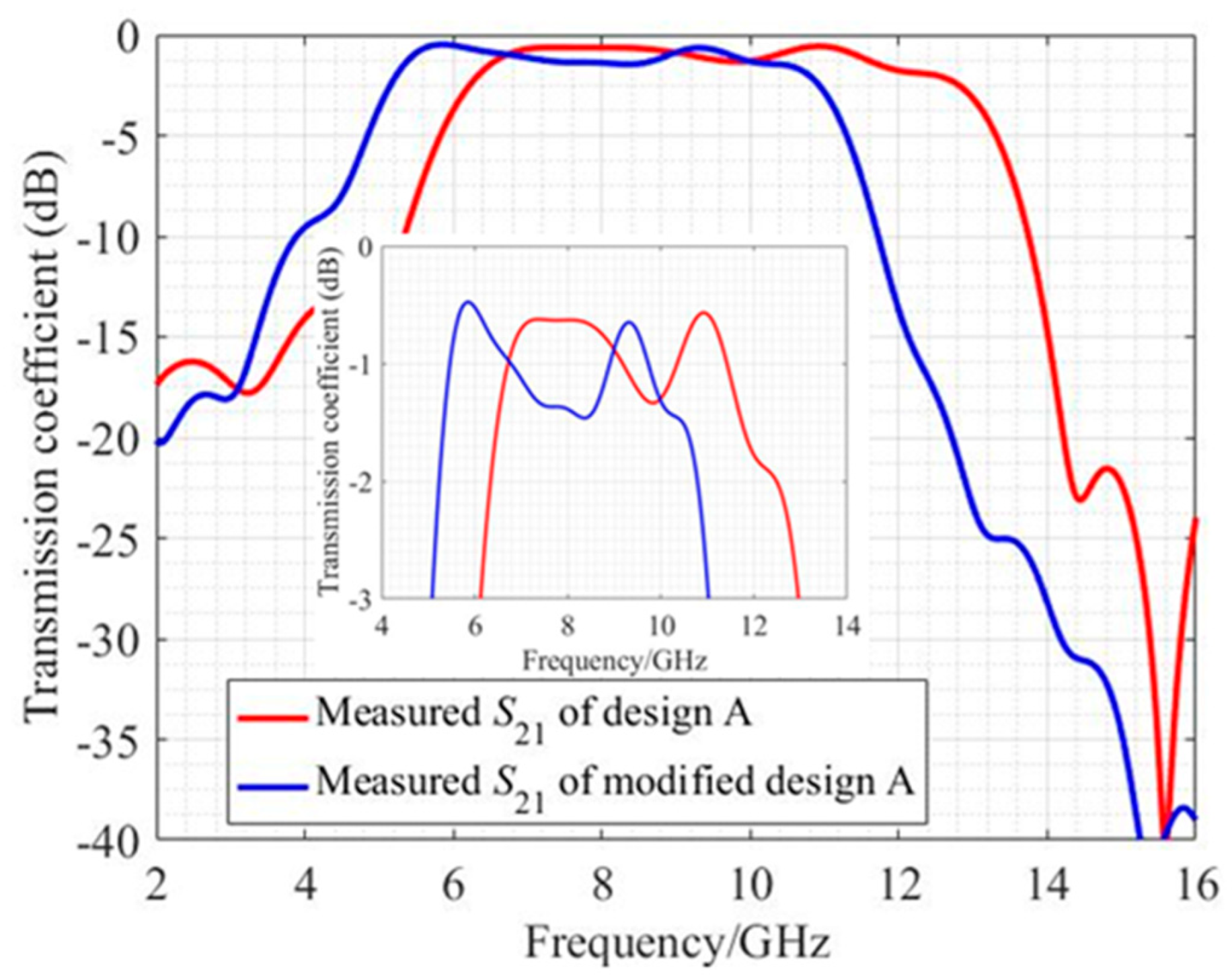
Table 1.
Dimensions of traditional fourth-order miniaturized FSSs.
| Parameters | D | W1 | W2 | W3 | s1 |
| Values | 6 mm | 4 mm | 4.3 mm | 4.4 mm | 0.3 mm |
| Parameters | s2 | s3 | s4 | h1 | h2 |
| Values | 0.1 mm | 0.4 mm | 0.2 mm | 1.5 mm | 1.2 mm |
Table 2.
Dimensions of modified fourth-order miniaturized FSSs.
| Parameters | D | W1 | W2 | W3 | s1 |
| Values | 6 mm | 4 mm | 4.3 mm | 4.4 mm | 0.3 mm |
| Parameters | s2 | s3 | s4 | h1 | h2 |
| Values | 0.1 mm | 0.4 mm | 0.2 mm | 1.5 mm | 1.2 mm |
| Parameters | h3 | h4 | P1 | P2 | P3 |
| Values | 1.4 mm | 1 mm | 3.6 mm | 3 mm | 1.8 mm |
| Parameters | P4 | P5 | P6 | P7 | d |
| Values | 1.6 mm | 3.2 mm | 1.5 mm | 3.4 mm | 0.2 mm |
Disclaimer/Publisher’s Note: The statements, opinions and data contained in all publications are solely those of the individual author(s) and contributor(s) and not of MDPI and/or the editor(s). MDPI and/or the editor(s) disclaim responsibility for any injury to people or property resulting from any ideas, methods, instructions or products referred to in the content. |
© 2024 by the authors. Licensee MDPI, Basel, Switzerland. This article is an open access article distributed under the terms and conditions of the Creative Commons Attribution (CC BY) license (https://creativecommons.org/licenses/by/4.0/).
Share and Cite
MDPI and ACS Style
Zhu, J.; Wang, Q.; Jin, M. High-Order Wideband Band-Pass Miniaturized Frequency-Selective Surface with Enhanced Equivalent Inductance. Electronics 2024, 13, 925. https://doi.org/10.3390/electronics13050925
AMA Style
Zhu J, Wang Q, Jin M. High-Order Wideband Band-Pass Miniaturized Frequency-Selective Surface with Enhanced Equivalent Inductance. Electronics. 2024; 13(5):925. https://doi.org/10.3390/electronics13050925
Chicago/Turabian StyleZhu, Jianjie, Qian Wang, and Ming Jin. 2024. "High-Order Wideband Band-Pass Miniaturized Frequency-Selective Surface with Enhanced Equivalent Inductance" Electronics 13, no. 5: 925. https://doi.org/10.3390/electronics13050925
Note that from the first issue of 2016, this journal uses article numbers instead of page numbers. See further details here.