
Design of a 12-Bit SAR ADC with Calibration Technology

School of Electronics and Information Engineering, South China Normal University, Foshan 528225, China
*
Author to whom correspondence should be addressed.
Electronics 2024, 13(3), 548; https://doi.org/10.3390/electronics13030548
Submission received: 11 December 2023
/
Revised: 21 January 2024
/
Accepted: 25 January 2024
/
Published: 30 January 2024
(This article belongs to the Special Issue Advances in Analog and Mixed-Signal Integrated Circuits)
Abstract
:Successive approximation register (SAR) analog-to-digital converters (ADC) have the advantages of a simple structure, low power consumption and a small area compared with other types of ADCs, and thus, high-performance SAR ADCs have always been a hot research topic in the industry. In this paper, a 12-bit SAR ADC design with calibration using a hybrid RC digital-to-analog converter(RC DAC) structure is proposed to improve the conversion accuracy of the ADC and reduce the circuit area at the same time. The analog supply voltage and reference voltage of the ADC are 3.3 V, and the digital supply voltage is 1.2 V. The ADC adopts a mixed digital–analog design scheme, in which the internal comparator, latch, DAC capacitor array, etc., are analog parts, and the rest of the SAR algorithms and calibration algorithms are all implemented in digital Verilog code, with a conversion accuracy of 0.8 mV and a calibration accuracy of 0.5 LSB. The ADC can be selectively calibrated, and the simulation shows that the accuracy of the calibrated ADC can be guaranteed to be within 2 LSB under a 14 MHz digital clock with a sampling rate of 1 MHz. After simulation at a sampling rate of 1 MHz and an input frequency of 244 Hz sine wave, the effective bit count of the ADC is 9.54 bits and the SFDR is 63.71 dB. The circuit consumes 1.78 mW with a 3.3 V supply voltage. The overall layout core area is 411 m × 517 m.
1. Introduction
As technology advances, the nature of information that people can receive becomes more and more diverse. For example, light, electricity, sound and temperature are continuous analog signals. However, in practical applications, analog signals are usually converted to digital signals and processed [1] because digital signals have the advantages of being easy to process and store, are anti-interference and have high accuracy. In order to realize the mutual conversion between analog and digital signals, analog-to-digital converters (ADCs) have been proposed. An ADC is one of the most important modules in signal processing; its role is to convert analog signals into digital forms so that people can be processed, stored and transmitted digitally. It is a bridge between analog signals and digital signals, and the study of analog-to-digital converters is of very great significance. ADCs are widely used in various fields, including portable electronics, wireless communications, medical device equipment, industrial automation, data signal collectors, military imaging and aerospace, radar sonar detection and control systems and other fields [2].
According to their different operating principles and structures, ADCs can be divided into different types. The current common types of ADCs are flash type, pipeline type, type and successive approximation register (SAR) analog-to-digital converter, but these cannot take into account accuracy, speed, power consumption and other indicators. For example, flash ADCs have the fastest conversion speed, but their power consumption and area are very large; ADCs have the highest accuracy, but are slower; pipelined ADCs can achieve a better compromise between speed and accuracy, but their structure is more complex [3]. In contrast, the SAR ADC studied in this paper can better compromise the relationship between power consumption, speed and accuracy, and because of its simple structure, its low power consumption, and its occupation of an area so small and so high-performance, SAR ADCs have become the industry’s research hot spot [4]. A SAR ADC mainly uses a binary search algorithm to control the capacitor array charging and discharging to approximate the analog input values one by one, and then quantizes them to obtain the corresponding digital code; this approximation adjustment ensures the high accuracy of the conversion results.
In recent years, with the widespread application of digital signal processing technology to electronic systems, higher requirements have been placed on the accuracy of SAR ADCs produced by CMOS processes. The conversion accuracy of SAR ADCs is closely related to the binary weighting ratio between the capacitors in the main DAC [5]. However, this binary weighting is affected by parasitic effects and capacitor mismatch brought about by process manufacturing errors. With the continuous maturity of the process and the adjustability of the layout design, the impact of parasitic effects can be continuously reduced at the design stage [6]. However, due to unavoidable errors in the process, the capacitance value when making the capacitor will produce a certain deviation, resulting in a random mismatch. This capacitance mismatch problem in the SAR ADC circuit greatly limits the accuracy of the ADC [7]. So, calibrating its internal capacitance mismatch is a necessary step to realize a high-precision SAR ADC.
This paper focuses on the design of a 12-bit SAR ADC with a calibration technique, which is adopted in addition to the quantization of the main DAC and the addition of a secondary DAC circuit for calibration, which is used to calibrate the main DAC capacitance mismatch to achieve the calibration so as to improve the conversion accuracy of the SAR ADC. At the same time, the DAC capacitance array uses a mixture of a low 4-bit resistor and a high 8-bit capacitor in the resistive–capacitive DAC. This can greatly reduce the area of the layout. The main content of this paper contains the overall circuit design of this ADC, the calibration principle and procedure of the circuit and the analysis of the simulation results.
2. SAR ADC Overall Circuit Design
2.1. Overall Circuit Structure
The overall circuit structure of the SAR ADC proposed in this paper is shown in Figure 1.
The overall circuit can be divided into analog and digital parts and contains comparator circuits, latch circuits, switching circuits, level shifting circuits, DAC capacitor arrays, digital SAR and digital calibration circuits. The switches in the analog section of the ADC are controlled by digital successive approximation logic and digital calibration circuitry used to accomplish the successive approximation logic and to calibrate the ADC for capacitive mismatches. The digital circuit is a gate-level circuit synthesized from Verilog code, which is supplied with a voltage of 1.2 V, while the analog circuit is supplied with a voltage of 3.3 V, so it is necessary to perform a level conversion at the interface between digital and analog.
2.2. DAC Circuit Design
Capacitor arrays are one of the centerpieces of SAR ADCs [8]. Since the number of capacitors in conventional DAC capacitor arrays grows exponentially with increasing accuracy, which may lead to an increase in layout area as well as an increase in power consumption, it is necessary to reduce the number of capacitors in capacitor arrays in practical designs. Therefore, for hybrid RC DAC arrays, the resolution ratio of capacitance to resistance is particularly important. From the point of view of area minimization, equal resolution segmentation is the best solution. Due to the different unit areas of resistors and capacitors, the optimal ratio of segmented resolution is shifted in hybrid DAC structures [9]. Therefore, the literature [9] provides the following formula for the optimal number of resolution bits with respect to K:
N is a resolution of DAC, K is a resolution of capacitive segment and m is a segment’s area ratio (resistor area/capacitor area).
After calculation, the optimal value of K is taken as 6 when only area minimization is considered, but since resistors are more susceptible to component mismatch than capacitors, if the resolution of the resistive segment is taken to be on the large side, the performance of the whole ADC will be affected. So, after the above compromise, K is taken as 8, i.e., the DAC capacitor array consists of a hybrid RC-DAC with a low 4-bit resistor and a high 8-bit capacitor, and the advantage of this structure is that it overcomes the traditional SAR ADC’s capacitor array size requirements and can greatly reduce the circuit area [10]. The DAC capacitance array contains a capacitance main DAC circuit, a capacitance calibration sub-DAC circuit, and a resistor divider DAC circuit, and the capacitance calibration sub-DAC circuit can calibrate the capacitance mismatch generated by the calibration capacitance main DAC circuit. Since the circuit contains a self-calibration structure, it is able to calibrate the mismatch of the comparator inside the circuit before the analog-to-digital conversion [11], and it is able to output the mismatch in the form of a calibration code so that the value of the mismatch inside the converter is known. The working process of this structure is divided into two stages: the calibration stage and the analog-to-digital conversion stage [12].
2.3. Comparator and Latch Design
The comparator and latch circuits used in this paper are shown in Figure 2. The comparator is used to compare the difference between the upper plate voltage outputs of the capacitors in the capacitor main DAC circuit and the capacitor calibration sub-DAC circuit, and then the result of the comparison is sent to the latch for locking. After the locking is completed, the result of the locking is sent to the digital SAR and digital calibration circuits for processing.
The comparator is a critical part of the successive approximation analog-to-digital converter circuit, and the accuracy of the comparator is affected by the input misalignment. In the CMOS standard process, the out-of-tune voltage is a random quantity, which can have a great impact on the performance of the comparator and thus seriously affect the accuracy of the comparator. To improve the accuracy of the analog-to-digital converter, it is necessary to calibrate the comparator for misalignment. So, this paper adopts the output misalignment calibration technique. First, ST is set to 0; at this time, the positive and negative inputs of the comparator and one end of the capacitors and are shorted to the common mode level so that the comparator’s out-of-phase voltage is saved to the output coupling capacitance and . And then, when the signal is inputted, the charge stored on capacitance and will be compensated for the out-of-phase voltage, and the comparator’s out-of-phase calibration operation will also be completed.
3. Calibration Principles and Processes
3.1. Calibration Principle
Due to the deviation of the process, the capacitance value when the capacitor is made will cause a certain deviation, resulting in a random mismatch, which in turn will cause the accuracy of the ADC to decrease, so it is necessary to calibrate the capacitance mismatch of the ADC. The basic principle of calibration is to quantify the mismatch error of the capacitor through the capacitance calibration sub-DAC circuit, record the amount of error in the register, and when the conversion is formally started, the amount of error is canceled out in the process of approximation so as to achieve the purpose of calibration.
The following is an example of calibrating the error of the ith-bit capacitor in a capacitor array. Let the capacitance error ratio of the ith-bit capacitor be ; then, the value of this capacitor can be expressed as in Equation (2):
The amount of error in the capacitor is converted to the voltage corresponding to it, and the amount of voltage error due to the mismatch of the ith capacitor is noted as .
As shown in Figure 3, if you need to calibrate the ith-bit capacitor, first connect all the upper plates of all capacitors to the common-mode level , the lower plates of capacitors smaller than the ith-bit are connected to the end, and the lower plates of the rest of the capacitors are connected to ground. At this time, the charge of the upper plate Q is
Then, the upper pole plate of the capacitor is disconnected from , the lower pole plate of the ith position capacitor is connected to the reference voltage terminal and the lower pole plate of the capacitor lower than is switched to the ground potential. Let the voltage value of the upper pole plate of all capacitors at this time be , which is known by the law of conservation of charge:
The collation gives the value of the voltage at the upper pole plate of all capacitors at this point:
This gives the voltage difference between and the low capacitance sum. Equation (6) is obtained when considering the case :
In general, , but since there is an error, the actual value of the capacitance is , which is obtained as
where , that is, the amount of mismatch brought about by the amount of error is recorded as . The use of the capacitance-calibrated sub-DAC circuit will be quantized out of the value of the voltage quantization of the highest capacitance in the second after dividing by two to obtain the value of the highest capacitance quantization of the amount of . This value is stored in a register in the ADC data conversion and will be taken out of the register from the value of the switching module of the ADC-calibrated sub-DAC circuit to remove the first N for the capacitance of the mismatch of error brought about by the module.
For the capacitance of the ith position, the error amount with its lower capacitance sum can also be obtained by a similar approach; however, cannot directly correspond to the ith position error amount, and its error amount is also related to the capacitance error amount of the higher position. It can be expressed using the relation
The error amount of each capacitor obtained is saved into the register, and when the ith bit is set to 1 during the formal conversion, is taken out of the register and put into the error accumulation register, and then it is judged by the comparator. If the output value of the comparator is 1, it means that the value needs to be accumulated, and if the output is 0, it means that the value does not need to be accumulated, and it is cleared out from the error register.
3.2. Calibration Process
3.2.1. Calibration Sampling Stage
To calibrate the capacitance of the highest bit, for example, first connect the capacitance of the highest bit to , the remaining capacitance to , the positive and negative inputs of the comparator are shorted to the common-mode level of , and the value of the switch SC[6:0] is preset to to complete the calibration sampling process.
3.2.2. Calibration Conversion Stage
To calibrate the conversion, first connect the highest capacitor to and the remaining capacitor to , with the positive and negative inputs of the comparator suspended. Through the digital SAR and digital calibration circuit control, switch SC[6:0], and then, adjust the capacitance calibration sub-DAC circuit capacitor voltage on the pole plate so that it is constantly approaching the voltage of the positive end of the comparator to quantify the error voltage due to the capacitance mismatch brought about. The value of SC[6:0] obtained after the calibration of each mismatch capacitor is , and the error of this bit on the low capacitance is
The amount of error in the ith-bit capacitor is obtained as
During the conversion process, there is an error accumulation register that accumulates the value corresponding to the previous bit that was reserved as 1 during the analog-to-digital conversion. After accumulation, the value Y of the error accumulation register is added to and output to SC[6:0] for calibration. Since the lower four bits of the ADC consist of resistors, only the upper eight bits are calibrated for capacitance here.
The flowchart for performing a calibration is shown in Figure 4. Since the error in the last four bits of the calibration is the same as that in the fifth bit, the minimum value of i in the flowchart is 4. When 12 calibrations have been completed, the value of Y in the error accumulation register described above is obtained:
3.3. Analog-to-Digital Conversion
After calibration is complete, the ADC begins normal analog-to-digital conversion, which is again divided into two stages: sampling and conversion. When the ADC samples the input signal, all capacitors in the capacitor main DAC array are connected to the analog input , the lower plate is connected to the common-mode level , and the value of SC[6:0] is . At this time, the charge of the upper plate of all capacitors in the capacitor main DAC circuit is
When the data begin to be converted, each switch state is shown as in Figure 5. At this time, the positive and negative inputs of the comparator are disconnected from , and the highest bit (MSB) of D[11:0] is first set to 1, and all other bits are set to 0. At this time, the charge on all capacitors at the main DAC circuit end of the capacitor is
is the lower plate voltage at the main DAC circuit end of the capacitor. By conservation of the charge,
When the capacitor mismatch is not considered, there is no change in the switch at the negative input of the comparator, so the voltage at the negative input of the comparator is unchanged:
So, it follows that
and calibrated input comparator are used for comparison: if the comparator output is 1, then D[11] is kept as 1, D[10] is changed from 0 to 1, and the other bits are kept as 0, and vice versa, if D[11] is changed to 0, D[10] is changed from 0 to 1, and the other bits are unchanged, and so on. After 12 conversion cycles of successive approximations, the final ADC analog-to-digital conversion is completed once the conversion cycle is completed.
4. Simulation Results
4.1. Error Analysis
In order to build the circuit according to the above structure, to simulate the circuit in the Cadence environment using Spectre, and to test the actual output and the theoretical output values of the error, this paper also uses Verilog at the same time to build a 12-bit ADC in the ideal case, using the same sampling data in the ideal ADC and the calibrated actual ADC, and gives the results of the simulation for comparison.
As shown in Figure 6, a sine wave with input frequencies of 200 Hz and 1 KHz is fed into the ideal ADC and the actual ADC, respectively, and the output conversion values are compared.
From Figure 6, it can be seen that, in the case where there is a mismatch in the ADC capacitance, the calibrated error is within 2 LSB as long as the mismatch value is within the range that can be calibrated. However, due to the different sampling strategies of the ideal ADC and the actual ADC, an error of 3 LSB occurs.
Table 1 compares the digital code with a mismatch and no calibration at the time of the mismatch, the digital code obtained after using the calibration technique at the time of the mismatch and the correct digital code. From Table 1, we can see that when no calibration technique is used during a capacitor mismatch, the error is within 7 LSB. After calibration, the error is controlled within 2 LSB. Therefore, it can be seen that this calibration technique has a good calibration effect on capacitor mismatch.
The following PVT simulation is performed as shown in Figure 7, which shows the error value of the output of the analog-to-digital converter at different temperatures as well as at different process corners for different voltage values input to the analog-to-digital converter for analog-to-digital conversion. Figure 8 shows the error value for a fixed input of 0.5 V to the ADC at different supply voltages, where VDDB denotes the digital supply voltage and VDDA denotes the analog supply voltage.
From the analysis of Figure 7, it can be seen that under different temperature and process angle conditions, different voltage values are input to the ADC, and the errors between the outputs are all within 1 LSB, indicating that the ADC performs well under these conditions. (In Figure 7, the tt process corner error curves coincide with the ss process corner error curves at the test temperatures of −40 °C and 27 °C, and the tt process corner error curves coincide with the ff process corner error curves at the test temperature of 125 °C.)
Figure 8 shows the simulation results based on the same input voltage at varying temperatures, process angles and supply voltages, and it can be seen that the error can be controlled within 2 LSB at tt and ff process corners.
4.2. Spectral Analysis
Assuming that the input 200 Hz sine wave is sampled at a sampling rate of 1 MHz, there are 4096 sampling points, but to satisfy the coherent sampling theorem, the frequency of the input sinusoid is finally taken to be 244 Hz. The output is then spectrally analyzed, and the spectrum analysis and dynamic simulation parameters of the SAR ADC are shown in Figure 9. The ENOB is 9.54 bits and the SFDR is 63.71 dB.
In order to verify the effect of the input frequency on the performance of the ADC and also to satisfy coherent sampling, we input frequencies of 1000 Hz, 1500 Hz and 2000 Hz to the ADC. The final input frequencies are 732 Hz, 1220 Hz and 1708 Hz, respectively, and the comparison of the dynamic characteristic parameters obtained under the simulation of different parameters is shown in Figure 10.
According to the theory, we know that THD will be degraded with the increase in frequency due to nonlinear reasons, so ENOB will also decrease with the increase in frequency. The analog characteristics at different input frequencies are compared in Figure 10, and it can be seen that both SFDR and SNDR (SNR and SNDR approximate overlap)decrease with increasing frequency, while ENOB decreases from 9.54 bit to 7.79 bit. Therefore, the ADC designed in this paper also satisfies this conclusion.
Table 2 shows the comparison between the research papers on 12-bit SAR ADCs in recent years and the data related to this paper.
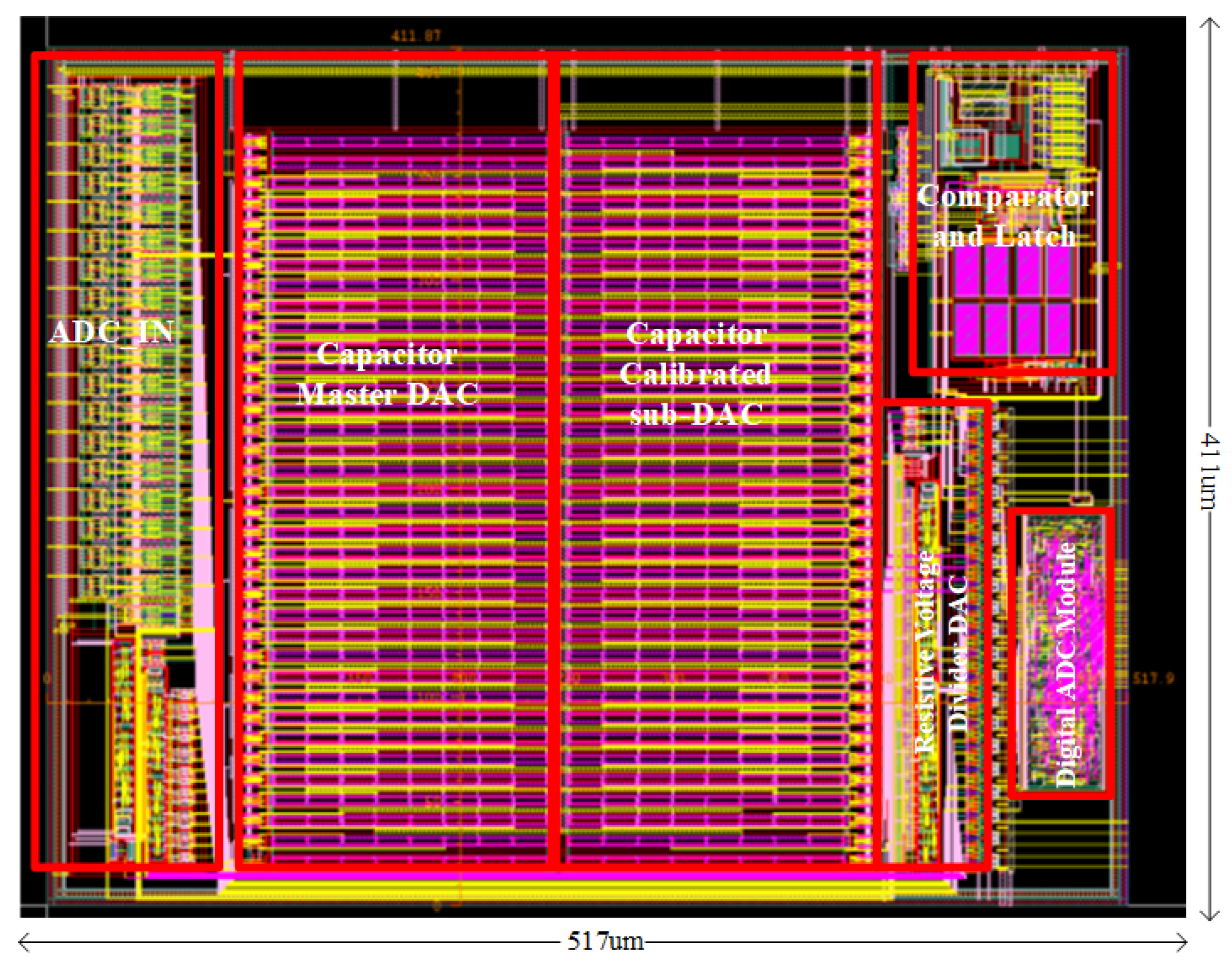
Finally, the ADC layout is shown in Figure 11. The overall layout area is 411 m × 517 m. Although the effective number of bits of this ADC is slightly lower than other ADCs of the same type, the core area is smaller than most ADCs of the same type (e.g., [3,16,17] and those in Table 2), and the layout area of this ADC is smaller than most ADCs of the same type.
5. Conclusions
In this paper, a 12-bit SAR ADC with a calibration technique is designed that utilizes a mixed resistive–capacitive DAC structure of a low 4-bit resistor and a high 8-bit capacitor to reduce the size of the capacitive array, and finally obtains a core area of the chip of about 0.21 mm2, which is small compared to many ADCs of the same type. In addition, as well as the primary DAC used for quantization, a secondary DAC circuit for calibration is additionally added to calibrate the primary DAC for capacitive mismatch to achieve calibration. The method is able to accurately eliminate the mismatch and, at the same time, is able to present the mismatch in the form of a calibration code. Simulations show that, in the presence of the ADC capacitance mismatch, as long as the mismatch value is within the range that can be calibrated, the calibrated error is within 2 LSB. The effective bit count of the simulation is 9.54 bits, and the simulation test results show that this SAR ADC has good performance.
Author Contributions
Conceptualization, D.W.; Funding acquisition, D.W.; Investigation, J.H.; Methodology, D.W. and J.H.; Project administration, D.W.; Resources, Q.Z.; Supervision, X.H.; Validation, D.W. and J.H.; Visualization, J.H.; Writing—original draft, J.H.; Writing—review and editing, D.W. All authors have read and agreed to the published version of the manuscript.
Funding
This work was supported in part by the National Key Research and Development Program of China under grant 2021ZD0114600, in part by the Key-Area Research and Development Program of Guangdong Province under grant 2019B010142002 and grant 2021B1101270004, and in part by the “Special Support Plan” for Top Young Talents in Science and Technology Innovation of Guangdong Province under grant 2021TQ06X978.
Data Availability Statement
Most data are contained within the article. All the data are available on request, subject to restrictions, e.g., privacy or ethics.
Acknowledgments
The authors are grateful to all colleagues and institutions that contributed to this research and made it possible to publish its results.
Conflicts of Interest
The authors declare no conflicts of interest.
References
- Jing, W. Research and Design of a 12-Bit Low Power SAR ADC. Master’s Thesis, Nanjing University of Posts, Nanjing, China, 2021. [Google Scholar] [CrossRef]
- Jinghui, L.; Rensheng, S.; Ruitong, X. Design of 14-bit SAR ADC based on digital self-calibration. China Integr. Circuit 2023, 32, 30–36. [Google Scholar]
- Shuirong, J.; Tianyao, W.; Zhangming, Z. The Key Design Techniques of 12-Bits SAR ADC. Chin. J. Electron Devices 2015, 38, 1022–1030. [Google Scholar]
- Chen, L.; Ma, J.; Sun, N. Capacitor mismatch calibration for SAR ADCs based on comparator metastability detection. In Proceedings of the 2014 IEEE International Symposium on Circuits and Systems (ISCAS), Melbourn, VIC, Canada, 1–5 June 2014; pp. 2357–2360. [Google Scholar]
- Xu, L.; Dai, Z.; Xie, L.; Jin, X. A 12 bit 1 MS/s SAR ADC with Digital self-calibration. Microelectronics 2019, 49, 320–325. [Google Scholar] [CrossRef]
- Wei, L.; Shangshang, G.; Xiao, W.; Shiguang, S. A digital foreground calibration algorithm for SAR ADC. J. Xian Univ. Post Telecommun. 2021, 26, 34–41. [Google Scholar] [CrossRef]
- Yutong, Z.; Xian, G.; Zhe, M. Research and Application of Calibration Technique for Successive Approximation ADC. China Integr. Circ. 2019, 28, 70–75. [Google Scholar]
- Pengzhan, J.; Sheng, D.; Wei, H.; Zhangming, Z.; Shuirong, J. Design and calibration algorithm of high-precision SAR ADC Capacitor Array. Semicond. Technol. 2023, 48, 1020–1029. [Google Scholar] [CrossRef]
- Yenuchenko, M.S.; Kvashina, N.V. Influence Analysis of Mismatch on Nonlinearity in Hybrid RC-DACs. In Proceedings of the 2023 IEEE 24th International Conference of Young Professionals in Electron Devices and Materials (EDM), Novosibirsk, Russia, 29 June–3 July 2023; pp. 400–403. [Google Scholar] [CrossRef]
- Lee, H.S.; Hodges, D. Self-calibration technique for A/D converters. IEEE Trans. Circuits Syst. 1983, 30, 188–190. [Google Scholar]
- Xujun, L.; Rui, L.; Chaofeng, Z.; Huan, D. A digital calibration algorithm for differential structure SAR ADC. China Integr. Circuit 2022, 31, 25–31+65. [Google Scholar]
- Weiming, X.; Jinping, Z.; Li, L. A design of self-calibration 12-bit SAR-ADC. Electron. Packag. 2019, 19, 20–23. [Google Scholar] [CrossRef]
- Li, Z.; Xi, J.; He, L.; Sun, K. A front-end circuit with 16-channel 12-bit 100-kSps RC-hybrid SAR ADC for industrial monitoring application. In Proceedings of the 2016 IEEE Asia Pacific Conference on Circuits and Systems (APCCAS), Jeju, Republic of Korea, 25–28 October 2016; pp. 340–343. [Google Scholar] [CrossRef]
- Lee, J.H.; Lee, K.Y. A Design of Low-Power Bootstrapped CMOS Switch for 20MS/s 12-bit Charge Sharing SAR ADCs. In Proceedings of the 2021 18th International SoC Design Conference (ISOCC), Jeju, Republic of Korea, 6–9 October 2021; pp. 5–6. [Google Scholar] [CrossRef]
- Zhang, J.; Guo, Z.; Li, L.; Xu, R. A Low-Power High-Precision 12Bit SAR ADC. In Proceedings of the 2022 7th International Conference on Integrated Circuits and Microsystems (ICICM), Xi’an, China, 28–31 October 2022; pp. 516–520. [Google Scholar] [CrossRef]
- Qi-zhang, L.; Zhe-ying, L. A Design of a 12-bit 1MSPs SAR ADC. J. Beijing Union Univ. Nat. Sci. 2011, 25, 6–9. [Google Scholar] [CrossRef]
- Kim, M.R.; Kim, Y.O.; Kwak, Y.S.; Ahn, G.C. A 12-bit 200-kS/s SAR ADC with hybrid RC DAC. In Proceedings of the 2014 IEEE Asia Pacific Conference on Circuits and Systems (APCCAS), Ishigaki Island, Japan, 17–20 November 2014; pp. 185–188. [Google Scholar] [CrossRef]
Figure 1.
SAR ADC overall circuit design.

Figure 2.
Comparator and latch structures.

Figure 3.
Calibration of the ith-bit capacitor.
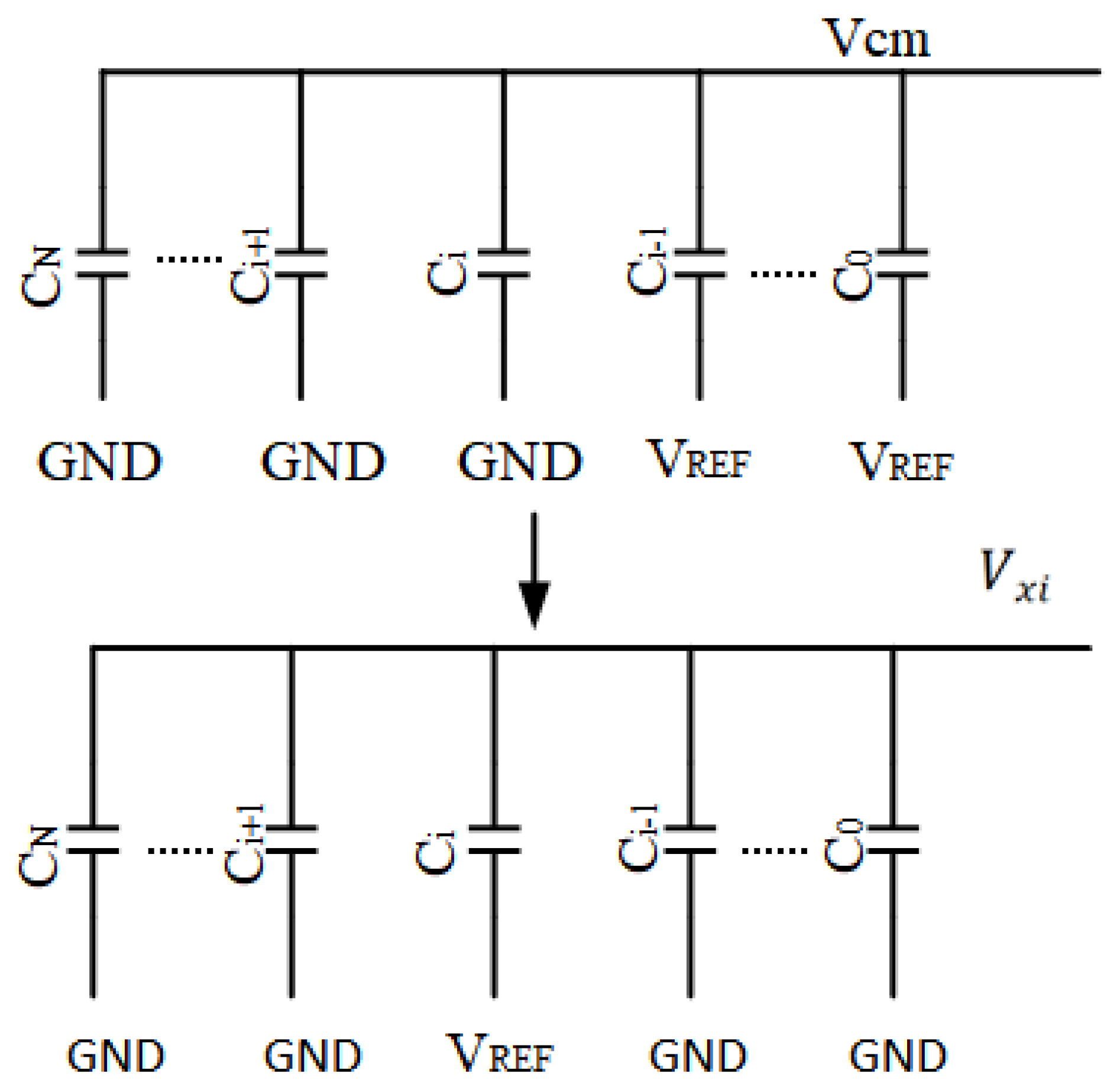
Figure 4.
Flowchart for calibrating the capacitance of a bit.
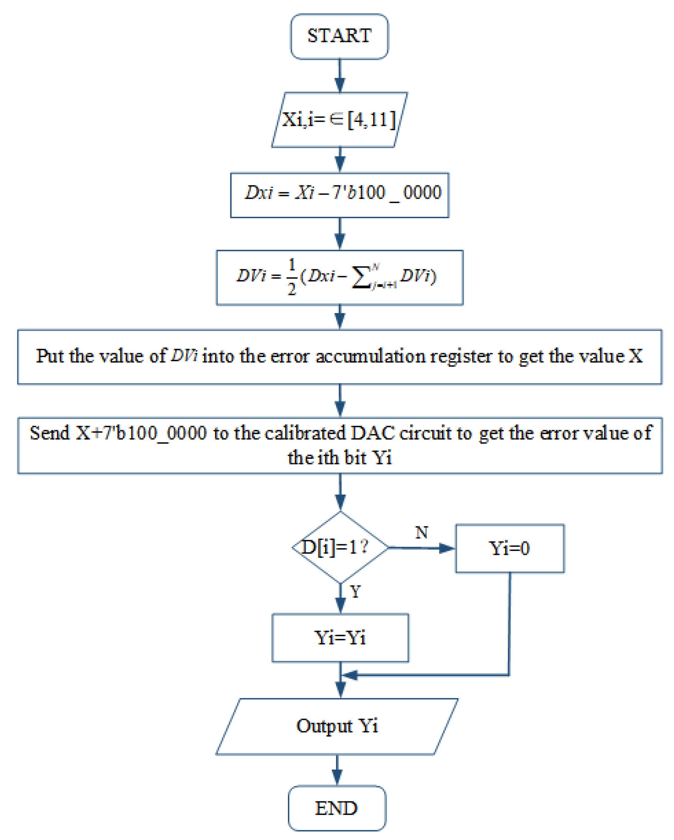
Figure 5.
Status of each switch during digital-to-analog conversion.

Figure 6.
Conversion value error between actual ADC and ideal ADC after simulation.
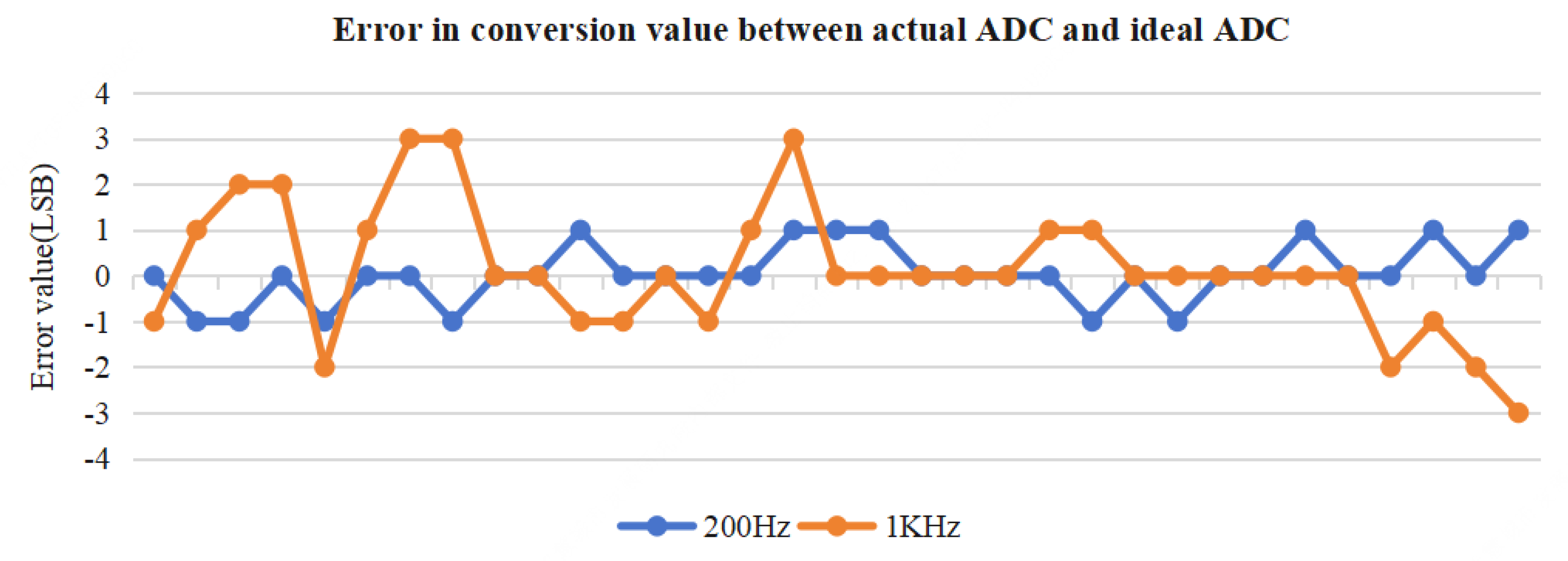
Figure 7.
Conversion error values for the same supply voltage at different temperatures, processing corners and input voltages.
Figure 7.
Conversion error values for the same supply voltage at different temperatures, processing corners and input voltages.

Figure 8.
Conversion error values for the same input voltage at different temperatures, processing angles and supply voltages.
Figure 8.
Conversion error values for the same input voltage at different temperatures, processing angles and supply voltages.

Figure 9.
Spectrum analysis at an input frequency of 244 Hz.
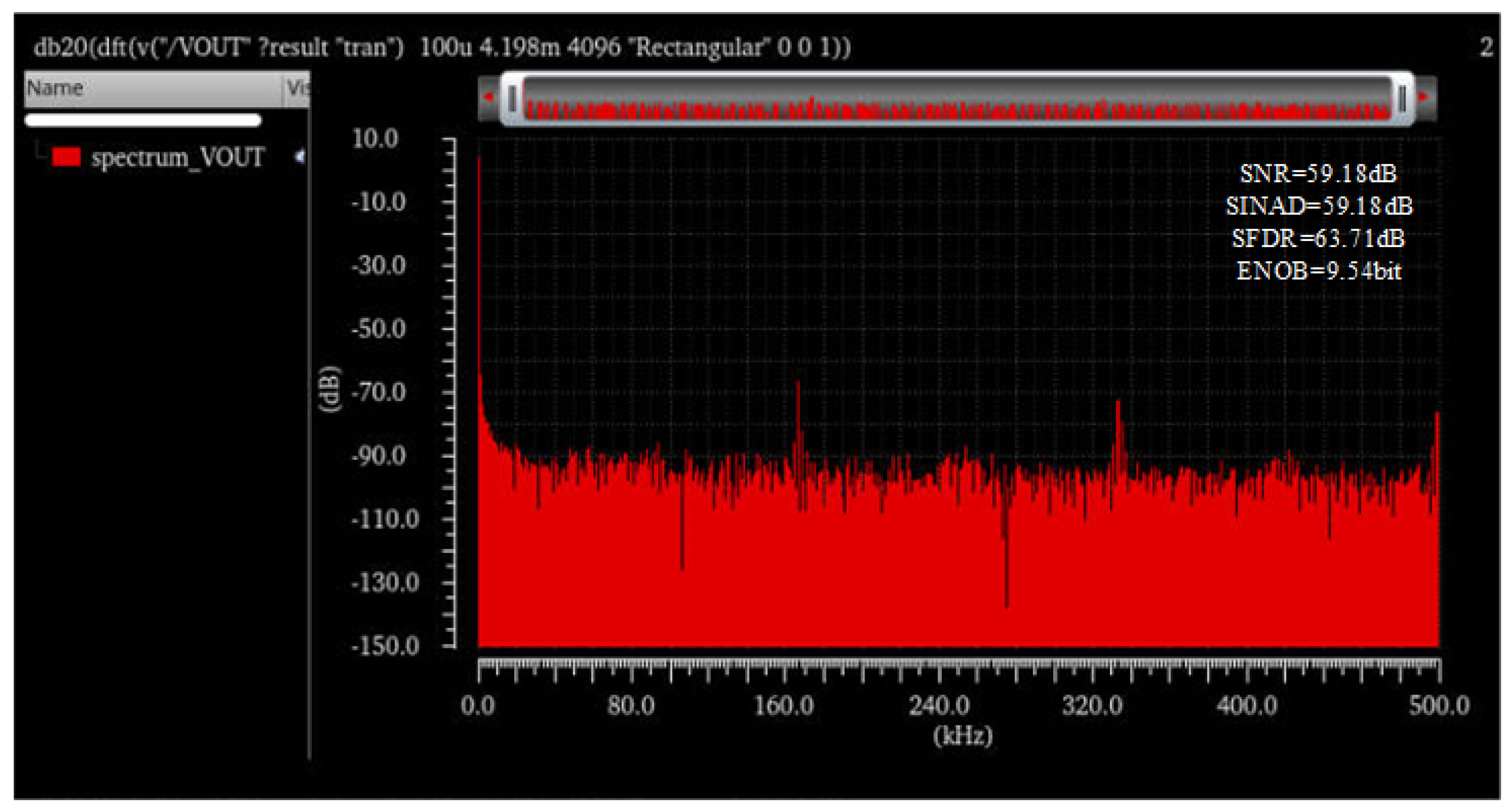
Figure 10.
Dynamic characterization parameters at different frequency input signals.

Figure 11.
Core layout of SAR ADC.

Table 1.
Simulation data before and after using calibration techniques.
| Not Mismatched | Mismatched but Not Calibrated | Apply Calibration | Error When Not Calibrated (LSB) | Error after Calibration (LSB) |
|---|---|---|---|---|
| 2483 | 2479 | 2481 | 4 | 2 |
| 2803 | 2799 | 2803 | 4 | 0 |
| 3447 | 3449 | 3445 | 2 | 2 |
| 3896 | 3896 | 3896 | 0 | 0 |
| 4091 | 4091 | 4089 | 0 | 2 |
| 4003 | 4003 | 4002 | 0 | 1 |
| 3544 | 3545 | 3544 | 1 | 0 |
| 3067 | 3060 | 3065 | 7 | 2 |
| 2303 | 2300 | 2301 | 3 | 1 |
| 3537 | 3539 | 3535 | 2 | 2 |
Table 2.
Performance comparison with other works.
| Parameters | This Work | [1] | [13] | [14] | [15] |
|---|---|---|---|---|---|
| Technology (nm) | 55 | 180 | 180 | 130 | 130 |
| Resolution(bit) | 12 | 12 | 12 | 12 | 12 |
| Supply voltage (V) | 3.3 | 1.2 | 3.3 | / | 5 |
| Sampling rate | 1 M | 100 K | 100 K | 20 M | K |
| Channel | 18 | / | 16 | 8 | / |
| Power consumption (mW) | 1.78 | 0.078 | 2.04 | 1.5 | 0.04 |
| SNDR (dB) | 59.18 | 62.37 | 62.13 | 65.82 | 68.15 |
| ENOB (bit) | 9.54 | 10.07 | 10.05 | / | 11.02 |
| Area mm2 | 0.21 | 0.18 | 2.55 | 0.81 | / |
Disclaimer/Publisher’s Note: The statements, opinions and data contained in all publications are solely those of the individual author(s) and contributor(s) and not of MDPI and/or the editor(s). MDPI and/or the editor(s) disclaim responsibility for any injury to people or property resulting from any ideas, methods, instructions or products referred to in the content. |
© 2024 by the authors. Licensee MDPI, Basel, Switzerland. This article is an open access article distributed under the terms and conditions of the Creative Commons Attribution (CC BY) license (https://creativecommons.org/licenses/by/4.0/).
Share and Cite
MDPI and ACS Style
Wang, D.; Hu, J.; Huang, X.; Zhong, Q. Design of a 12-Bit SAR ADC with Calibration Technology. Electronics 2024, 13, 548. https://doi.org/10.3390/electronics13030548
AMA Style
Wang D, Hu J, Huang X, Zhong Q. Design of a 12-Bit SAR ADC with Calibration Technology. Electronics. 2024; 13(3):548. https://doi.org/10.3390/electronics13030548
Chicago/Turabian StyleWang, Deming, Jing Hu, Xin Huang, and Qinghua Zhong. 2024. "Design of a 12-Bit SAR ADC with Calibration Technology" Electronics 13, no. 3: 548. https://doi.org/10.3390/electronics13030548
Note that from the first issue of 2016, this journal uses article numbers instead of page numbers. See further details here.