
The Quasi-Resonant Structure and Control Strategy of a Photovoltaic Flyback Grid-Connected Microinverter
1
Faculty of Engineering, Universiti Malaysia Sarawak, Kota Samarahan 94300, Malaysia
2
Faculty of Intelligent Manufacturing and Automotive Engineering, Anhui Business and Technology College, Hefei 231131, China
3
Hefei Institutes of Physical Science, University of Science and Technology of China, Hefei 231131, China
*
Author to whom correspondence should be addressed.
Electronics 2024, 13(10), 1903; https://doi.org/10.3390/electronics13101903
Submission received: 15 March 2024
/
Revised: 3 May 2024
/
Accepted: 9 May 2024
/
Published: 13 May 2024
(This article belongs to the Special Issue Solar Energy Conversions)
Abstract
:This study proposes a topology structure for a flyback grid-connected inverter with a compensation capacitor. The addition of the compensation capacitor structure increases the harmonic oscillation period and reduces the switching frequency. Additionally, a control strategy for the microinverter is proposed. By using an accurate peak current reference curve, the system ensures precise turn-off signals, thus reducing the harmonic content of the grid-connected current. Simultaneously, the multi-valley turn-on strategy is employed to address the issue of high switching frequency, minimising the impact of energy. The proposed topology structure and control methods are modelled, simulated, and tested to validate the feasibility of the microinverter topology structure and the effectiveness of the control strategy, achieving a maximum efficiency of 95.2% and controlling the total harmonic distortion (THD) below 2.39%. Compared to other microinverter products, it is more efficient and stable.
1. Introduction
Photovoltaic grid-connected inverters, as the most critical components in photovoltaic power generation systems, have extensive applications in scenarios such as new energy generation and power conversion. The main goals in the current development of inverters include high efficiency, high power density, and high reliability [1,2,3,4,5,6,7]. Currently, photovoltaic grid-connected inverters widely adopt a flyback structure, which offers the advantages of simple structure, stability, and reliability [8,9,10,11,12,13,14]. During the resonance process, when the switch tube is on or off, due to the uncertainty of the turn-on point, energy spikes are generated, causing device losses, heating, and waveform oscillations, generating harmonics that affect the quality of the grid-connected current waveform [15,16,17].
To address the above issues, some studies have proposed a boundary conduction mode (BCM) control strategy suitable for medium- and small-power-level inverters [18]. By controlling the inductance current to operate in boundary current mode, Zero Voltage Switching (ZVS) of the switch tube can be achieved without adding any additional devices or auxiliary circuits. However, when the grid phase angle is small, the operating frequency of the inverter in boundary mode is relatively high [19]. Although the switch tube achieves ZVS with negligible turn-on losses, turn-off losses still exist, especially when the inverter operates at a light load, and the high switching frequency exacerbates turn-off losses, greatly reducing the conversion efficiency. Furthermore, because additional current is required to achieve soft switching, the effective value of the current does not decrease linearly with the load reduction under light load conditions, which also leads to lower efficiency of the inverter operating in boundary current mode under light load, making it difficult to achieve further efficiency optimisation [20,21]. Ma [22] proposed and analysed a discontinuous conduction mode (DCM) strategy with a fixed turn-off time for inductance current, demonstrating through loss analysis that the inverter efficiency under DCM is significantly greater than that under continuous conduction mode (CCM). However, when operating in a light-load DCM, the switching frequency still increases, leading to excessive switching losses. Fantino et al. [23] proposed a bidirectional DCM constant on-time variable-frequency control strategy. The strategy enhances the converter efficiency under low-power conditions, providing fairly constant efficiency over the entire power range, by synchronously controlling both the bottom and top switches of the three boost phases. However, this method is more suitable for high-power applications and is not applicable to the single-phase microinverters studied in this thesis. Based on the fixed off-time control method, Z. Zhang et al. [24] proposed a variable off-time control method to modulate the preset fixed off-time to decrease the switching frequency during AC line zero-crossings and light load conditions, which is effective at improving the light load efficiency compared with the conventional fixed-frequency DCM control method. However, the issues of switch tube losses and harmonics were not mentioned. Christidis et al. [25] proposed a hybrid discontinuous-boundary conduction mode (DBCM) operation that inherits the merits of both the DCM and BCM and analysed a fully parameterised power loss model of the converter for DBCM modulation. Nevertheless, this model only incorporates component parameters and does not consider the parasitic parameters inherent in the components themselves.
In this paper, a quasi-resonant structure and control strategy for a photovoltaic flyback grid-connected microinverter are proposed. A capacitor structure compensating for the resonance period is designed, and a calculation method for the peak current reference curve considering parasitic parameters is introduced. Utilising a multi-valley turn-on control strategy for the resonant waveform helps reduce the energy impact during turn-on, minimise switch losses, enhance efficiency, and lower the harmonic content to improve the quality of the grid-connected current.
2. Materials and Methods
2.1. Topology Structure and Operating Principle
2.1.1. Flyback Inverter Topology
As shown in Figure 1, this paper proposes a flyback grid-connected inverter topology structure with a compensation capacitor, which consists of a photovoltaic power absorption and conversion unit, a DC–DC conversion unit, a DC–AC conversion unit, and a grid-connected unit.
The photovoltaic power absorption and conversion unit includes the photovoltaic (PV) module and the decoupling capacitor Cpv on the DC side.
The DC–DC conversion unit includes a compensation capacitor Cx for extending the resonance period, a metal-oxide-semiconductor field effect transistor (MOSFET) Q operating at high frequency (where CQ represents the parasitic capacitor of the switch), and a high-frequency transformer T providing electrical isolation while transferring energy from the PV module to the grid. In this unit, Lm is the excitation inductor of the primary winding, Lk is the leakage inductor of the primary winding, and CT is the distributed capacitor of the primary winding. Other components include the flyback rectification diode D and its parasitic capacitor CD, the leakage energy absorption capacitor CS, and the output filter capacitor C1.
The DC–AC conversion unit includes switching transistors S1, S2, S3, and S4, which are used to invert the output from the transformer’s secondary side within the appropriate cycles of the utility grid.
The grid-connected unit includes the output filter inductor Lf, filter capacitor Cf, and grid. The grid-connected current is injected into the grid through a low-pass filter formed by Lf and Cf.
2.1.2. Flyback Inverter Modal Analysis
Figure 2 provides approximate waveforms of various stages in the circuit under DCM, including the primary side current Ip of transformer, the secondary side diode current ID, the voltage UC1 before the commutation bridge, the grid-connected current Igp, and the grid voltage Ugp of the flyback inverter. In DCM, the secondary diode current Is remains at 0 during the dead time until the start of the next switching period [26].
Due to the symmetry of the positive and negative half cycles, the positive half cycle is chosen for modal analysis. MOSFET Q operates at high frequency, and thyristors S1, S2, S3, and S4 operate at grid frequency. During the positive half cycle, the low-frequency bridge arms S1 and S4 are always conducting, while S2 and S3 remain off.
Mode 1: As shown in Figure 3a, Q is turned on, and the current IQ linearly increases under the action of the photovoltaic module, simultaneously flowing through the transformer primar, causing an increase in the energy stored in the primary inductor Lm. At this point, due to the opposite polarities of the secondary side and primary side, the resonant rectification diode D is in a reverse-biased cut-off state, storing energy in the primary winding. At this stage, no output current is supplied to the grid.
Mode 2: As shown in Figure 3b, Q is turned off, and the current IQ of the switch tube decreases. Simultaneously, the primary current of the transformer T cannot change abruptly, and the energy is transferred to the secondary current through the induced electromotive force. At this moment, because the secondary side and primary side have opposite polarities, the resonant rectification diode D conducts in the forward direction, delivering energy to the grid. The leakage inductor Lk resonates with the three capacitors Cx, CQ, and CT, resulting in a small amplitude, with an oscillation period of
The excitation inductor Lm is clamped by the secondary voltage, so it does not participate in resonance.
Mode 3: As shown in Figure 3c, Q is turned off, the secondary current Is decreases to 0, and the diode D is turned off. At this point, the clamp voltage exerted by the secondary side of the transformer on the primary side disappears, and there is a significant change in the voltage across Cx and CQ. Resonance occurs among Cx, CQ, CT, CS, and Lm, causing fluctuations in the leakage-source voltage, with a relatively large resonant amplitude. The resonant period is
Based on Equations (1) and (2), the addition of the compensation capacitor Cx can extend the resonance period.
2.2. Multi-Valley Turn-On Control Strategy in the DCM
In the conventional DCM, the turn-on of the switch tube is controlled by the on-time ton calculated in the controller software. The on-time ton is calculated based on the peak current Iref on the primary side of the transformer. In theory, the peak current waveform remains constant after descending to 0 until the beginning of the next cycle. However, in reality, due to the existence of parasitic parameters, after the primary current Ip of the transformer descends to 0, the parasitic capacitor CQ will resonate with the primary inductors Lm and Lk. As a result, Ip does not remain at 0 but rather continuously resonates, causing an initial value when Ip begins to rise at the start of the next switching cycle, as shown in Figure 4. Based on this initial value, if the switch tube still conducts at the theoretically calculated on-time, the peak reference current Iref on the primary side deviates from the theoretical value, affecting the quality of the output current [27].
2.2.1. Control Strategy Implementation Process
To address the above-mentioned issues, this paper proposes a control strategy for a photovoltaic flyback grid-connected microinverter, as illustrated in Figure 5. Taking into account parasitic parameters, the strategy calculates an accurate peak current reference curve. By employing a multi-valley turn-on method based on the resonant waveform, the strategy ensures the accuracy of the turn-off signal, reduces switch losses, improves efficiency, and lowers the harmonic content of the grid-connected current.
The specific implementation of this control strategy is as follows:
- Detection and calculation of relevant parameters
The control strategy requires numerous parameters, including the peak grid voltage Ugp.max, photovoltaic module voltage Upv, primary current Ip of the transformer, parasitic parameters of each component, maximum power Pmppt, and grid phase θg. Among these, the peak grid voltage, photovoltaic module voltage, and primary current of the transformer can be directly extracted in the simulation, and in actual equipment, they are obtained through sampling circuits. The parasitic parameters of each component can be obtained through measuring instruments or test reports, including the excitation inductance Lm of the primary side of the high-frequency transformer, leakage inductance Lk of the primary side, distributed capacitor CT of the primary side, parasitic capacitor CD of the flyback rectifier diode, and parasitic capacitor CQ of MOSFET Q. Additionally, the maximum power and grid phase need to be obtained through the maximum power point tracking (MPPT) algorithm and phase-locked loop (PLL) algorithm, which can respond to a rapidly changing real environment.
Additionally, control signals for switch tubes S1, S2, S3, and S4 can be generated based on the detected phase angle θg.
- 2.
- The optimised reference current curve for peak current control is calculated through mathematical derivation. The specific derivation process can be found in Section 3.2.
- 3.
- Generation of the turn-off signal for switch tube Q
The control system detects the primary current Ip(θg) of the high-frequency transformer at different phase angles and compares it with the optimised reference current curve Iref(θg). The turn-off signal for the switch tube Q is generated when Ip(θg) reaches the value of Iref(θg). Subsequently, the system calculates the linear rise time ton(θg) of the transformer primary current, the current buffering time tcoss(θg), the time toff(θg) required for the secondary diode current to reach 0, and the time tr(i) for the i-th harmonic valley. Finally, the switching period T(θg,i) and the switching frequency are computed.
- 4.
- Generation of the turn-on signal for the switch tube Q
The system defines a reference frequency fref as a frequency limit to prevent problems caused by excessive frequency and compares the switching frequency 1/T(θg,i) of the switch tube with the reference frequency fref.
If 1/T(θg,i) < fref, the system calculates the time and introduces a delay of toff(θg) + tcoss(θg) + tr(i), subsequently generating the turn-on signal for switch tube Q.
If 1/T(θg,i) ≥ fref, the system increases the harmonic number by setting i = i + 1 and returns to compute the optimised reference current curve for peak current control. This process is repeated until 1/T(θg,i) < fref, and the turn-on signal for the switch tube Q is generated.
2.2.2. Derivation Process of the Reference Current Curve
In the previous section, the optimised reference current curve for peak current control needs to be compared with the transformer primary current Ip(θg) to generate the turn-off and turn-on signals for the switch tube Q. The following section provides a detailed explanation of the mathematical calculation method for the reference current curve.
The peak current reference curve is defined as Iref (θg). When the switch tube is turned on, the transformer primary current increases linearly. When the peak current reference curve Iref (θg) is reached, the switch is turned off. The rising time of the current in this stage is
where θg represents the grid phase angle, Upv represents the PV module output voltage, L1 is the primary inductor of the high-frequency transformer, and L1 = Lm + Lk.
After the switch is turned off, due to the influence of the transformer inductor and various parasitic capacitors, the primary current cannot immediately drop to zero, and the excitation energy cannot be directly transferred to the secondary side of the high-frequency transformer. There is a buffering time in this scenario, from the moment of switch-off until the primary current drops to zero. In this stage, at the moment of switch-off, the switch voltage is zero. When the primary current drops to zero, the switch voltage is clamped at Upv + Ugp.maxsin(θg)/n. Therefore, the buffering time during this stage is
where Ugp.max is the peak voltage of the grid, n is the turn ratio of the secondary winding to the primary winding of the high-frequency transformer, and Cp is the parasitic capacitor of the circuit, which consists of the parasitic capacitor CQ of the switch tube Q, the distributed capacitor CT of the high-frequency transformer winding, the parasitic capacitor CD of the rectifier diode, and the compensation capacitor Cx. It is expressed as follows:
After the buffering is complete, the energy in the excitation inductor is transferred to the secondary side through the high-frequency transformer, causing a linear decline in the excitation inductor current. The time required for the secondary diode current to drop to 0 can be represented as
Once the secondary side diode current decreases to zero, the primary side of the high-frequency transformer will enter the resonance process due to the presence of an inductor and parasitic capacitor. The resonance period is
To ensure low output harmonics, it is necessary to turn on at the valley of the resonant waveform. The time for turning on at the i-th valley can be calculated as
The time for one cycle can be calculated as
Since the grid-connected current is directly related to the average value of the high-frequency transformer secondary current, ensuring that the average value of the secondary current is sinusoidal can guarantee that the grid current is sinusoidal.
The average value of the secondary side current is
To ensure that the average secondary current is sinusoidal, it is necessary to
where Igp.max is the peak current of the grid.
Through the equation, it can be derived that
Through joint calculation, Iref(θg) is a cubic equation for Upv, Ugp.max, Igp.max, L1, Cp, n, and θg. The steady-state output power of the circuit is defined as
The relevant parameters are defined as follows:
It can be obtained that
By solving the equation, the curve of Iref(θg) can be obtained and used for the reference curve of peak current control.
2.3. Experimental Platform Construction
As shown in Figure 6 and Figure 7, a two-stage photovoltaic grid-connected microinverter experimental prototype and experimental platform with a power of 200 W and an output voltage of 220 V were constructed. The front stage employs a flyback circuit to achieve boost and MPPT control. The rear stage utilises a full-bridge inverter circuit with PLL control for inversion, followed by a CL filter. The experimental parameters are consistent with the simulation settings. The inverter control chip is a 32-bit MCU (TMS320F28035PNS) produced by Texas Instruments, an company based in Dallas, TX, USA, with a powerful floating-point processing capability and multi-channel pulse width modulation (PWM) controls (prepared for later parallel control of multiple PV modules and interleaving control), which can facilitate the implementation of the control scheme proposed in this study. In addition, the MOSFET Q selected HGN099N15S with a rated voltage of 150 V and a rated current of 60 A produced by Hunker Company in Shanghai, China. The key parameters of the inverter circuit are listed in Table 1.
3. Results and Discussion
3.1. Simulation Validation
Based on the above theoretical analysis results, a simulation model is constructed in PSIM software version 2022.2 to simulate the operation of the inverter in the DCM, validating the correctness of the theoretical analysis and design.
3.1.1. Topology Circuit Verification
Figure 8 presents the overall and detailed key waveforms of the flyback topology based on the multi-valley turn-on control strategy in the DCM. Ip represents the primary current of the transformer, UQ is the drain-source voltage of MOSFET Q, and Is is the secondary side current of the transformer. PQ is the instantaneous power loss of MOSFET Q. The detailed view annotates three modes within one period. From the waveforms, it can be observed that the simulation results align with the theoretical mode analysis.
Figure 9a,b present the relevant waveforms of MOSFET Q in two topologies, without and with the compensation capacitor, respectively, at a certain approximate moment when the grid phase angle is small. The PWM is the drive signal of MOSFET Q, and UQ is the drain-source voltage of MOSFET Q. The valley turn-on is achievable in both topologies based on the control strategy proposed in Section 2.2. However, the resonant periods of Mode III are different. The resonant period without the compensation capacitor is measured as 2.96 μs, with a switching period of 10.2 μs. Moreover, the resonance period with the compensation capacitor is 3.56 μs, with an increase of 0.6 μs, and a switching period of 11.3 μs, with an increase of 1.1 μs. It can be concluded that the addition of compensation capacitance effectively increases the resonance period, reduces the switching frequency, and resolves the issues of high switching frequency and high loss.
Figure 10 lists the average power loss of MOSFET Q within the grid cycle during the simulation process, with an absorption capacitor CS of 220 pF, and different values of compensation capacitor CX. When CX is 15 nF, the power loss of MOSFET Q is the lowest at 0.2753 W. This parameter is used for the construction of the experimental platform.
3.1.2. Control Strategy Verification
As shown in Figure 11, the peak current reference curve Iref(θg) is plotted using MATLAB. The component parasitic parameters involved in the derivation process are shown in Table 2.
In Figure 11, the curves of different colours represent the peak curves when the number of resonances is 0, 1, 3, and 5. The introduction of different numbers of resonances has a significant impact on the peak reference curve of the transformer. The more resonances there are, the larger the peak reference current. By inference, when the phase of the grid is π/2, under normal circumstances, the primary side current Ip is approximately 40 V. The situation with a resonance number of 0 in Figure 11 is more consistent with this result. Therefore, it can be inferred that at this point, according to the multi-valley turn-on control strategy proposed in this research, the controller will not increase the number of resonances.
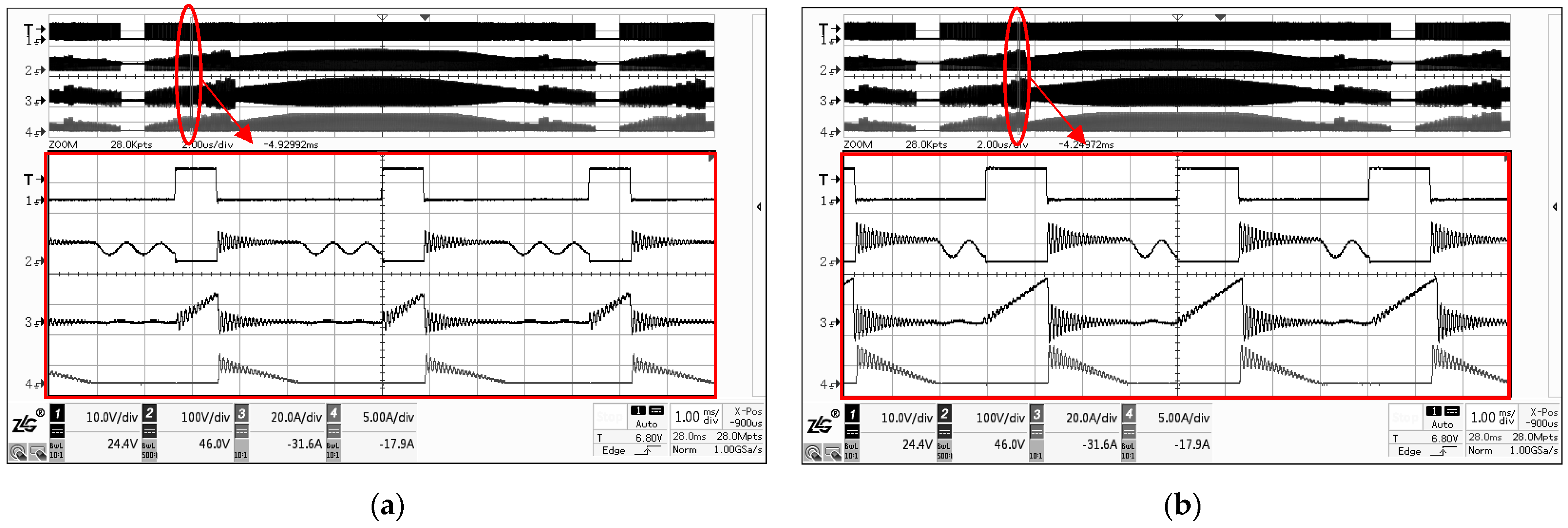
Figure 12 shows the waveforms PWM of the drive signals, MOSFET drain-source voltage UQ, transformer primary current Ip, and secondary current Is at a certain moment. It annotates the four time variables tcoss, toff, tr, and ton mentioned in Section 2.2. At this time, the transformer primary current oscillates and generates a turn-on signal for switch Q at the third valley bottom, achieving valley turn-on. The switching period of switch Q is 10.78 μs.
Figure 13 provides waveforms of the MOSFET Q voltage and transformer current under four different phase conditions. The multi-valley turn-on control strategy achieves valley turn-on in all cases. With increasing phase angle, Figure 13a–d represent the switch tube turn-on signals generated at the fifth, fourth, second, and first valleys of the oscillation, with switch periods of 14.72 μs, 13.01 μs, 8.95 μs, and 6.67 μs, respectively. The peak current changes with the variation in the phase angle. The multi-valley turn-on control strategy proposed in this paper can accurately calculate the reference current curve, thereby controlling the turn-on and turn-off signals of the switch in real time to achieve valley turn-on, reduce the energy impact during turn-on, decrease switch losses, and improve efficiency.
Figure 14 compares the efficiency between the multi-valley turn-on control strategy and the fixed-frequency control method from [28]. The proposed multi-valley turn-on control strategy effectively improves the operational efficiency.
Figure 15a shows the voltage and current waveforms of the fixed-frequency control strategy. Figure 15b shows the voltage and current waveforms of the proposed multi-valley turn-on control strategy. Because the primary current Ip of the transformer is much smaller than the grid voltage, for convenience of comparison, Ip is amplified three times.
When the grid phase is low, the envelope of the primary current using the control strategy proposed in this research is smoother, resulting in a smaller energy impact, and it effectively reduces the harmonic content. It can be seen that by using an accurate peak current reference curve, the system ensures precise turn-off signals, thus reducing the THD of the grid-connected current.
3.2. Experimental Validation
The microinverter prototype has its input connected to a single rooftop PV module and its output connected to a power grid simulator. Experiments were conducted in the central region of China (latitude 32° N, longitude 117° E) for a period of one year. The area experiences an annual temperature range of −6 °C to 42 °C, with an annual solar radiation of 1390–1630 kWh/m2. After one year of experimentation, it was demonstrated that this microinverter system proposed in this paper is capable of operating stably and continuously under various environmental conditions found in this region. In this section, the experimental results of the newly proposed control strategy are compared to those of the fixed-frequency turn-on control strategy.
Figure 16 presents the waveforms of the MOSFET Q in the DCM based on a fixed-frequency control strategy with different grid phase angles, where CH1 is the driving signal PWM of Q, CH2 is the drain-source voltage UQ of Q, and CH4 is the grid-connected current Igp. The fixed-frequency strategy cannot achieve valley turn-on for the MOSFET, resulting in the MOSFET bearing relatively large voltage stress at the moment of turn-on, causing component loss and a decrease in system efficiency.
Figure 17 provides detailed waveforms of key signals in the DCM based on the multi-valley turn-on control strategy. CH1 is the driving signal PWM of MOSFET Q, CH2 is the drain-source voltage UQ of MOSFET Q, CH3 is the primary current Ip of the transformer, and CH4 is the secondary current Is of the transformer. The experimental results are consistent with the theoretical analysis and simulated waveforms. Under different grid phases, the microinverter achieves multi-valley turn-on, effectively reducing the turn-on losses and heat losses of the MOSFET as much as possible, thereby improving the efficiency and verifying the feasibility of the control strategy. This control structure is also referred to as a quasi-resonant.
Another research by [27] proposed an optimising method based on a variable turn-off time in the DCM. However, this method requires additional comparator hardware to limit the peak inductance current, which increases the cost and volume of the inverter.
In order to compare the performance of the proposed multi-valley turn-on control strategy with the fixed-frequency control strategy, a comparison based on THD values is obtained as presented in Table 3. The proposed control strategy shows good values in terms of THD and can effectively reduce the harmonic content. The peak current control effect is good, and the grid-connected current waveform has a high sinusoidal degree.
From the perspective of system output, through a power analyser, it was found that the reactive power transmitted to the grid is basically 0; the effective value of the transmitted active power accounts for 95.2% of the maximum power under the corresponding conditions of the actual PV module, and the minimum efficiency observed within the tested range is 90.12% at an output power of 20 W.
Table 4 provides the performance metrics for all the control strategies mentioned in this paper under the full load condition. Through the comparative analysis, the superiority of the novel multi-valley turn-on control strategy proposed in this research in terms of improving efficiency and reducing harmonic content can be verified.
4. Conclusions
This paper proposes a quasi-resonant structure and control strategy for a photovoltaic flyback grid-connected microinverter. To reduce the energy impact, effectively decrease device losses and harmonic content, and enhance the stability of the microinverter and the quality of the grid-connected waveform, two key issues have been addressed:
- When the grid phase angle is small, the power is also low, and the switch tube has a very high frequency, which strongly affects the performance of the device, leading to increased device stress and switch losses. This paper introduces a topology structure that incorporates a compensation capacitor to increase the resonance period, addressing the issues of high switching frequency and increased losses.
- The reference current curve for conventional peak current control considers only ideal device conditions, which will affect the waveform for circuits with parasitic parameters. This paper proposes an optimised method for calculating the peak current reference curve, which can accurately calculate the reference waveform under actual engineering conditions, ensuring the accuracy of the turn-off signal. At the same time, a multi-valley turn-on method is proposed to reduce device losses and harmonic content of the grid-connected current.
Author Contributions
The contributions made by the authors are as follows: overall design framework and methodology: Z.C. and Y.H.; simulation: Z.C.; result analysis and interpretation: Z.C., A.b.J. and Y.H.; draft and manuscript preparation: Z.C., A.b.J. and A.Y.; overall supervision and resources: A.b.J. and A.Y. All authors have read and agreed to the published version of the manuscript.
Funding
This study is supported by Natural Science Research Project of Anhui Educational Committee of China (grant number 2023AH052662).
Data Availability Statement
The data are not publicly available due to privacy restrictions.
Conflicts of Interest
The authors declare no conflicts of interest.
References
- Sutikno, T.; Arsadiando, W.; Wangsupphaphol, A.; Yudhana, A.; Facta, M. A Review of Recent Advances on Hybrid Energy Storage System for Solar Photovoltaics Power Generation. IEEE Access 2022, 10, 42346–42364. [Google Scholar] [CrossRef]
- Kjaer, S.B.; Pedersen, J.K.; Blaabjerg, F. A review of single-phase grid-connected inverters for photovoltaic modules. IEEE Trans. Ind. Appl. 2005, 41, 1292–1306. [Google Scholar] [CrossRef]
- Li, Q.; Wolfs, P. A Review of the Single Phase Photovoltaic Module Integrated Converter Topologies with Three Different DC Link Configurations. IEEE Trans. Power Electron. 2008, 23, 1320–1333. [Google Scholar]
- Chiu, H.; Lo, Y.; Yang, C.; Cheng, S.; Huang, C.-M.; Chuang, C.; Kuo, M.; Huang, Y.; Jean, Y.; Huang, Y. A module-integrated isolated solar microinverter. IEEE Trans. Ind. Electron. 2013, 60, 781–788. [Google Scholar] [CrossRef]
- Shafiullah, M.; Ahmed, S.D.; Al-Sulaiman, F.A. Grid Integration Challenges and Solution Strategies for Solar PV Systems: A Review. IEEE Access 2022, 10, 52233–52257. [Google Scholar] [CrossRef]
- Tang, Z.; Yang, Y.; Blaabjerg, F. Power electronics: The enabling technology for renewable energy integration. CSEE J. Power Energy Syst. 2022, 8, 39–52. [Google Scholar]
- Tacca, H.E. Single-switch two-output flyback-forward converter operation. IEEE Trans. Power Electron. 1998, 13, 903–911. [Google Scholar]
- Bidram, A.; Davoudi, A.; Balog, R.S. Control and Circuit Techniques to Mitigate Partial Shading Effects in Photovoltaic Arrays. IEEE J. Photovolt. 2012, 2, 532–546. [Google Scholar]
- Meneses, D.; Blaabjerg, F.; García, Ó.; Cobos, J.A. Review and Comparison of Step-Up Transformerless Topologies for Photovoltaic AC-Module Application. IEEE Trans. Power Electron. 2013, 28, 2649–2663. [Google Scholar] [CrossRef]
- Kouro, S.; Leon, J.I.; Vinnikov, D.; Franquelo, L.G. Grid-Connected Photovoltaic Systems: An Overview of Recent Research and Emerging PV Converter Technology. IEEE Ind. Electron. Mag. 2015, 9, 47–61. [Google Scholar] [CrossRef]
- Díaz, M.; Muñoz, J.; Rivera, M.; Rohten, J. A Comprehensive Control Strategy for a Push–Pull Microinverter Connected to the Grid. Energies 2023, 16, 3196. [Google Scholar] [CrossRef]
- Front Matter. In Control of Power Electronic Converters and Systems; Blaabjerg, F. (Ed.) Academic Press: Cambridge, MA, USA, 2018; pp. i–ii. [Google Scholar] [CrossRef]
- Myrzik, J.M.A.; Calais, M. String and module integrated inverters for single-phase grid connected photovoltaic systems—A review. In Proceedings of the 2003 IEEE Bologna Power Tech Conference Proceedings, Bologna, Italy, 23–26 June 2003; Volume 2, p. 8. [Google Scholar]
- Scholten, D.M.; Ertugrul, N.; Soong, W.L. Micro-inverters in small scale PV systems: A review and future directions. In Proceedings of the 2013 Australasian Universities Power Engineering Conference (AUPEC), Hobart, Australia, 29 September–3 October 2013; pp. 1–6. [Google Scholar]
- Gong, X.; Josifović, I.; Ferreira, J.A. Modeling and Reduction of Conducted EMI of Inverters with SiC JFETs on Insulated Metal Substrate. IEEE Trans. Power Electron. 2013, 28, 3138–3146. [Google Scholar] [CrossRef]
- Cichowski, A.; Nieznanski, J. Self-tuning dead-time compensation method for voltage-source inverters. IEEE Power Electron. Lett. 2005, 3, 72–75. [Google Scholar] [CrossRef]
- Cheng, H.-C.; Shen, Y.-H.; Chen, W.-H. Parasitic extraction and power loss estimation of power devices. J. Mech. 2021, 37, 134–148. [Google Scholar] [CrossRef]
- Yaqoob, S.J.; Raham, J.K.; Sadiq, H.A. Analysis and Simulation of Current-source Flyback Inverter with Efficient BCM Control Strategy. WSEAS Trans. Electron. 2021, 12, 132–140. [Google Scholar] [CrossRef]
- Trubitsyn, A.; Pierquet, B.J.; Hayman, A.K.; Gamache, G.E.; Sullivan, C.R.; Perreault, D.J. High-efficiency inverter for photovoltaic applications. In Proceedings of the 2010 IEEE Energy Conversion Congress and Exposition, Atlanta, GA, USA, 2–16 September 2010; pp. 2803–2810. [Google Scholar]
- Sharma, R.; Ball, J.A.R. Unipolar switched inverter low-frequency harmonics caused by switching delay. IET Power Electron. 2009, 2, 508–516. [Google Scholar] [CrossRef]
- Blahník, V.; Peroutka, Z.; Žák, J.; Talla, J. Elimination of dead-time effect causing current distortion of single-phase power converters. In Proceedings of the 2012 15th International Power Electronics and Motion Control Conference (EPE/PEMC), Novi Sad, Serbia, 4–6 September 2012; pp. DS1e.3-1–DS1e.3-6. [Google Scholar]
- Ma, X. Research on the Control Method of the Inverter Based on Discontinuous Inductor Current Mode. Master’s Thesis, Huazhong University of Science & Technology, Wuhan, China, 2020. [Google Scholar]
- Fantino, R.A.; Christian, S.F.; Balda, J.C. Synchronous-Variable-Frequency Control of Bidirectional DCM Interleaved DC–DC Converter for Wide-Range Enhanced Efficiency. IEEE Trans. Ind. Electron. 2022, 69, 5844–5853. [Google Scholar] [CrossRef]
- Zhang, Z.; Zhang, J.; Shao, S. A Variable Off-Time Control Method for a Single-Phase DCM Microinverter. IEEE Trans. Power Electron. 2018, 33, 7229–7239. [Google Scholar] [CrossRef]
- Christidis, G.; Nanakos, A.; Tatakis, E. Optimal Design of a Flyback Microinverter Operating under Discontinuous-Boundary Conduction Mode (DBCM). Energies 2021, 14, 7480. [Google Scholar] [CrossRef]
- Pan, M.; Su, X.; Wang, Z. High efficiency solar energy single-stage grid-connected micro-inverter based on flyback topology. J. Mech. Electr. Eng. 2013, 30, 4. [Google Scholar]
- Lang, T.; Du, S.; Yin, H.; Hu, H. Optimizing Method for Light-Load Efficiency of a H-Bridge Inverter Based on Variable Turn-Off Time Discontinuous Current Mode. Trans. China Electrotech. Soc. 2020, 35, 4761–4770. [Google Scholar]
- Hasnain, A.; D’Antonio, M.; Singhabahu, C.; Shen, Y.; Zakzewski, D.; Khaligh, A. Optimal Modulation and DM Filter Design for a High Switching Frequency Single-Stage Microinverter. In Proceedings of the 2023 IEEE Applied Power Electronics Conference and Exposition (APEC), Orlando, FL, USA, 19–23 March 2023; pp. 1483–1488. [Google Scholar]
Figure 1.
Flyback inverter topology.

Figure 2.
Approximate waveforms of each stage in DCM.
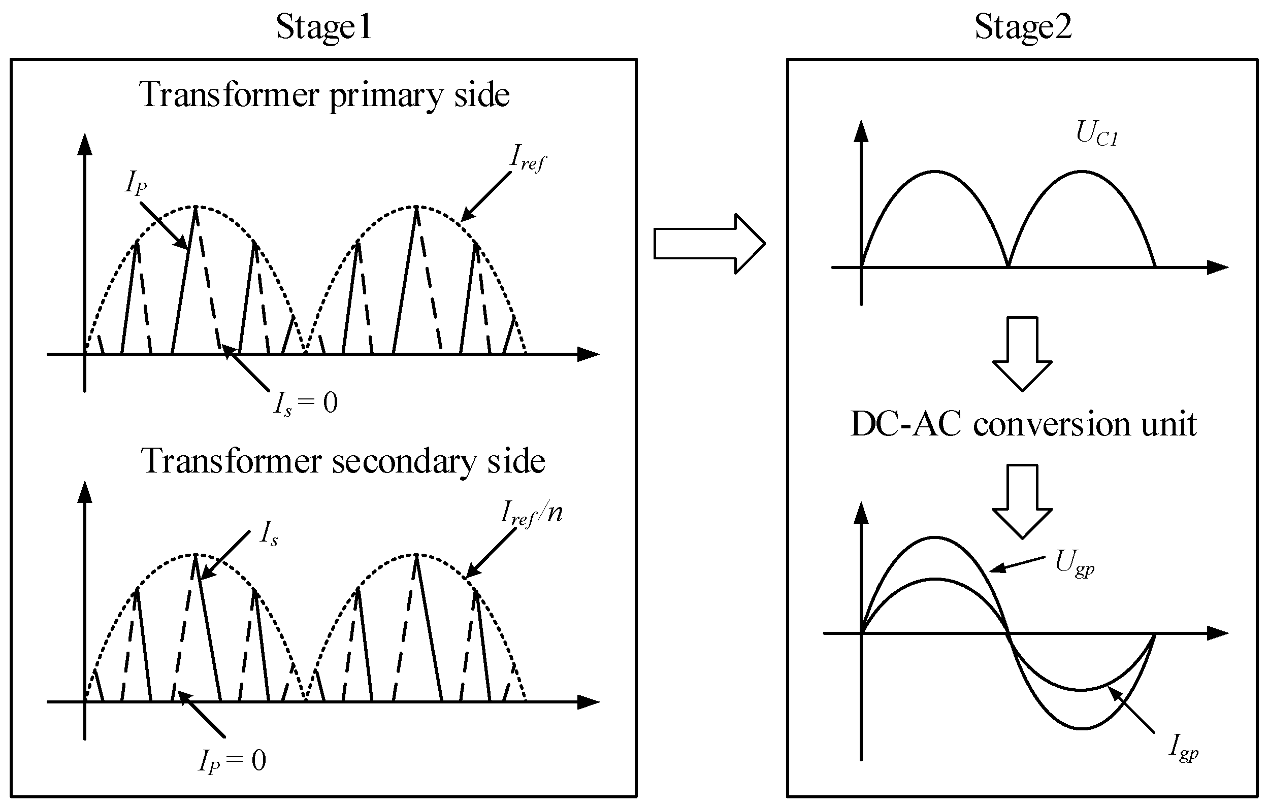
Figure 3.
Operating modes of the DCM flyback inverter: (a) Mode 1; (b) Mode 2; (c) Mode 3.

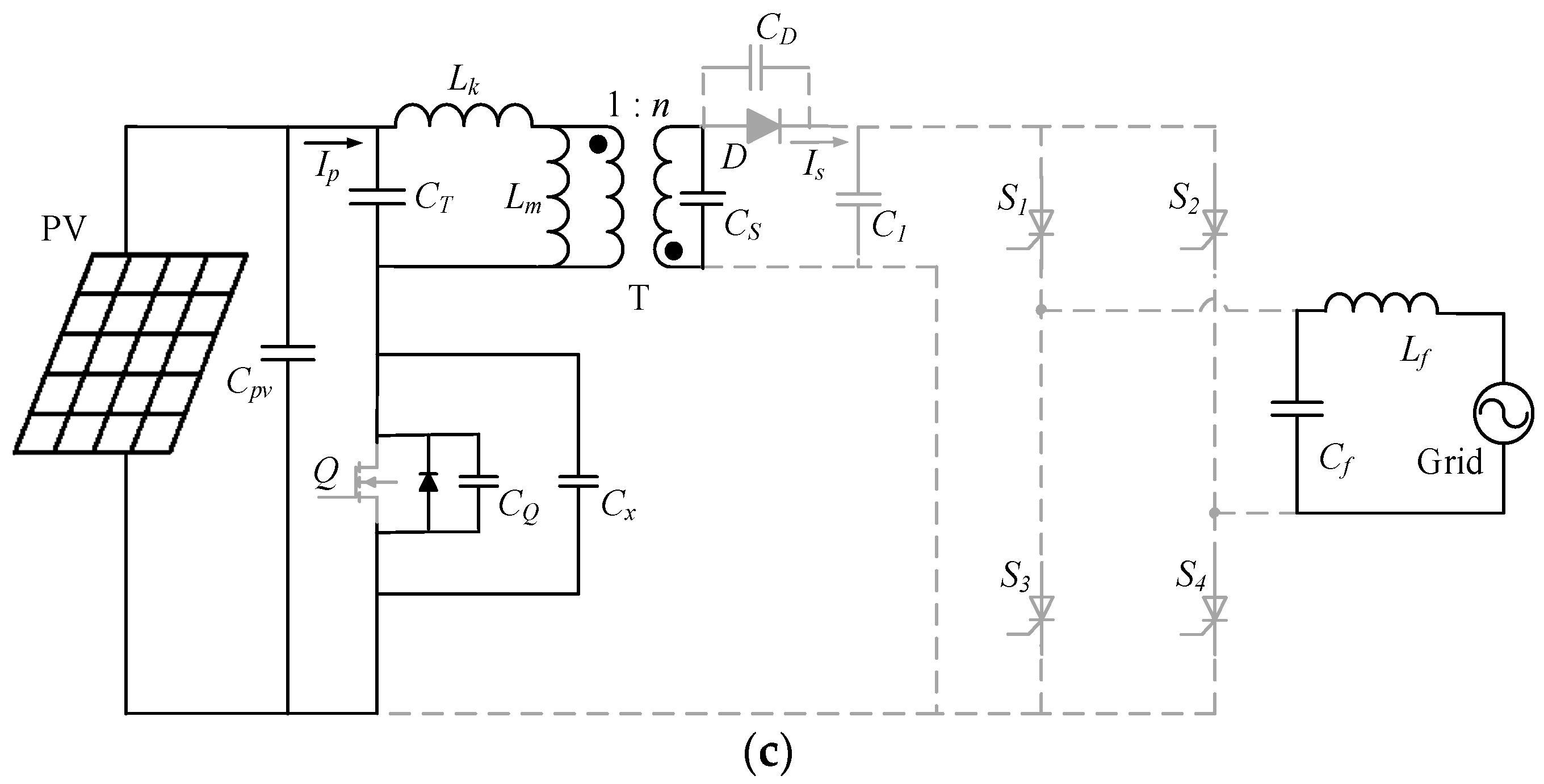
Figure 4.
Actual primary current curves under different initial values.
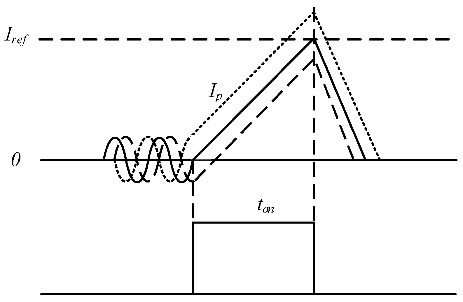
Figure 5.
Control strategy diagram of inverter.
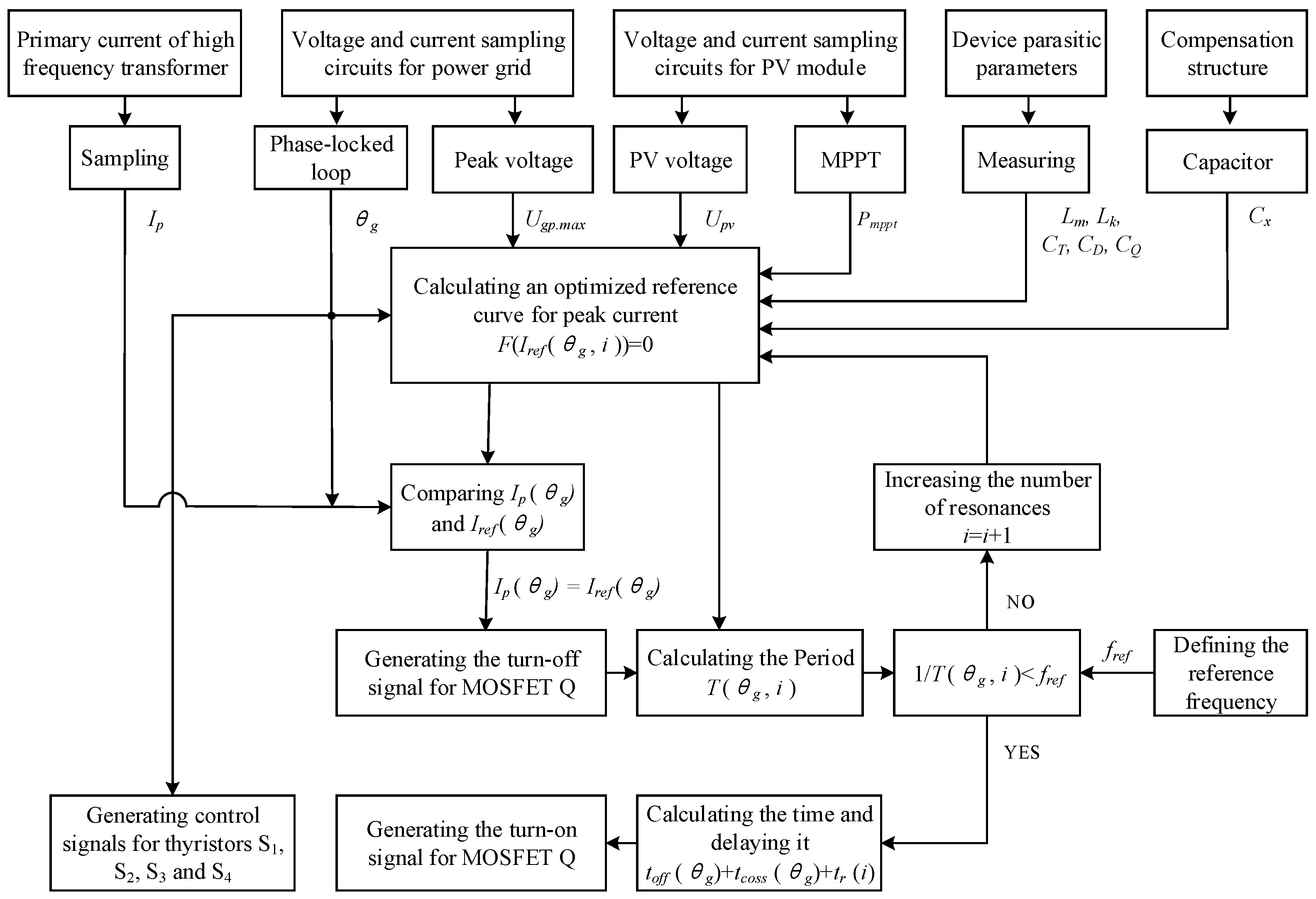
Figure 6.
Micro inverter prototype.
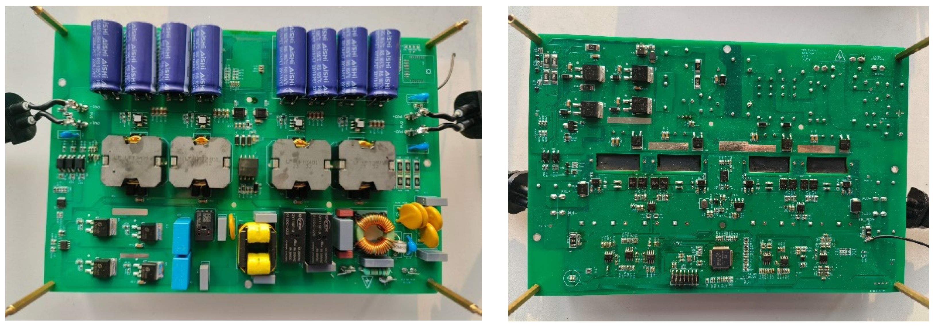
Figure 7.
Experimental platform.
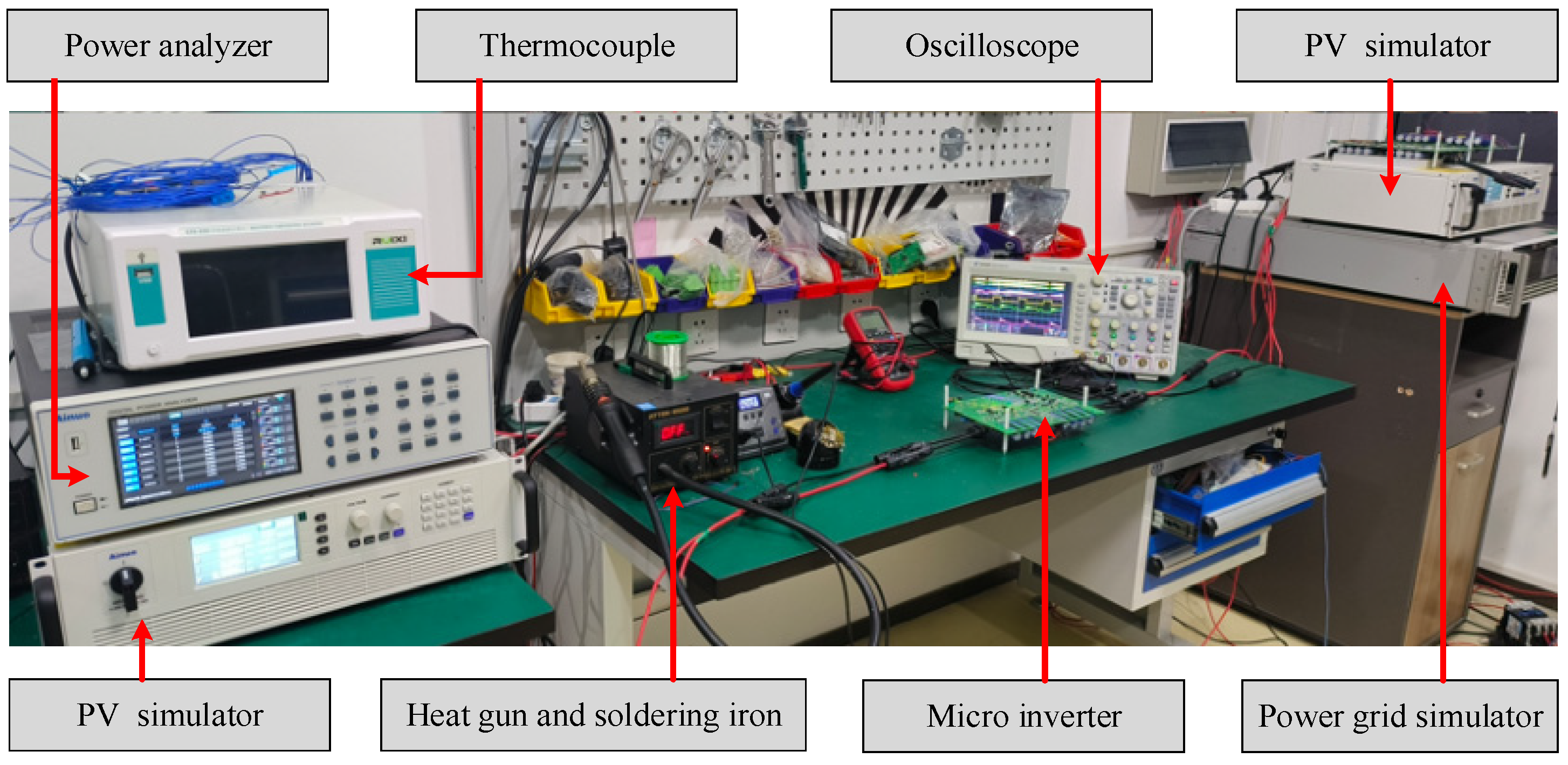
Figure 8.
Overall and detailed key waveforms.
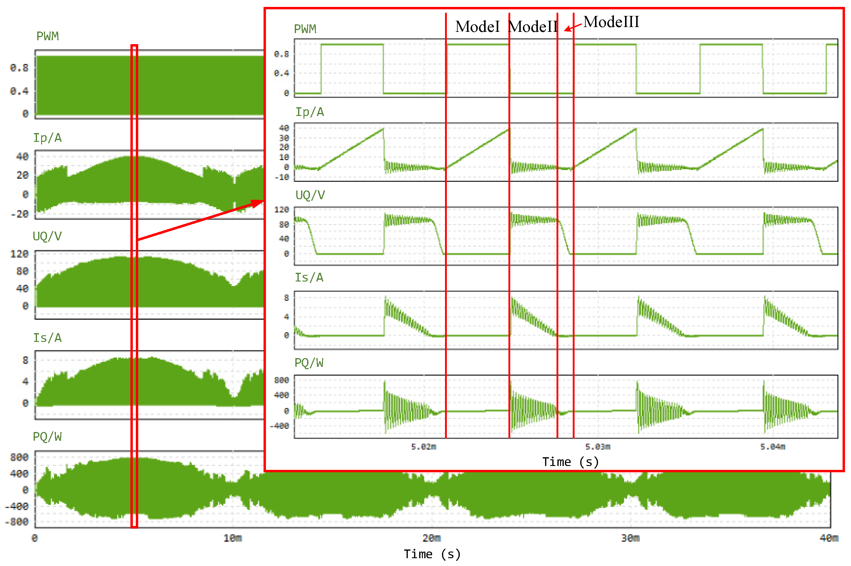
Figure 9.
Voltage across the switch before and after adding compensation capacitor: (a) Voltage across the switch Q without compensation capacitor; (b) Voltage across the switch Q with compensation capacitor.
Figure 9.
Voltage across the switch before and after adding compensation capacitor: (a) Voltage across the switch Q without compensation capacitor; (b) Voltage across the switch Q with compensation capacitor.

Figure 10.
Switch tube power loss with different Cx.
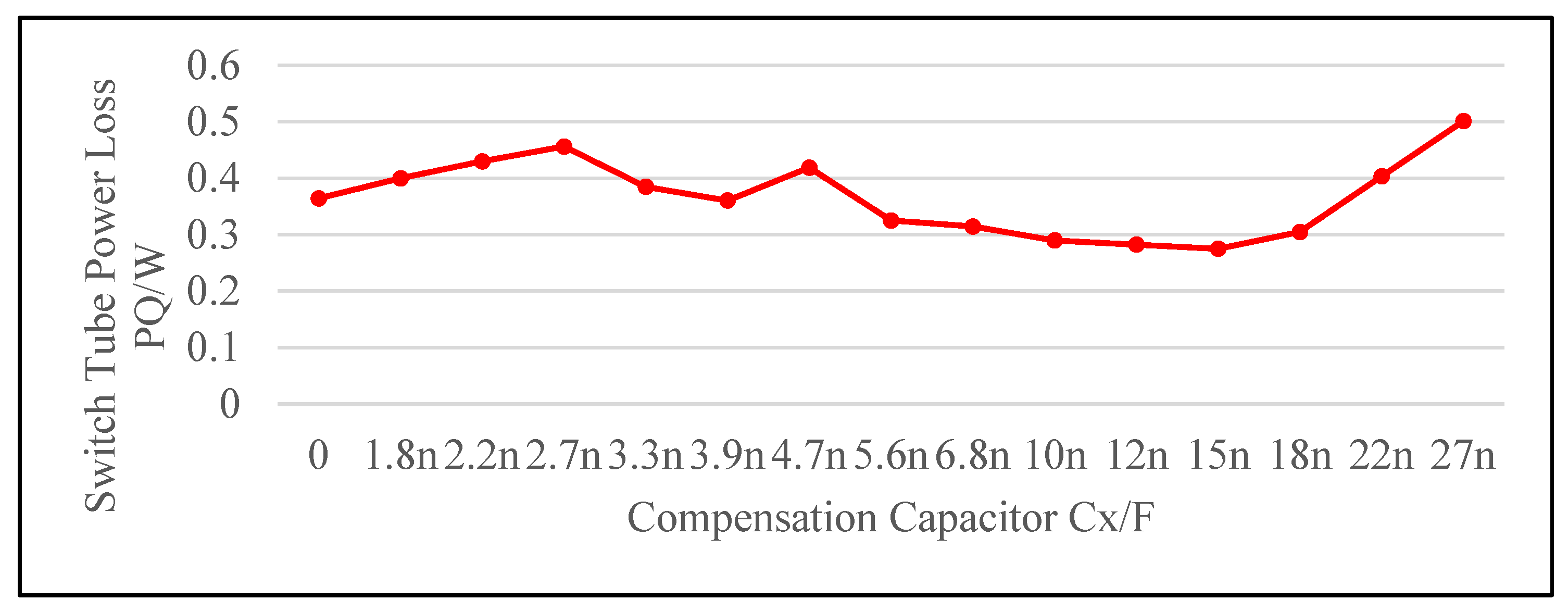
Figure 11.
Peak current reference curves for different numbers of resonances.

Figure 12.
Waveforms of switch tube voltage and transformer current.
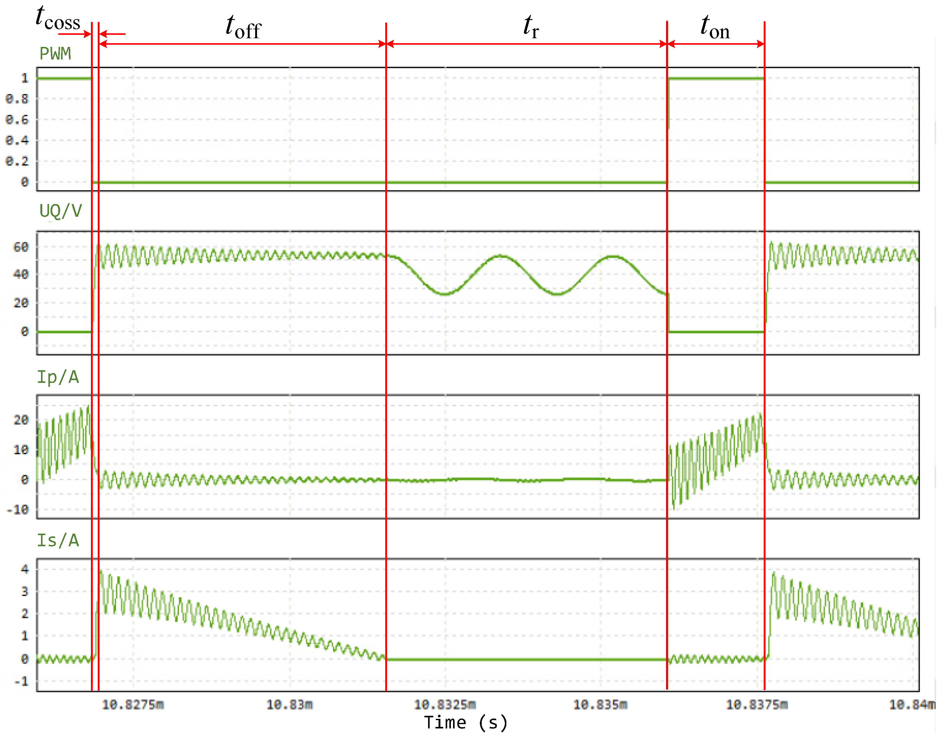
Figure 13.
Waveforms of switch Q voltage and transformer current at different phases: (a) Phase 1; (b) Phase 2; (c) Phase 3; (d) Phase 4.
Figure 13.
Waveforms of switch Q voltage and transformer current at different phases: (a) Phase 1; (b) Phase 2; (c) Phase 3; (d) Phase 4.
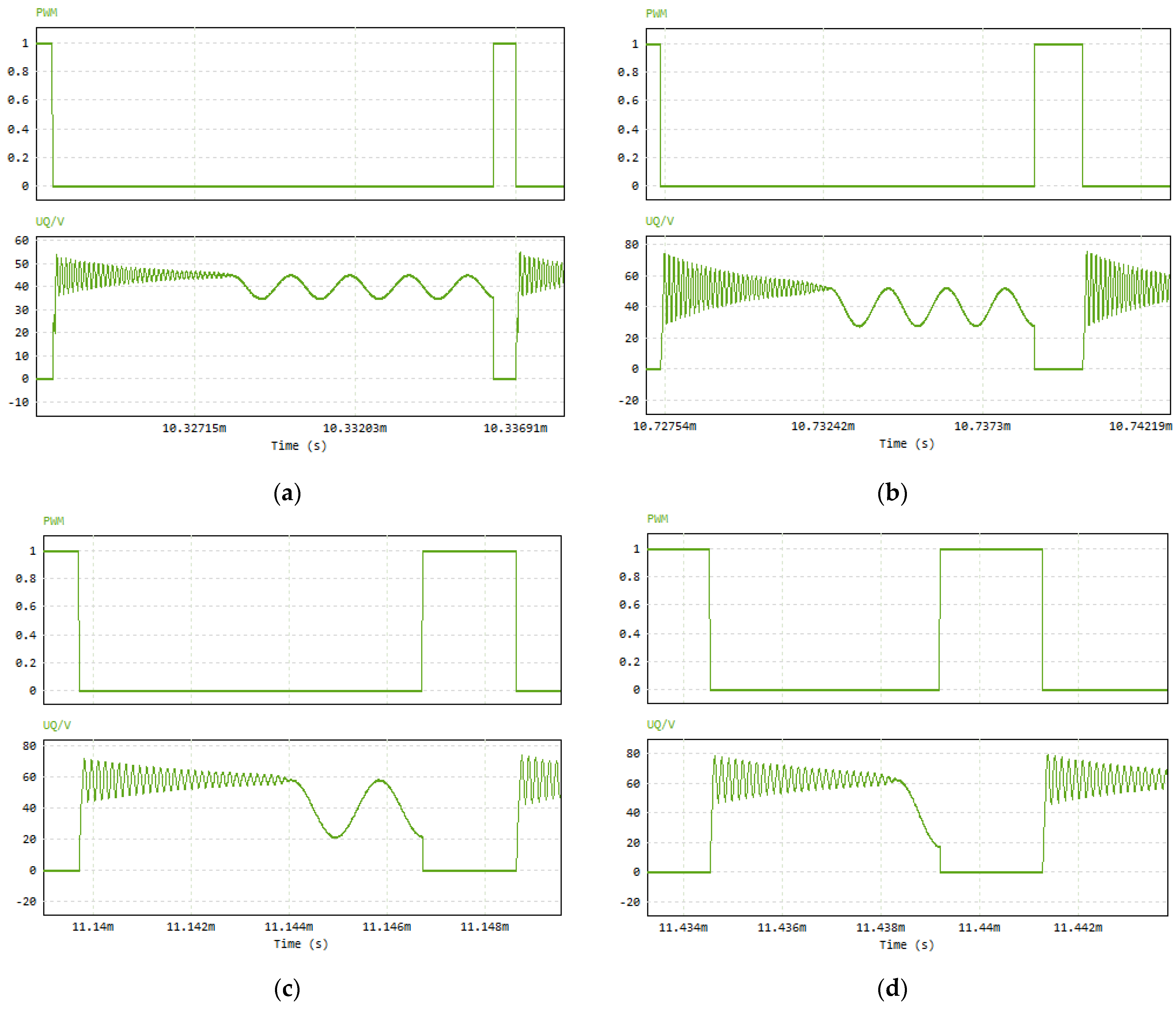
Figure 14.
Efficiency curves of the two strategies [28].
Figure 14.
Efficiency curves of the two strategies [28].
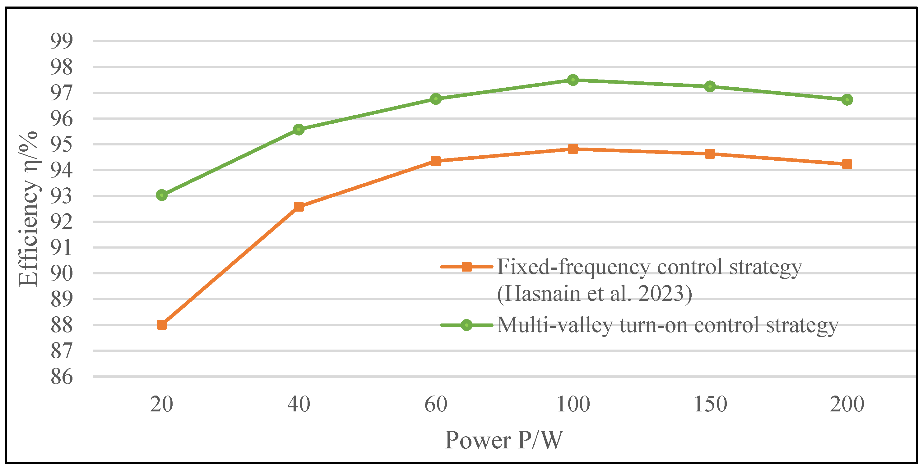
Figure 15.
Voltage and current waveforms of two strategies: (a) Fixed-frequency control strategy; (b) Multi-valley turn-on control strategy.
Figure 15.
Voltage and current waveforms of two strategies: (a) Fixed-frequency control strategy; (b) Multi-valley turn-on control strategy.
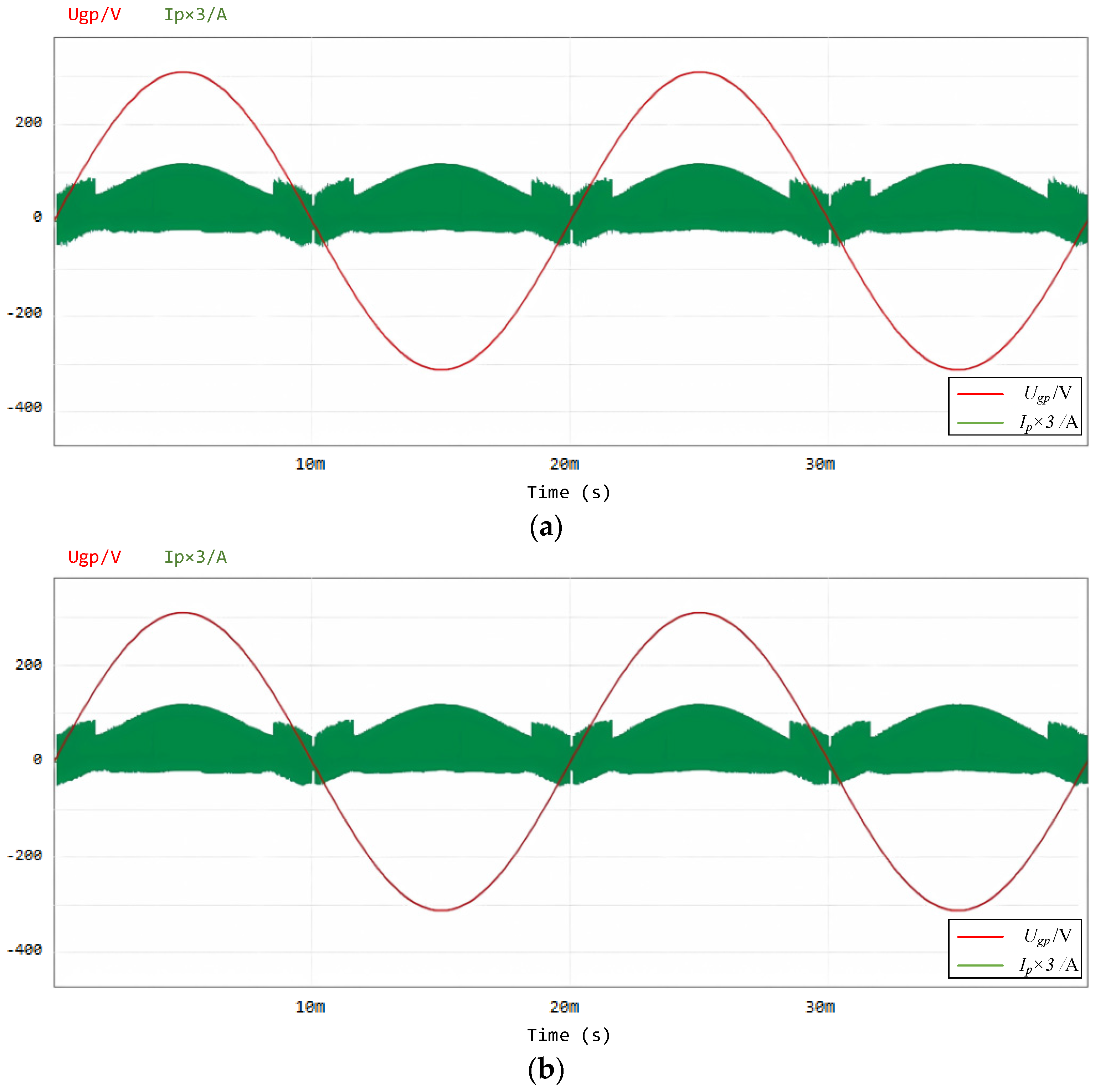
Figure 16.
MOSFET Q waveforms of the fixed-frequency control strategy: (a) Phase 1; (b) Phase 2.
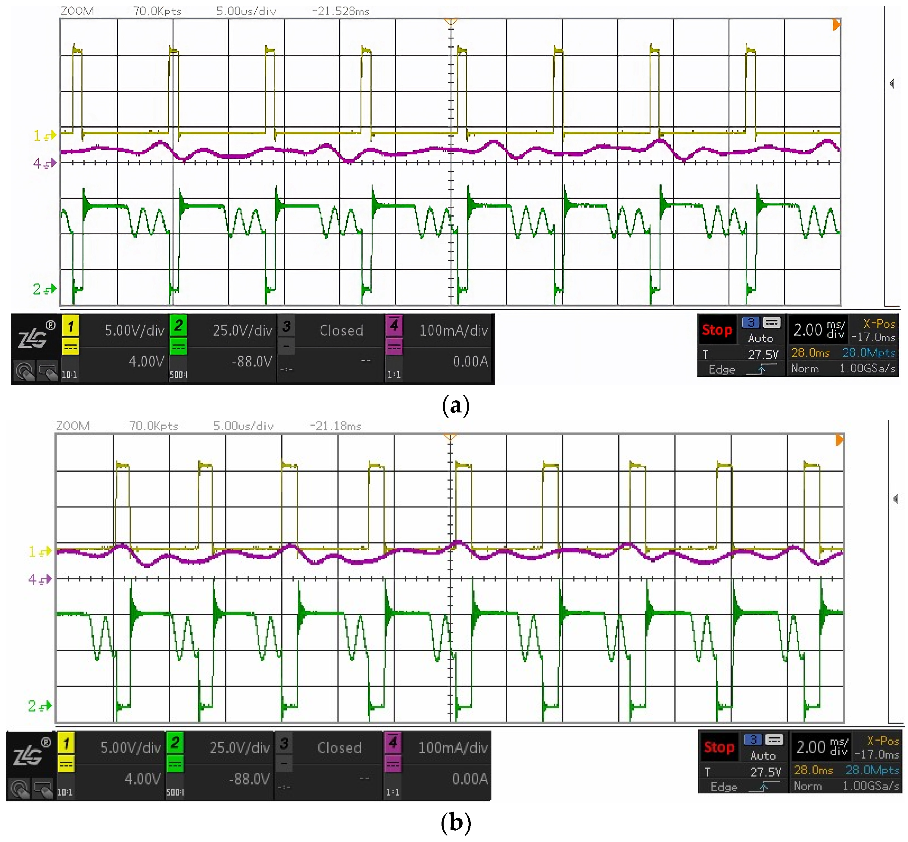
Figure 17.
Waveforms of various signals at different phases: (a) Phase 1; (b) Phase 2.

Table 1.
Key parameters of inverter.
| Parameter | Value | Unit |
|---|---|---|
| DC input voltage Upv | 25–55 | V |
| Effective value of AC output voltage Ugp | 220 | V |
| Output voltage frequency fgp | 50 | Hz |
| Rated output power P | 200 | W |
| Output filter capacitors C1 | 10n | F |
| Absorption capacitor CS | 220p | F |
| Grid-side capacitors Cf | 330n | F |
| Grid-side inductor Lf | 0.6m | H |
| Maximum switching frequency fmax | 300 | kHz |
| Ratio of transformer n | 2:12 | - |
Table 2.
Component parasitic parameters required for the control strategy.
| Parameter | Value | Unit |
|---|---|---|
| Excitation inductor Lm | 3.4u | H |
| Leakage inductor Lk | 34.2n | H |
| Distributed capacitor CT | 321.5p | F |
| Parasitic capacitor of transistor Q CQ | 321.5p | F |
| Parasitic capacitor of diode D CD | 22p | F |
Table 3.
Comparison of THD between other method and proposed method.
| Power (W) | 40 | 80 | 120 | 160 | 200 |
|---|---|---|---|---|---|
| Fixed-frequency control strategy | 6.32% | 5.04% | 4.43% | 4.00% | 3.87% |
| Multi-valley turn-on control strategy | 5.11% | 3.87% | 3.19% | 2.67% | 2.39% |
Table 4.
Comparison of the control strategies.
| Literature | Methods | Main findings | Drawbacks | Efficiency | THD |
|---|---|---|---|---|---|
| [18] | BCM control strategy suitable for medium and small power-level inverters | It achieved Zero Voltage Switching (ZVS) of the switch tube. | When operating at light load, the high switching frequency exacerbates turn-off losses. | / | 2.9% |
| [22] | DCM with fixed turn-off time for inductance current | The inverter efficiency under DCM is significantly higher than that under CCM. | When operating at light load, the switching frequency still increases. | 93.2% | 2.5% |
| [23] | Bidirectional DCM constant on-time variable-frequency control strategy | It enhanced the converter efficiency at low-power conditions. | This method is not applicable to the single-phase microinverters studied. | 96.7% | / |
| [24] | Variable turn-off time control method | It was effective in light load efficiency improvement. | It did not mention the issues of switch tube losses and harmonics. | 95.4% | / |
| [25] | Hybrid DBCM operation | It inherited the merits of both DCM and BCM. | It did not take into account the parasitic parameters. | 92.1% | / |
| [27] | Variable turn-off time method in DCM | It improved the quality of light-load current. | It required additional hardware to limit the peak inductance current. | 95.7% | 3.6% |
| This research | Multi--valley turn-on control strategy | Considering parasitic parameters, It minimised switch losses. | / | 95.2% | 2.4% |
Disclaimer/Publisher’s Note: The statements, opinions and data contained in all publications are solely those of the individual author(s) and contributor(s) and not of MDPI and/or the editor(s). MDPI and/or the editor(s) disclaim responsibility for any injury to people or property resulting from any ideas, methods, instructions or products referred to in the content. |
© 2024 by the authors. Licensee MDPI, Basel, Switzerland. This article is an open access article distributed under the terms and conditions of the Creative Commons Attribution (CC BY) license (https://creativecommons.org/licenses/by/4.0/).
Share and Cite
MDPI and ACS Style
Cao, Z.; Jamali, A.b.; Yassin, A.; Huang, Y. The Quasi-Resonant Structure and Control Strategy of a Photovoltaic Flyback Grid-Connected Microinverter. Electronics 2024, 13, 1903. https://doi.org/10.3390/electronics13101903
AMA Style
Cao Z, Jamali Ab, Yassin A, Huang Y. The Quasi-Resonant Structure and Control Strategy of a Photovoltaic Flyback Grid-Connected Microinverter. Electronics. 2024; 13(10):1903. https://doi.org/10.3390/electronics13101903
Chicago/Turabian StyleCao, Zipei, Annisa binti Jamali, Abdullah Yassin, and Ya Huang. 2024. "The Quasi-Resonant Structure and Control Strategy of a Photovoltaic Flyback Grid-Connected Microinverter" Electronics 13, no. 10: 1903. https://doi.org/10.3390/electronics13101903
Note that from the first issue of 2016, this journal uses article numbers instead of page numbers. See further details here.