Article

A Proposed Single-Input Multi-Output Battery-Connected DC–DC Buck–Boost Converter for Automotive Applications

1
Seger Ses ve Elektrikli Gereçler San. A.Ş., 16110 Bursa, Turkey
2
Power Electronics Center of Electrical and Electronics Engineering Research Laboratories, Bursa Technical University, Yıldırım, 16310 Bursa, Turkey
*
Author to whom correspondence should be addressed.
Electronics 2023, 12(20), 4381; https://doi.org/10.3390/electronics12204381
Submission received: 21 September 2023 / Revised: 12 October 2023 / Accepted: 17 October 2023 / Published: 23 October 2023

Abstract

:
In the realm of electric vehicles (EVs), achieving diverse direct current (DC) voltage levels is essential to meet varying electrical load demands. This requires meticulous control of the battery voltage, which must be adjusted in line with specific load characteristics. Therefore, the integration of a well-designed power converter circuit is crucial, as it plays a pivotal role in generating different DC voltage outputs. In this study, we also consider the incorporation of two additional doubler/divider circuits at the end of the proposed converter, further enhancing its capacity to produce distinct DC voltage levels, thus increasing its versatility. The standout feature of the proposed converter lies in its remarkable ability to amplify DC voltages significantly. For instance, when the input battery voltage is set at 48 VDC with a duty cycle (D) of 0.8, the resulting output demonstrates a remarkable augmentation, producing voltages 18, 36, and 72 times higher than the input voltage. Conversely, with a reduced D of 0.2 while maintaining the input voltage at 48 VDC, the converter yields diminished voltages of 0.1875, 0.375, and 0.75 times the initial voltage. This adaptability, based on the parameterization of D, underscores the converter’s ability to cater to a wide range of voltage requirements. To oversee the intricate operations of this versatile converter, a high-speed DSP-based controller system is employed. It utilizes the renowned PID approach, known for its proficiency in navigating complex, nonlinear systems. Experimental results validate the theoretical and simulation findings, reaffirming the converter’s practical utility in EV applications. The study introduces a simple control mechanism with a single power switch, high efficiency for high-power applications, wide voltage range, especially with VDC and VMC cells, and continuous current operation for the load in CCM mode. This study underscores the significance of advanced power conversion systems in shaping the future of electric transportation.

1. Introduction

Power electronics-based DC–DC converters hold a critical role in contemporary electrical systems, facilitating effective voltage regulation and power transmission across a diverse array of applications [1,2,3]. Among the multitude of applications, electric vehicles (EVs) stand as a prominent exemplar. EVs epitomize the vanguard of sustainable transportation solutions, with the electrification of automotive powertrains becoming increasingly pervasive. A fundamental facet of EV power management is the DC–DC buck–boost converter, which plays a pivotal role in maintaining stable DC voltage levels as necessitated by various vehicle subsystems [4,5]. This article introduces a single-input and multi-output (SIMO) DC–DC buck–boost converter topology tailored for EVs, with a focus on elucidating its operational characteristics, advantages, and constraints.
DC–DC buck–boost converters, aptly named for their ability to both lower voltage (buck operation) [6] and elevate voltage (boost operation) [7,8] from a solitary input voltage source, function via the regulation of duty cycle, orchestrating energy transfer between input and output stages. Precision in voltage regulation is realized through common control methods such as pulse-width modulation (PWM).
Numerous DC–DC buck–boost converter types have been proposed for EV applications. This classification encompasses non-isolated [9,10,11], isolated [12,13,14], and bidirectional converter categories [15,16,17]. Non-isolated buck–boost converters are lauded for their simplicity and efficiency, rendering them apt for low- to medium-power applications in electric vehicles. This article delves into an array of non-isolated buck–boost converter topologies, notably the inductor–capacitor–inductor (L-C-L) and inductor–capacitor–diode (L-C-D) configurations. Noted for their uncomplicated design, non-isolated buck–boost converters incorporate fewer components compared to their isolated counterparts, translating into cost-effectiveness and superior overall efficiency, thus rendering them an appealing choice for low- to medium-power applications in EVs [18,19].
The compact form factor of these converters lends itself to facile integration within confined spaces in electric vehicles, harmonizing with the constraints prevalent in modern EV design. Their exceptional adaptability allows them to uphold steady output voltage levels even amid fluctuations in the input voltage, a pivotal advantage in EVs where battery voltage undergoes considerable variation contingent on charging and discharging conditions. However, non-isolated buck–boost converters exhibit a notable limitation, as they lack galvanic isolation between input and output. In scenarios where isolation is paramount, whether for safety or noise mitigation in high-voltage EV systems or sensitive electronic circuits, this deficiency presents challenges. Additionally, non-isolated buck–boost converters may demonstrate amplified voltage ripple on their output compared to their isolated counterparts, necessitating supplementary filtering measures to meet voltage quality standards. Although highly efficient for low- to medium-power applications, the inherent design limitations make them less suitable for high-power EV systems, where isolated converters are often favored, offering the requisite isolation and scalability.
Isolated buck–boost converters garner preference in high-power EV applications, where galvanic isolation assumes a pivotal role in safety and performance [20,21,22]. These converters encompass diverse isolation techniques, such as transformer-based [23] and coupled-inductor topologies [24], each accompanied by their distinct advantages and trade-offs. Foremost among the benefits of isolated buck–boost converters is their competence in ensuring galvanic isolation, thus mitigating the risk of electrical shock and reducing the potential for ground faults [25,26,27]. The role of isolation extends to curtailing electromagnetic interference (EMI) and radiofrequency interference (RFI) by containing electrical noise within the converter, particularly invaluable in EVs housing sensitive electronic components and communication systems, necessitating a low-noise environment to ensure peak performance. Isolated buck–boost converters exhibit flexibility in maintaining stable output voltage levels despite the fluctuating battery voltages typical of EV charging and discharging cycles. However, it is important to note that isolated converters tend to be more intricate and expensive to design and manufacture than their non-isolated counterparts. The inclusion of isolation components, such as transformers, introduces energy losses, diminishing overall efficiency when compared to non-isolated converters. This efficiency trade-off may be acceptable in certain applications, but may not align with the stringent efficiency benchmarks of high-performance EV systems. The need for isolation components and associated circuitry results in a larger physical footprint for isolated buck–boost converters, which can pose challenges in EVs with constrained space for power electronics.
The third category of buck–boost converters encompasses bidirectional converter types [28,29,30]. Bidirectional converters assume a pivotal role in energy recuperation in EVs, enabling the transfer of energy between the vehicle’s battery and the electrical grid [31,32,33]. A key advantage of bidirectional buck–boost converters lies in their ability to efficiently recover and reuse energy. This feature is particularly valuable during regenerative braking events in EVs, where the converter captures and stores energy that would otherwise dissipate as heat. The recuperated energy can subsequently replenish the vehicle’s battery, bolstering overall efficiency and extending driving range. Bidirectional converters are exceptionally adaptable to variable input and output voltage requirements, offering versatility in EV power management, particularly vital in electric and hybrid vehicles where battery voltage exhibits significant variation due to charging, discharging, and load fluctuations. Bidirectional buck–boost converters play a pivotal role in vehicle-to-grid (V2G) applications, enabling EVs to serve as energy storage systems. This enables the bidirectional flow of energy between the EV’s battery and the grid, allowing for energy injection during peak demand periods and potentially serving as a revenue source for EV owners.
The bidirectional operation of these converters necessitates intricate control algorithms to accurately manage bidirectional power flow, often requiring advanced DSP or microcontroller-based control systems. While bidirectional buck–boost converters excel at energy recovery, they may not consistently achieve the same high efficiency as unidirectional converters due to the added complexity involved in managing bidirectional power flow. Energy losses during bidirectional operation can impact overall efficiency. The incorporation of bidirectional functionality and associated control circuitry can escalate the cost and physical size of these converters compared to their unidirectional counterparts, potentially posing challenges in space-constrained EV power electronics designs.
This study introduces a single-input and multi-output (SIMO) DC–DC buck–boost converter. Multi-output buck–boost converters are renowned for their versatility in generating multiple DC voltage outputs from a single input source. This versatility is particularly advantageous in EVs where diverse subsystems and components may necessitate varying voltage levels for optimal performance. These converters can accommodate the varied voltage requirements of propulsion systems, auxiliary loads, and energy storage systems within the vehicle. In the confined confines of an electric vehicle, where efficient space utilization and weight management take precedence, multi-output buck–boost converters assume a pivotal role. By consolidating multiple voltage conversion functions into a single device, these converters curtail the overall footprint and weight of power electronics, freeing up space for other essential components like batteries or passenger amenities. This consolidation contributes to cost savings and simplifies the bill of materials, reducing manufacturing complexity and potential points of failure, ultimately enhancing reliability. These converters are engineered to optimize energy efficiency by minimizing energy losses during the conversion process. In the context of electric vehicles, where energy conservation is paramount for extending driving range, multi-output buck–boost converters are instrumental in optimizing power utilization and consequently elevating overall efficiency. Furthermore, these converters facilitate compliance with voltage standards and safety requirements for EVs, ensuring precise regulation and maintenance of voltage levels within permissible limits to guarantee the safe and reliable operation of various vehicle systems.
DC–DC buck–boost converters employed in electric vehicles (EVs) implement various control methods, each possessing its own set of advantages and disadvantages. Prominent control methodologies encompass the fuzzy logic controller (FLC) [34,35,36,37,38], model predictive controller (MPC) [39,40], and proportional–integral–derivative (PID) controller [41,42,43].
FLC excels in handling complex and nonlinear systems, rendering it well suited for the dynamic and diversified voltage regulation requirements in EVs. It possesses the capacity to adjust the duty cycle and control parameters in real time, accommodating fluctuations in input voltage, load conditions, and temperature. This control approach incorporates linguistic variables and rules, effectively handling imprecise or uncertain information—a vital attribute in EVs where variable operating conditions and component variations can challenge conventional control methods. FLC presents a relatively straightforward implementation and tuning process compared to other control methods, diminishing development time and costs. Nevertheless, it is important to acknowledge that while fuzzy logic controllers offer advantages in handling imprecise and uncertain data, they may not be the optimal choice for all control applications, especially in complex and safety-critical systems like buck–boost converters in EVs. The choice of a control method should be contingent on a comprehensive evaluation of the specific requirements, constraints, and characteristics of the system in question. Possible disadvantages of FLC encompass rule base complexity, performance tuning, limited transparency, resource intensity, challenges in managing nonlinearity, and limited adaptability.
MPC can optimize control actions over a future prediction horizon, positioning it to deliver superior performance when addressing the variable and dynamic voltage requirements inherent in EVs. It is capable of simultaneously controlling multiple variables, affording more comprehensive power management in EVs. Nevertheless, MPC algorithms can be computationally intensive and complex to implement, potentially limiting their real-time applicability in certain EV systems. The predictive nature of MPC may introduce a delay in control actions, potentially posing challenges in applications necessitating rapid responses.
PID control is celebrated for its stability and robustness in regulating systems, a quality that proves advantageous in maintaining precise voltage levels within EVs. These controllers offer a straightforward tuning process, enabling the adjustment of proportional, integral, and derivative gains to achieve the desired response. The deployment of a PID controller in a buck–boost converter for EVs delivers stability, rapid response, eradication of steady-state error, noise rejection, adaptability, simplicity of implementation, and a proven track record of success. These advantages collectively contribute to the efficient and reliable operation of power electronics in EVs, ensuring consistent power delivery and safeguarding sensitive electronic components.
The proposed converter in this study adopts a non-isolated switched-inductor-based SIMO DC–DC buck–boost converter. The proposed converter incorporates a microcontroller, with a PID approach being implemented. The standout feature of this converter lies in its remarkable capacity to significantly amplify or attenuate DC voltages. For example, when the input battery voltage is set at 48 VDC with a duty cycle (D) of 0.8, the resulting output undergoes a remarkable enhancement, yielding voltages that are 18, 36, and 72 times higher than the input voltage. Conversely, by reducing D to 0.2 while maintaining the input voltage at 48 VDC, the converter generates lower voltages at 0.1875, 0.375, and 0.75 times the original voltage. This adaptability, contingent on the value of D, underscores the converter’s capability to meet a broad spectrum of voltage requirements.
The key advantages and innovations in this study can be condensed into the following: the adoption of a straightforward control mechanism, underpinned by the fact that the proposed topology features just one power switch; the high efficiency of the topology, making it well suited for high-power applications; the capacity to generate a broad voltage range, particularly when employing VDC and VMC cells; and the operation of the inductors in a continuous conduction mode (CCM), ensuring a consistent current state for the load.
Section 2 outlines the proposed topology, gain calculations, and the incorporation of VDC and VMC cells using the proposed control mechanism, while Section 3 discusses simulation and experimental results for various working modes and duty ratios, with Section 4 concluding the study and presenting numerical test results.

2. Materials and Methods

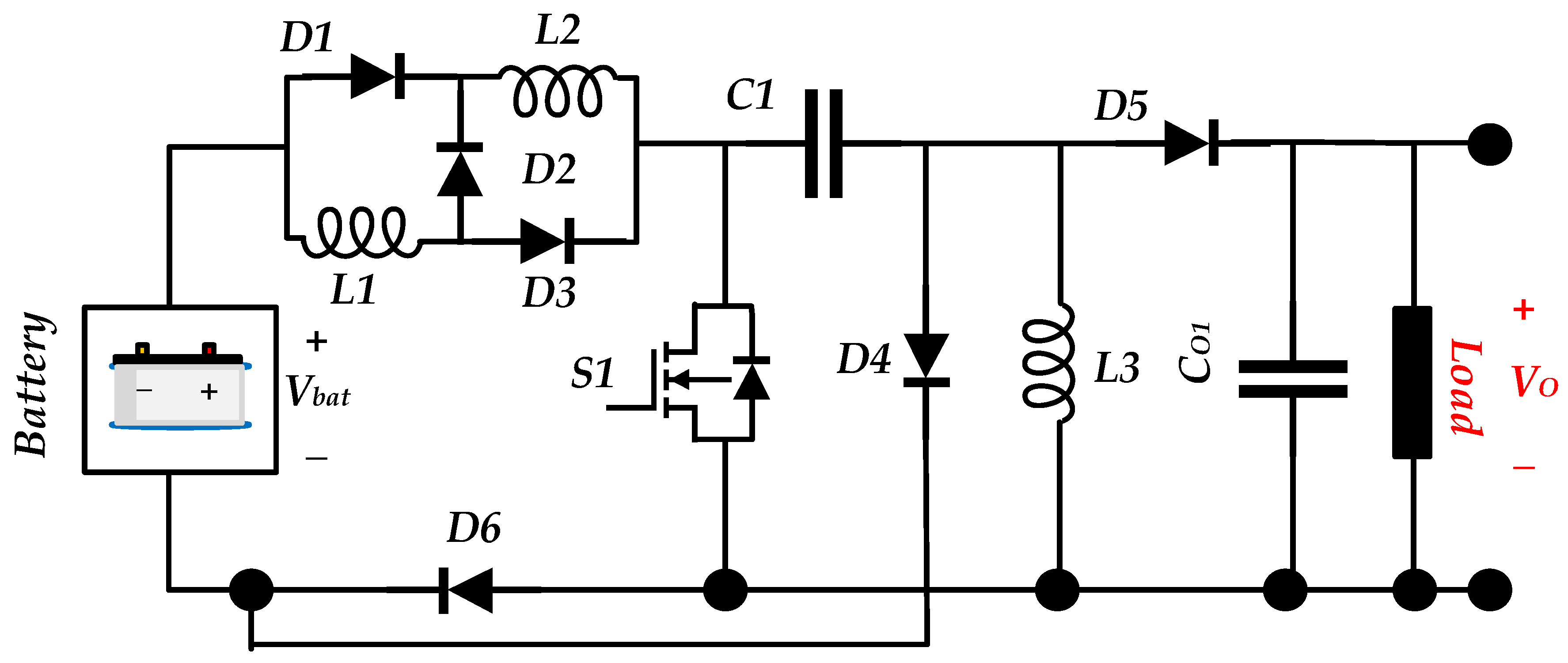
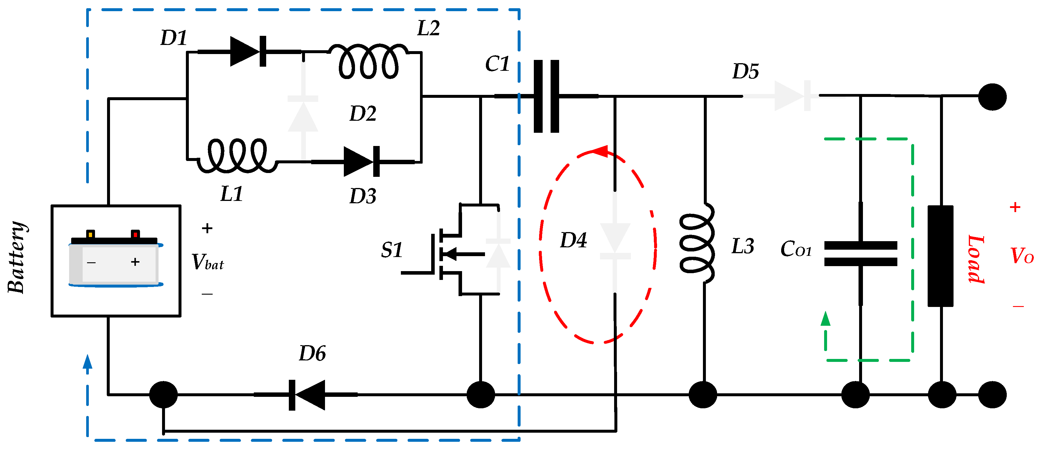
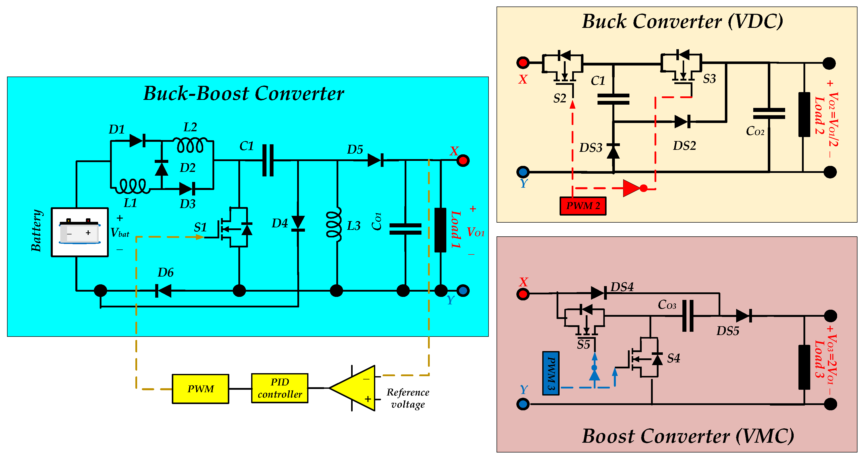
2.1. The Proposed Converter

In Figure 1, the proposed buck–boost converter is depicted, which incorporates a switched-inductor cell designed to enhance its suitability for high-power applications. This cell comprises diodes D1, D2, and D3, as well as inductors L1 and L2. When switch S1 is activated, both inductors, L1 and L2, are charged simultaneously, resulting in a reduction in the input current ripple sourced from the battery on the input side. Consequently, this minimizes the current ripple in the battery pack, thereby extending the battery’s lifespan. The remaining components of the converter closely resemble those of a single-ended primary inductance converter (SEPIC) [44,45]. Notably, this converter employs only a single power switch, simplifying the control process significantly.
In the analysis of a power converter circuit, we delve into two distinct modes: the switch-on state and the switch-off state. Each state brings about a change in the converter’s configuration, resulting in the derivation of a new set of equations. This section comprehensively examines both of these states. Assuming the switching time period of the power switch is denoted “T”, we can define the time intervals during which the switch is activated as “DT” and when it is deactivated as “(1-D)T”. Figure 2 visually illustrates these switching time intervals.
In the initial state, as depicted in Figure 3, when the switch is activated, both inductors L1 and L2 are connected in parallel with the input battery source, initiating the charging process. At this point, the voltage across these inductors equals the voltage of the battery itself.
L 1 · d i L 1 d t = L 2 · d i L 2 d t = V i n
The voltage on capacitor C1 is discharged on the inductor L3 through the switch:
L 3 · d i L 3 d t = V C 1
C 1 · d v C 1 d t = i L 3
During this operational mode, diodes D4 and D5 are in the off state. Consequently, during this time interval, the voltage across the output capacitor CO1 will discharge into the load.
C O 1 · d v C O 1 d t = v O 1 R O
The configuration of the converter during the time intervals when the switch is deactivated can be observed in Figure 4. In this operational mode, diodes D1 and D2 are disconnected, and inductors L1 and L2 are in series with the input battery source. During this mode, capacitor C1 is charging using the battery voltage. It is important to note that this capacitor was in a discharging mode during the first state.
The voltage across inductors L1 and L2 in the described operational modes can be obtained by applying Kirchhoff’s voltage law (KVL) to the relevant circuit configuration. The voltage on inductors L1 and L2 is obtained by:
L 1 · d i L 1 d t + L 2 · d i L 2 d t = ( V i n V C 1 ) ( 1 D )
Inductor L3 begins to discharge into the load by charging the output capacitor CO1.
L 3 · d i L 3 d t = V O 1 ( 1 D )
C 1 · d v C 1 d t = i L 3 ( 1     D )
C 0 · d v O 1 d t = i L 3 V O 1 R O 1 ( 1 D )
In line with the inductor’s second balance theorem, the average voltage across an inductor is determined to be zero. Consequently, this principle can be applied to inductors L1 and L2, leading to the following expression:
0 D T V i n d t + 1 2 D T T ( V i n V C 1 ) d t = 0
V i n D T + 1 2 ( V i n V C 1 ) ( 1 D ) = 0
The voltage across the capacitor C1 can be determined as follows:
V C 1 = V i n 1 + D 1 D
A similar theorem can be applied to inductor L3, resulting in an equation relating the input and output voltage as follows:
0 D T V C 1 d t + D T T V C O 1 d t = 0
G = V C O 1 V i n = D ( 1 + D ) ( 1 D ) 2
Equation (13) represents the gain of the proposed converter. This equation highlights the converter’s ability to achieve very low or high output voltages for different loads connected to the converter’s output side. When comparing the proposed converter to a conventional or SEPIC boost converter, it becomes evident that the achieved gain is quite substantial. Specifically, for a duty cycle (D) of 0.33 in the proposed converter, the output voltage matches the input battery source, whereas in a SEPIC converter, this same voltage is obtained at a duty cycle of 0.5. To visualize this comparison, Figure 5a,b provide graphical representations of the proposed converter and the conventional SEPIC converter for D values below and above 0.5, respectively.
Another crucial feature of the suggested converter is that it generates a positive output voltage without requiring a voltage-inverting circuit. This addresses a common issue found in conventional buck–boost converters.

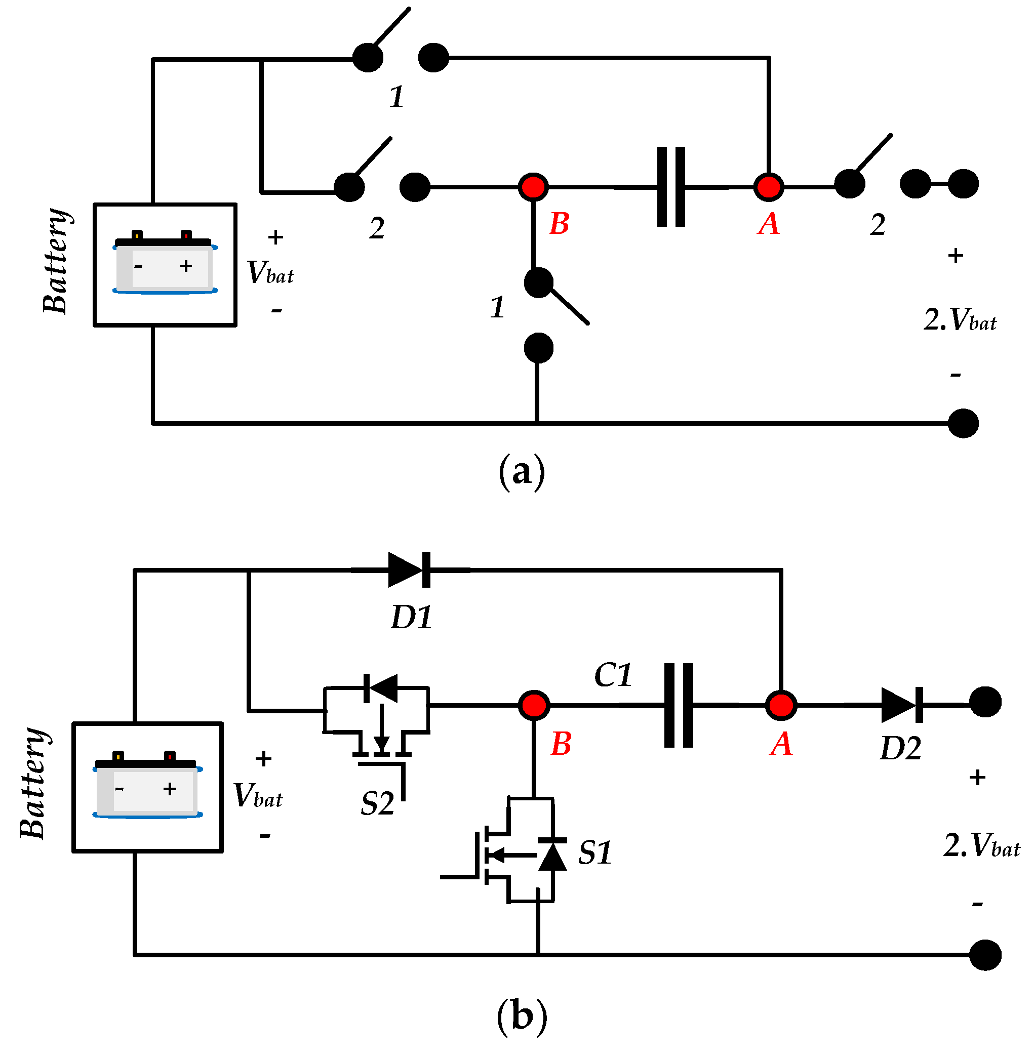
2.2. Voltage Multiplier Circuit (VMC)

A common application of the switched capacitor converter is in boost converters. To double the voltage across the source, a capacitor is initially connected between the source and the load. This capacitor, after storing the battery voltage, is then linked in series with the source, resulting in an output voltage of 2 Vbat. The schematic for achieving this is depicted in Figure 6a. Here, switch pair 1 operates in a phase opposite to switch pair 2: switch pair 1 closes and subsequently opens to charge the capacitor, while switch pair 2 closes to yield an output of 2 Vbat. Switches can be implemented using transistors alone or transistors in conjunction with diodes, as illustrated in Figure 6b. Transistor S1 is initially open, allowing C1 to charge to Vbat through D1. Following this, S1 is closed, and S2 is open.
The operational principles of the suggested VMC (voltage multiplier cell) are depicted in Figure 7a,b. Initially, a switching sequence is initiated, activating switch S1 while switch S2 remains without a positive driving pulse. During this time interval, capacitor C1 is charged from the power source, as illustrated in Figure 7a.
Once capacitor C1 is charged to Vbat, switch S1 is deactivated and switch S2 is activated. Consequently, diode D1 turns off, and D2 comes into operation. This state is visualized in Figure 7b, resulting in an output voltage twice the input voltage at the output point.

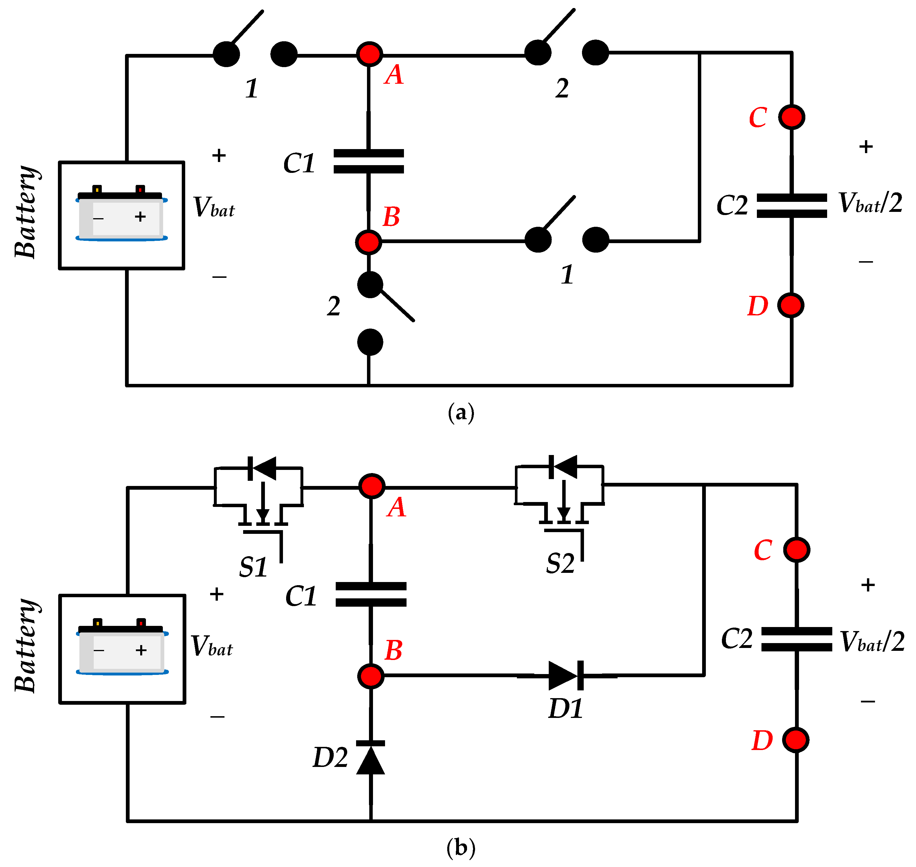
2.3. Voltage Divider Circuit (VDC)

An illustrative example of a switched-capacitor-based buck converter is presented in Figure 8a. As depicted in this figure, two capacitors C1 and C2, each of equal value, are connected in series, resulting in a voltage of Vbat/2 across each capacitor. The capacitors are subsequently rearranged in parallel as the switching sequence progresses, yielding an output voltage of Vbat/2. The switching model employed to achieve this is depicted in Figure 8b, where pairs of switches 1 and 2 operate in reverse-phase order. When the load is active, current flows through the capacitors. However, if the switching frequency is sufficiently high and the capacitors charge within short time intervals, the output voltage remains largely unaffected. Figure 8b showcases a switch-capacitor cell configuration designed to implement the Buck circuit.
Initially, switch S1 is activated while S2 remains without a switching pulse at its gate-source pins. Consequently, a positive voltage applied to the anode pin of diode D1 turns it on, while diode D2 remains in the off state. Since both capacitors have the same value, the input voltage divides evenly across them, as depicted in Figure 9a.
Once both capacitors are adequately charged, switch S1 is deactivated and switch S2 receives the pulse signal, connecting to the circuit. During this switching moment, diode D1 is deactivated and D2 becomes active, establishing a parallel connection between capacitors C1 and C2. This arrangement results in an output voltage that is half of the input voltage source. This state is presented in Figure 9b.

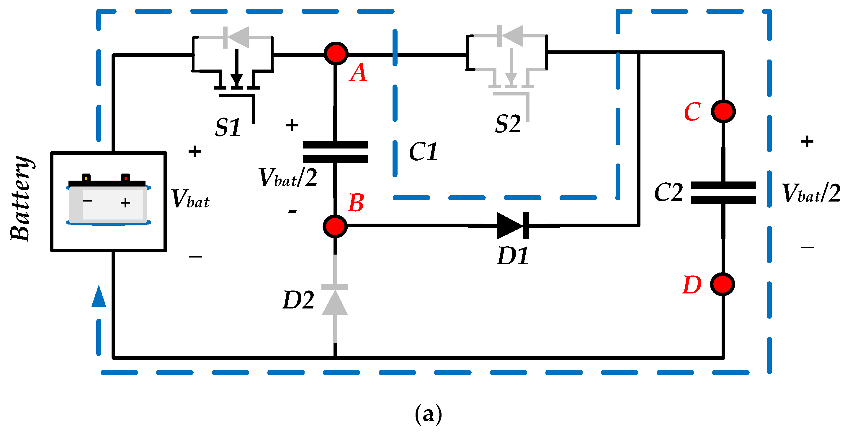
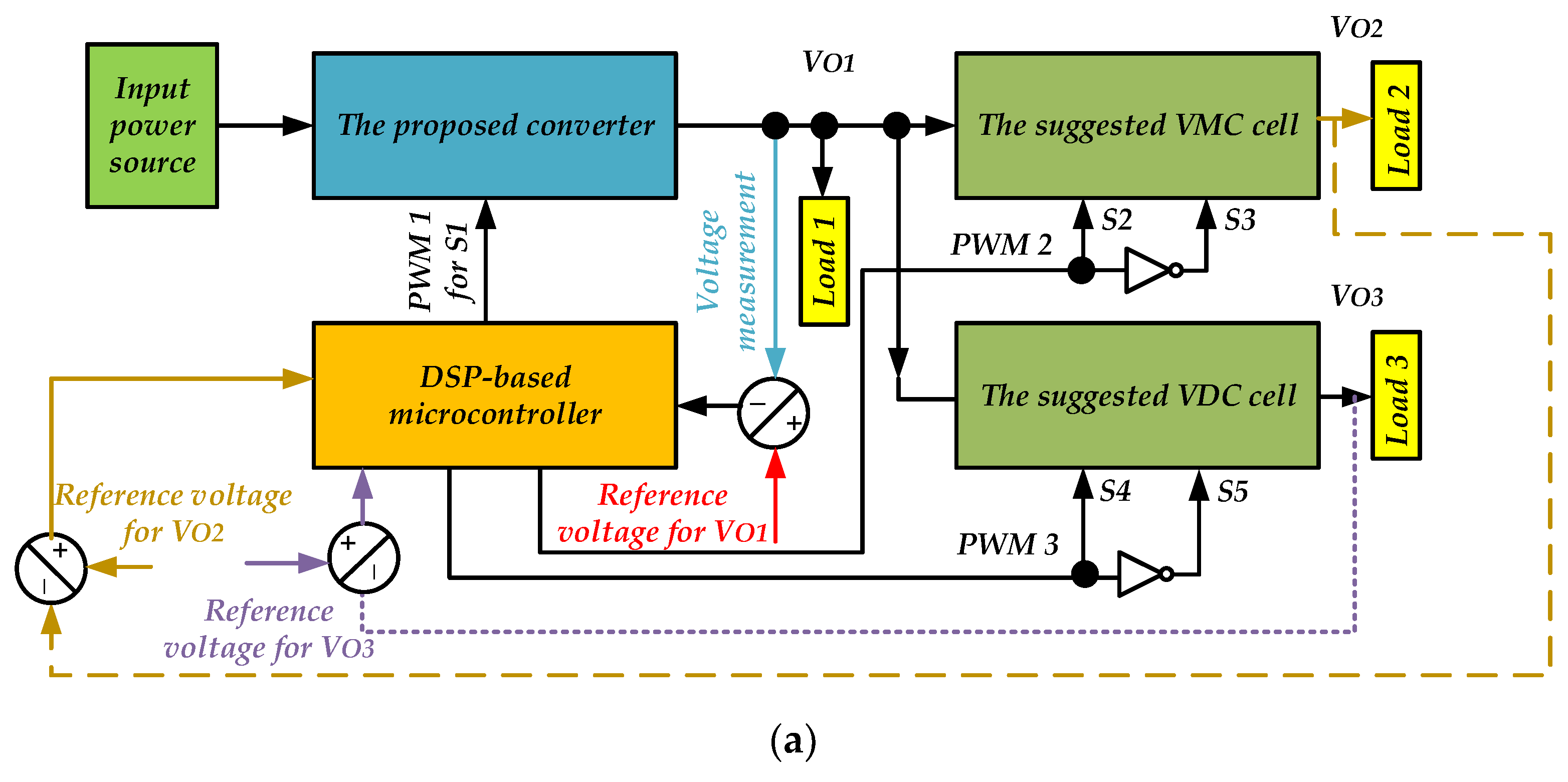
2.4. The Proposed Converter with VMC and VDC Cells

In line with the earlier discussion, it is important to note that EV applications require various DC voltage levels to power different components of the vehicle. Additionally, the power supply for various electronic boards must be derived from the main battery pack. Consequently, the power module of an EV necessitates a configuration that accommodates multiple DC voltage levels. The suggested approach involves the integration of a buck–boost converter with two VMC and VMD converter cells, as illustrated in Figure 10. This converter operates by generating the primary essential voltage at its output nodes, tailored to the band-limited battery voltage. Subsequently, it generates two additional voltages to meet the specific requirements of the vehicle’s driving circuits. It is important to note that this proposed configuration serves as a sample circuit, and we have the flexibility to use either a VMC or VDC cell independently. Furthermore, by cascading these proposed cells, it is possible to generate a greater or lesser number of DC voltage levels as needed. As a result, the proposed converter includes VMC and VDC cells to generate additional DC voltage. This implies that if, for instance, a 24 VDC is produced at Vo1 (X-Y nodes), Vo2 can generate 48 VDC and Vo3 can generate 12 VDC as required for various electric vehicle (EV) circuits. For that and according to the requested voltage of other parts of the EV, such as the headlight, air-conditioning, and wiper systems in EV, VMC or VDC or both can be used by connecting to the X-Y nodes. The operational principles of the VDC and VMC circuits have already been depicted in Figure 6, Figure 7, Figure 8 and Figure 9. Each circuit requires two straightforward PWM switching signals to activate the switches. Additionally, a NOT gate is essential in the switching circuit because only one switch in each circuit should be activated during each time interval. In the VDC circuit, this implies that when switch S2 is turned on, switch S3 must be turned off. This switching sequence is presented by the PWM 2 signal. In the VMC converter, PWM 3 activates switch S4 when switch S5 is turned off, and conversely, PWM 3 deactivates S5 when S4 is activated. The choice of switching frequency typically falls within the range of 10 to 100 kHz and can be tailored according to the characteristics of the switches being used.

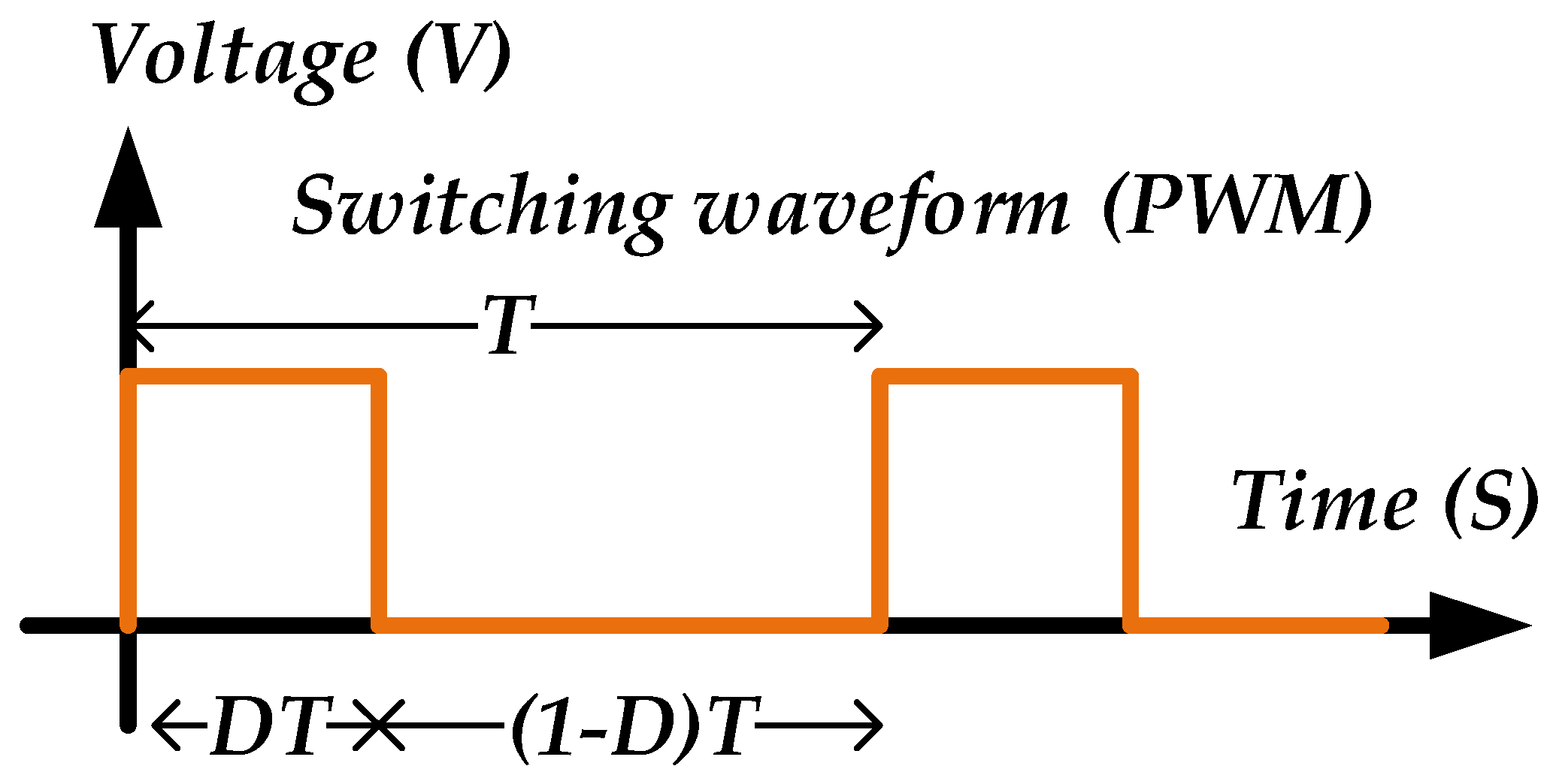
2.5. Control Process

The application of a PID controller in a buck–boost converter for EV systems offers several advantages, including improved transient response, enhanced steady-state accuracy, and adaptability to varying operating conditions. While setting the PID coefficients (Kp, Ki, and Kd) may initially seem complex, modern control design tools, simulations, and systematic tuning methods make the process more accessible, ensuring optimal converter performance in EV applications. The integration of PID control in buck–boost converters contributes to the overall efficiency and reliability of electric vehicles, aligning with the growing demand for sustainable and advanced transportation solutions.
In Figure 10, e ( t ) is the error signal, which is the difference between the desired reference input ( V r e f ) and the actual output voltage ( V o u t ) of the converter at time t:
e t = V r e f V o u t
u ( t ) is the control input to the converter, which is the duty cycle of the converter’s switch at time t . The PID controller can be expressed as:
u t = K p e t + K i 0 t e τ d τ + K d d e ( t ) d t
where K p is the proportional gain, which determines the immediate response of the controller to the current error signal. It scales the error directly and contributes to the control effort in proportion to the current error. K i is the integral gain, which accumulates the error over time and helps eliminate steady-state errors. It integrates the error signal over time, taking into account past errors. K d is the derivative gain, which accounts for the rate of change of the error signal. It provides control action to anticipate future error changes, helping to reduce overshoot and improve system stability. e ( t ) is the error signal, as defined above. 0 t e τ d τ represents the integral of the error signal with respect to time from the initial time (0) to the current time (t), which is the accumulated error, and d e ( t ) d t represents the derivative of the error signal with respect to time, indicating the rate of change of the error.
The goal of the PID controller is to adjust the duty cycle ( u ( t ) ) of the proposed converter’s switch in real time based on the error signal, its integral, and its derivative using the gains ( K p , K i ) and K d to achieve the desired output voltage ( V o u t ) and maintain system stability.

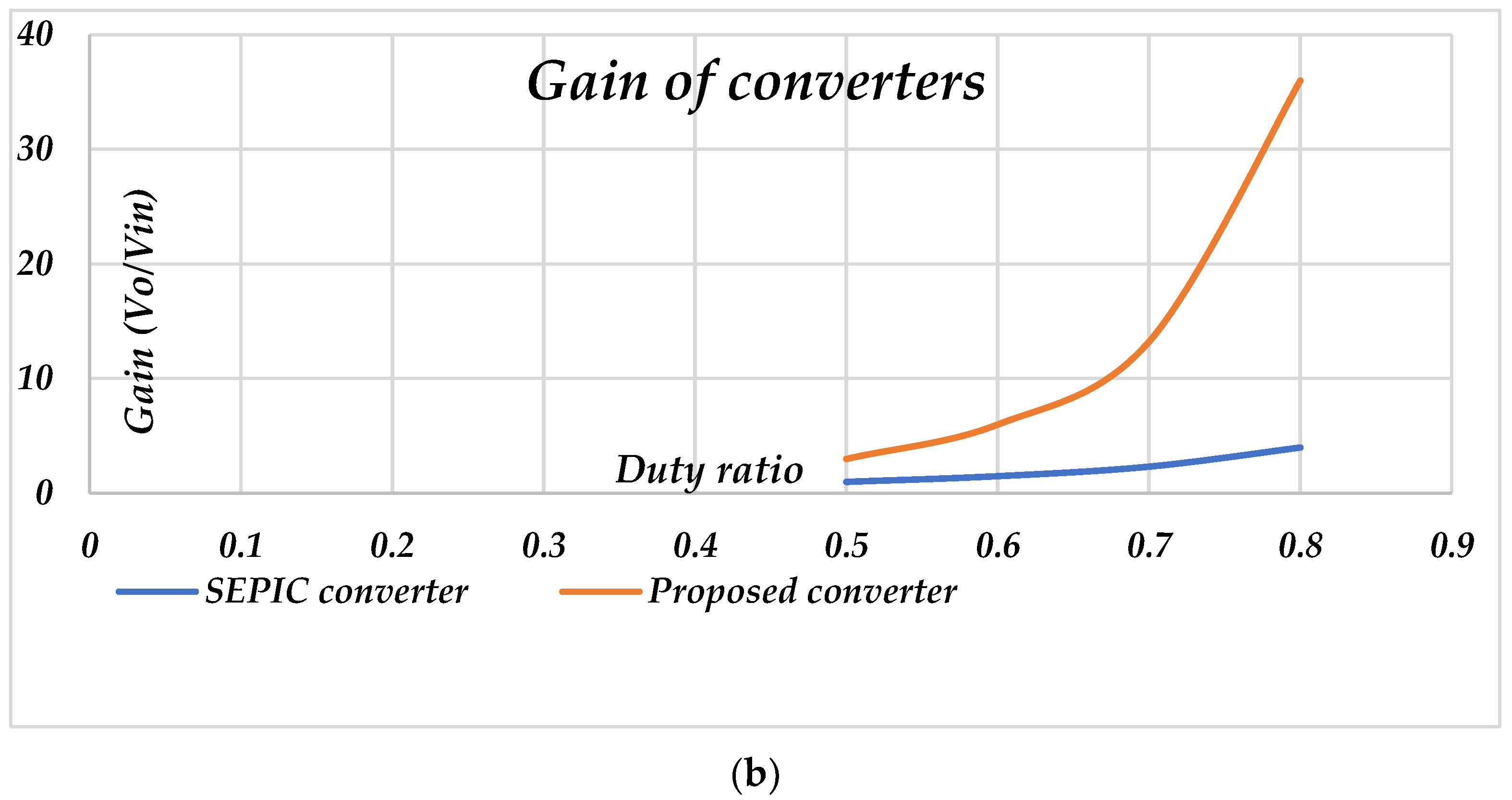
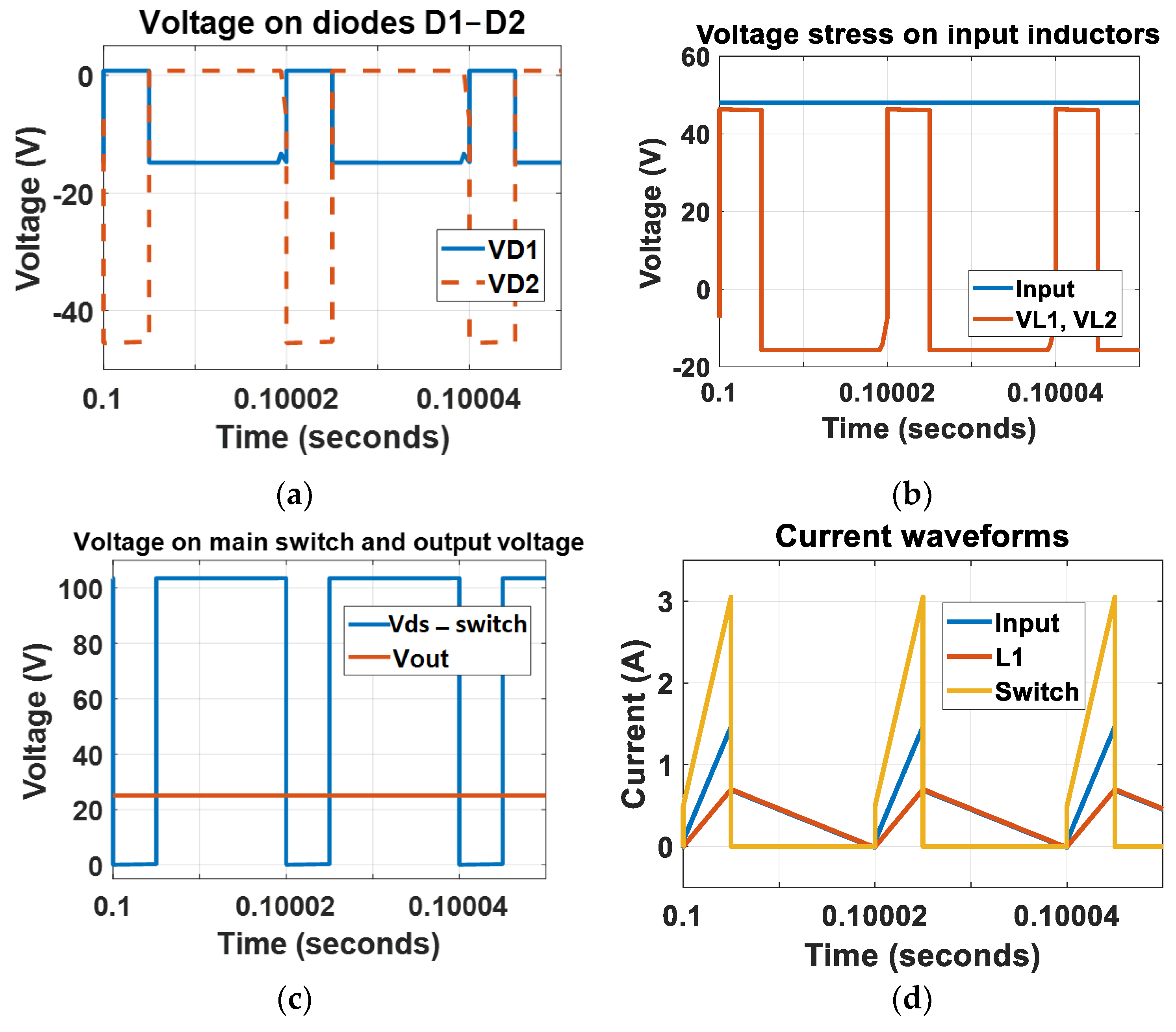
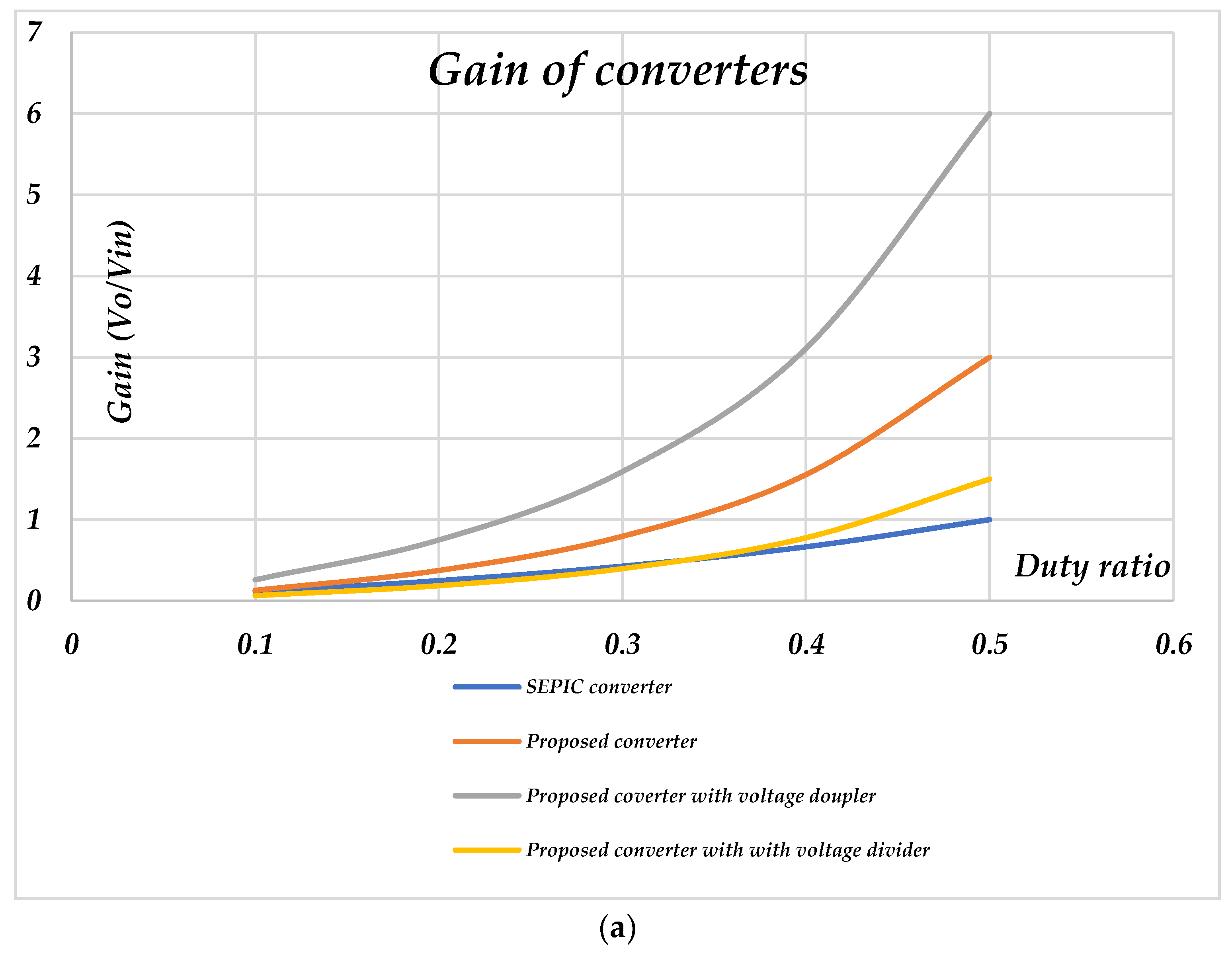
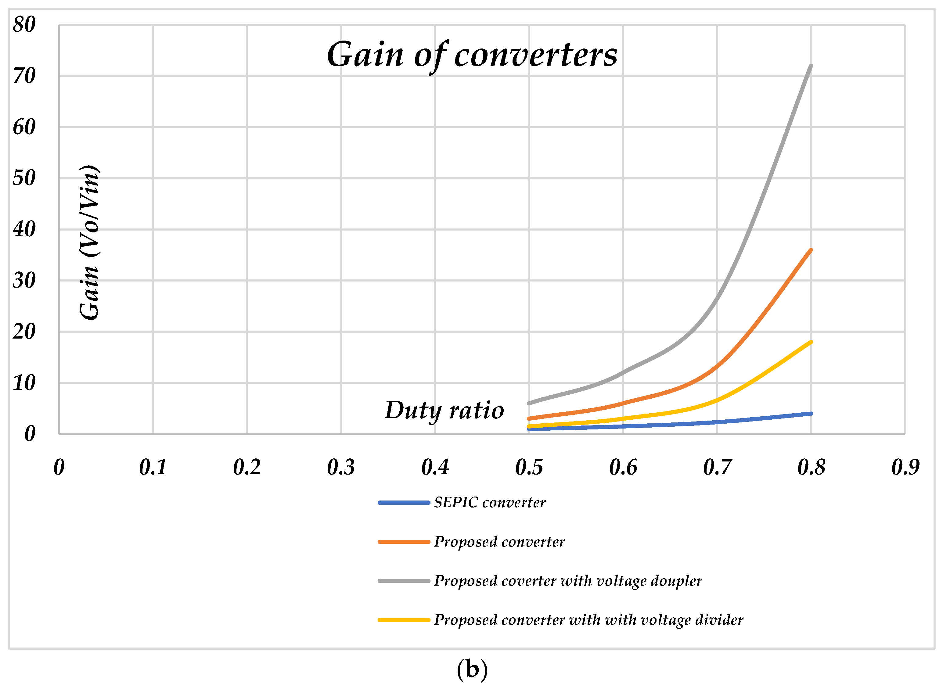
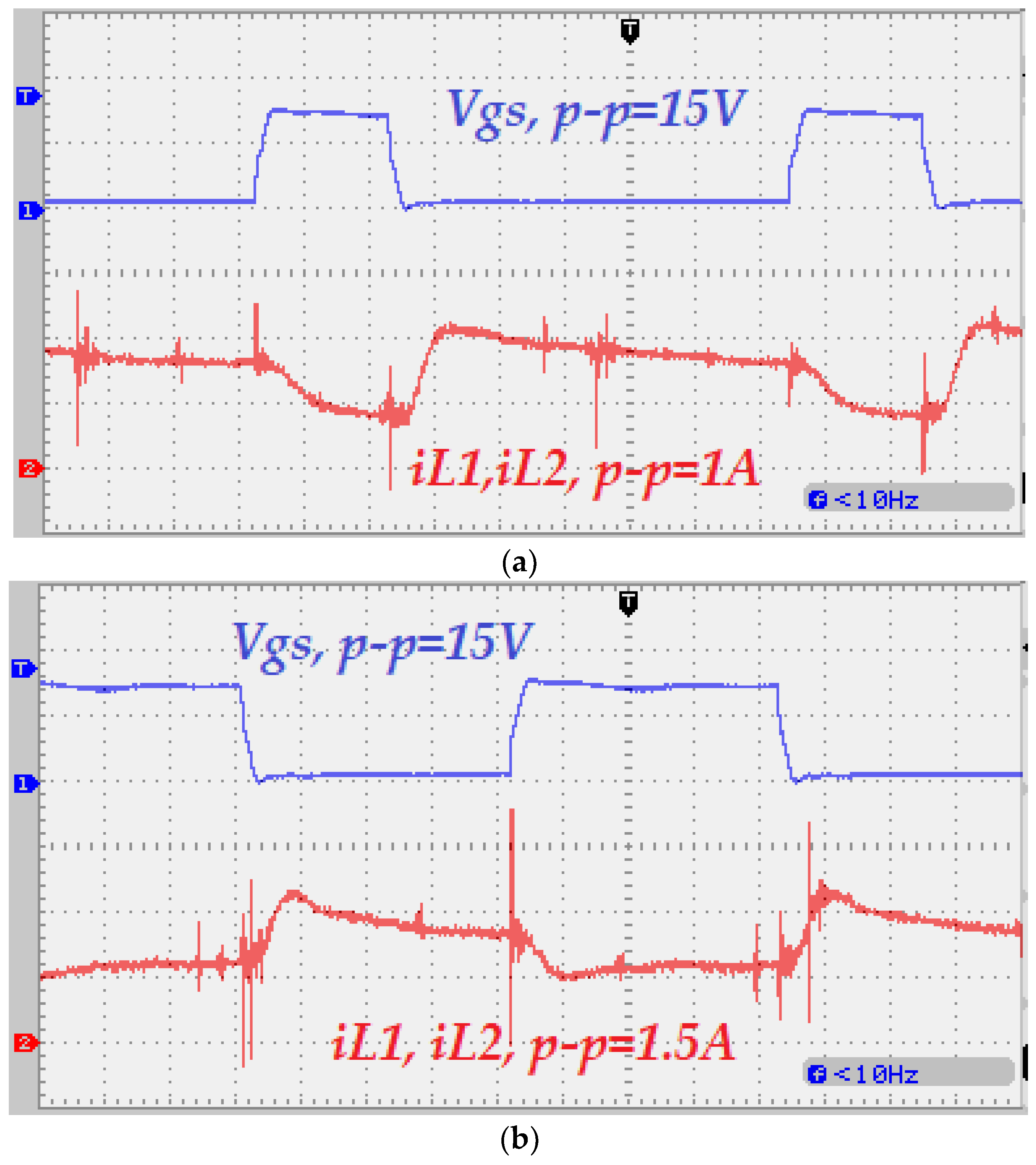
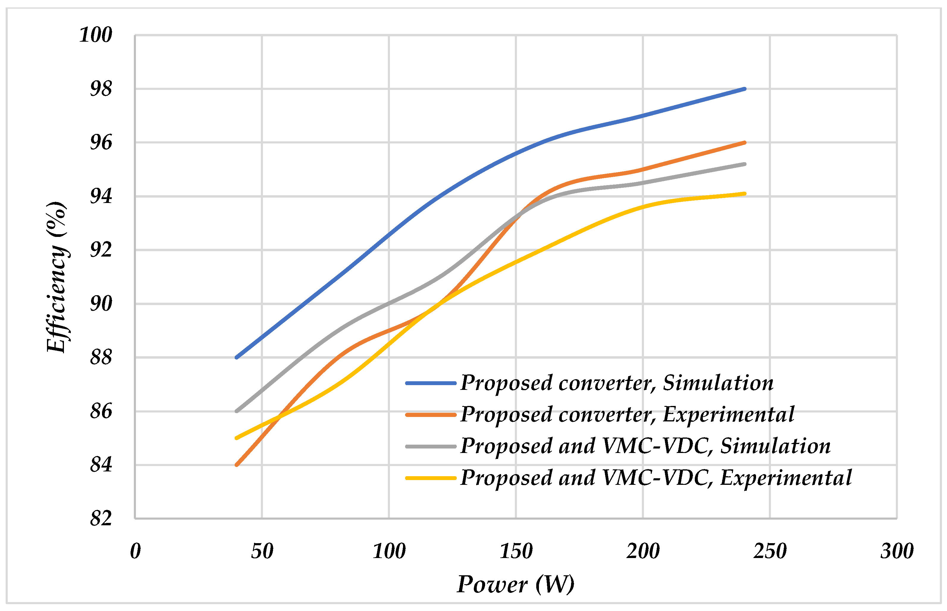
3. Results and Discussion

In the initial stage, the proposed converter underwent simulation testing, and the outcomes are detailed within this section. Subsequently, the corresponding circuit was physically implemented in a laboratory setting, thus validating and corroborating the theoretical and simulated findings.

Simulation Results

Considering Equation (13), the critical duty ratio can be easily calculated as D = 0.33. At this specific D value, the proposed converter exhibits an output voltage equal to that of the input voltage source. As the duty cycle deviates from this critical value, the converter’s behavior changes accordingly. When the duty cycle is shorter, the converter functions as a buck converter, and when it is longer, it transforms into a boost converter. To illustrate these characteristics, Figure 11, Figure 12 and Figure 13 depict varying voltage and current waveforms for the converter components at D = 0.33, D = 0.25, and D = 0.5, respectively. Consequently, Figure 11 is expected to show no change in the output voltage, while Figure 12 should display a lower voltage and Figure 13 is anticipated to exhibit a higher voltage.
For the simulation, a 48 VDC input source was employed, and voltage and current waveforms across various components were recorded. In Figure 11a, the voltage waveforms across diodes D1 and D2 are presented. Theoretically, it has been established that these two diodes should activate asynchronously, and at any given time, only one of them should be conducting. Remarkably, the simulation results align with this theoretical expectation. This pattern remains consistent for different duty ratio values, as evidenced in Figure 12a and Figure 13a. In these figures, it is evident that the maximum voltage across each diode equals the input voltage, and similarly, diode D3 exhibits the same voltage waveform as diode D1.
Moving on to Figure 11b, Figure 12b and Figure 13b, these graphs illustrate the voltage across inductors L1 and L2, as well as the input voltage source. Two significant observations can be made from these figures. Firstly, both input inductors exhibit identical voltage waveforms, indicating that they are charged and discharged concurrently. Secondly, the maximum voltage value across the inductors corresponds to the input voltage source.
Figure 11c, Figure 12c and Figure 13c depict the output voltage achieved for various duty ratios, and they also provide insight into the voltage stress across the switch S1. By analyzing the measured voltages and referencing Equation (13), it becomes evident that the obtained output voltages align with the expected values for the converter. For instance, at D = 0.33, the output voltage matches the input voltage source, while at D = 0.5, the output voltage reaches three times the input voltage. Notably, the voltage stress across the switch increases proportionally with the measured output voltage.
Finally, Figure 11d, Figure 12d and Figure 13d provide a crucial depiction of the current waveforms for various converter elements. These figures illustrate that all key currents in the system, including the input source currents, inductor L1 and L2 currents, and the drain-source pin currents of the switch, exhibit perfect phase alignment. For instance, when the input source current surges, it charges inductors L1 and L2, causing their currents to rise simultaneously. Consequently, the switch is connected, facilitating the transfer of a positive current from the inductors to the switch. Conversely, when the switch is disconnected, the input current diminishes, initiating the discharge of the inductors. Importantly, the currents in the inductors remain continuous, ensuring the converter operates in continuous current mode (CCM).
As a switching duty ratio of D = 0.33 is chosen for the depicted converter in Figure 11, it results in the output nodes generating the same voltage as the input voltage. In this simulation, the input voltage is set at 48 VDC, which causes the output nodes to also produce the same voltage. Specifically, diode D1 exhibits a voltage drop ranging from 0 to −20 V, while diode D2 experiences voltage variations between 0 and −45 V, as illustrated in Figure 11a. For this input voltage, both inductors L1 and L2 exhibit identical switching voltages that oscillate between −22 and 45 VDC, as shown in Figure 11b. Figure 11c displays the generated output voltage and the voltage across the drain-source pins of the main power switch. In this state, the peak drain-source voltage reaches approximately 140 V. Finally, Figure 11d illustrates the current waveforms for the input source, inductor L1, and the power switch. The minimum and maximum current magnitudes for the input source, inductor L1, and the switch vary within the ranges of 0.6 A to 2.9 A, 0.6 A to 1.2 A, and 0 to 5.3 A, respectively.
As previously mentioned, when using a duty ratio of D = 0.25, the proposed converter operates in a manner resembling a buck converter. In this configuration, with a 48 VDC input voltage, a 24 VDC is generated at the load. For this particular condition, the voltage across diode D1 fluctuates between 0 and −15 V, while the voltage across diode D2 oscillates between 0 and −45 V, as depicted in Figure 12a. The switching voltages generated across inductors L1 and L2, ranging from 50 to −18, are visible in Figure 12b. Since the generated output voltage is lower than the input voltage, the voltage across the drain-source terminals of the switch decreases, reaching levels between 0 and 105 V, as shown in Figure 12c. In the context of this buck converter operation, input currents are generally lower than output currents, as confirmed by Figure 12d. Specifically, the input current varies from 0 to 1.5 A, while the currents in inductor L1 and the switch fluctuate between 0 and 0.6 A and 0 to 3 A, respectively.
With a duty ratio of D = 0.5, the proposed converter operates as a boost converter. Consequently, the voltage and current at the output nodes are higher and lower, respectively, than the voltage and current at the input side. These operational modes have been comprehensively documented in Figure 13. In Figure 13a, the voltage across diodes D1 and D2 fluctuates between 0 and 45 V. Figure 13b shows that the voltages across inductors L1 and L2 increase, reaching values spanning from −45 to 45. The output voltage generated is the highest among the three different states evaluated. Consequently, the voltage across the drain-source terminals of the switch also reaches its maximum, peaking at 280 V, as illustrated in Figure 13c.
In this boost converter configuration, the current levels on the input side are higher. The input current and inductor L1 current vary from 2.5 to 6.5 A and 2.5 to 3.5 A, respectively. The current through the switch ranges from 0 to 12 A for this specific state. These current profiles are detailed in Figure 12d.
For the simulation and experimental tests, a resistive variable load in the form of a rheostat with a range of 5 to 100 Ω is employed, keeping the power within 300 W to align with the laboratory’s available power sources.
The graphical representation of the performance enhancement offered by the proposed converter, incorporating VMC and VDC cells, compared to a conventional SEPIC converter is presented in Figure 14. Figure 14a provides the gain curves for the duty cycle range of 0 < D < 0.5, while Figure 14b showcases the results for the duty cycle range of 0.5 < D < 0.8. These figures display the gain curves for a standard SEPIC converter and juxtapose them with the theoretical voltages achieved by the proposed converter, as well as the voltage curves generated by the VMC and VDC cells. Notably, across all duty ratios, the proposed converter consistently exhibits a higher gain than the conventional SEPIC converter. The VMC and VDC cells effectively double and divide the generated DC voltage, contributing to this enhanced performance.
Figure 15a illustrates the integrated topology, which combines the proposed SEPIC converter with VDC and VMC cells. In this configuration, a DC voltage source is linked to the SEPIC converter, and a DSP-based microcontroller, through output voltage sampling and reference voltage comparison, generates precise PWM signals for switch S1. Additionally, the controller produces PWM signals for the VMC and VDC circuits, facilitating the doubling (VO2) and division (VO3) of the voltage generated at the output nodes (VO1) of the SEPIC converter. Figure 15b depicts the setup of the proposed converter’s workbench. This illustration showcases the utilization of a DSP-based microcontroller for the control of the buck–boost converter, accompanied by real-time visualization. The prototype converter has been subjected to rigorous testing, encompassing various duty ratios. These tests encompass the evaluation of the converter’s performance across different operational modes, including buck, boost, and buck–boost.
Figure 16 is provided to illustrate the switching pattern of the primary power switch and its corresponding behavior. To validate this, we conducted experimental tests following the simulation conditions. In this regard, we selected a 48 VDC DC voltage source as the input, and we assessed both the generated output voltages and the voltage stress experienced by the switch.
Figure 16a–c specifically depicts the drain-source voltages produced by the switch for duty cycle values of 0.25, 0.33, and 0.5, respectively. As was theoretically analyzed, when D = 0.25, the proposed converter operates as a buck converter, and according to the results presented in Figure 12c, an estimated voltage with an amplitude of approximately 110 V should be observed. Figure 16a demonstrates that the measured voltage aligns with the simulation results, confirming the theoretical findings.
In Figure 16b, we observe the gate-source and drain-source voltages for the proposed converter when operating at a duty ratio (D) of 0.33. Simulation results suggest that the drain-source pins should register a voltage of approximately 144 V. The data presented in Figure 16b corroborate this expectation, indicating that the proposed converter indeed matches the anticipated voltage. In this operational mode, the converter exhibits a voltage output that aligns with the input source.
Moving on to a longer duty ratio, Figure 16c illustrates the outcomes of this switching mode. As previously mentioned, when operating with duty ratios exceeding 0.33, the proposed converter transforms into a boost converter. In this mode, it is anticipated that the switch will experience a higher voltage due to the increased output voltage. Both the simulation results and Figure 16c confirm this anticipation, with measurements indicating a voltage of around 280 V for the switch in this specific mode.
In Figure 17, we provide an overview of the current behavior in the input inductors L1 and L2 during the time intervals when the switch is both activated and deactivated. This presentation includes two sample duty ratios, namely, D = 0.25 and D = 0.5. The results presented in this figure serve to corroborate the simulation outcomes shown in Figure 12d and Figure 13d.
Specifically, the current waveforms for D = 0.25 and D = 0.5 are illustrated in Figure 17a and Figure 17b, respectively. These waveforms offer a visual representation of the current status in the input inductors under these two duty ratio scenarios, confirming the findings from the earlier simulations.
Figure 18 displays the generated DC voltages at the output of the converter. When operating with a duty cycle (D) of 0.25, the expectation was to achieve a DC voltage of 24 VDC for the primary load. Figure 18a showcases the voltage measurements for the converter while it is operating in buck mode. Additionally, a VDC cell is connected to the output to demonstrate how the generated voltage can be divided. In this setup, a secondary load voltage of 12 V is attained. The application of the VDC cell is also assessed for the D = 0.33 operational mode, as depicted in Figure 18b. In this case, the converter maintains the same 24 VDC output voltage, which is measured at the output nodes of the VDC cell.
Lastly, the generated voltage under boost operational mode is examined, with results presented in Figure 18c. When the proposed buck–boost converter operates in this mode, it produces a voltage of approximately 144 VDC at its output, while the VMC boost cell records a voltage of about 280 VDC. These observations highlight the differences in voltage output between the two configurations.
In Figure 19, we present the efficiency curves for the proposed converter as well as the voltage doubler and divider cells, based on both simulation and laboratory tests. As one might anticipate, the efficiency of the VMC and VDC cells tends to decrease due to the utilization of more semiconductor devices. Additionally, certain unexpected and minor loss factors, which are typically not accounted for in theoretical analyses, become relevant and contribute to lower efficiencies in experimental tests compared to simulation results.
These results reveal that the proposed buck–boost converter achieves approximately 98% and 96% efficiencies for power levels exceeding 250 W. This indicates that the proposed converter is well suited for medium- and high-power applications, demonstrating its practical viability in real-world scenarios.
To calculate accurate switching and dynamic losses by the components of the converter, the authors other publications have been considered. Refs. [6,7,34] present a comprehensive loss calculation through a deep mathematical analysis. The theoretical and simulation loss calculation in Figure 19 is performed according to these references.
The purpose of Table 1 is to provide a performance comparison between the proposed converter and other similar buck–boost converter topologies designed for electric vehicle (EV) applications. In all these configurations, prototype converters have been tested up to 850 W. The efficiency of these converters ranges from 45 to 96 percent, and the total number of components varies from 9 to 13.
The proposed converter, on the other hand, comprises a total of 12 components, excluding the input rectifier circuit. When considering the input rectifier circuit, the total number of power components increases to 16. Notably, the most expensive elements within these converters are the inductors and power switches. However, the proposed converter distinguishes itself by utilizing only one power switch and three inductors. This approach places the overall component cost of this converter at a medium level.
An important advantage of the proposed converter is its minimal number of power switches. This simplicity streamlines the control process and avoids complex control flowcharts and implementations, making it a notable feature of the converter.
The inductors in the proposed converter operate in what is known as continuous conduction mode (CCM), which is an essential requirement in power converters. In contrast, working in a discontinuous current mode (DCM) for an inductor implies that the inductor current drops to zero during certain time intervals, potentially leading to issues with supplying the load current.
By assuming a 12 VDC input voltage source and excluding the VDC and VMC circuits, the proposed converter generates output voltages ranging from 12 to 430 VDC, covering a wide voltage range. With the incorporation of VDC and VMC blocks, this voltage range can be expanded even further, from 6 to 860 VDC. This expanded voltage flexibility represents the second notable feature of the suggested converter.
Additionally, the presented converter exhibits efficiencies ranging from 84 to 96 percent, and it is evident that efficiency increases with higher power levels. This quality positions the converter as well suited for high-power applications, emphasizing its potential for use in such scenarios.
A higher switching frequency is advantageous, as it ensures a smaller converter volume and reduced cost. In Table 1, the various converters are switched at frequencies ranging from 20 to 60 kHz. The proposed converter’s performance at 50 kHz is considered entirely satisfactory and falls within an acceptable range.

4. Conclusions

In the context of electric vehicles (EVs), there is a critical need for different DC voltage levels to power various components. These voltages are typically sourced from a fixed DC voltage supply, such as a battery system. To meet this requirement, power converters are employed to generate the necessary voltages, which can sometimes exceed the battery voltage or be lower than it. Additionally, in EVs, multi-output configurations are crucial, allowing multiple DC voltages to be generated for different loads.
The proposed converter in this study incorporates a switched-inductor cell suggested to minimize input current ripples from the battery pack. It is equipped with two voltage divider and doubler cells, enabling it to provide three different DC voltage outputs in a conventional operational mode. Moreover, by cascading the VDC or VMC cells, even higher DC voltage levels can be generated. The converter’s voltage gain is quite significant. For example, when the input battery voltage is set at 48 VDC with a duty cycle (D) of 0.8, the resulting outputs are substantially amplified, producing voltages 18, 36, and 72 times the input voltage. Conversely, when using a reduced D of 0.2 while maintaining the input voltage at 48 VDC, the converter yields reduced voltages of 0.1875, 0.375, and 0.75 times the initial voltage. This versatility allows for the generation of various DC voltages as needed.
To control the converter, a DSP-based fast-analysis microcontroller is employed. This study presents both theoretical and simulation results, with experimental test results validating the accuracy of the theoretical analysis. This research demonstrates the practical feasibility of the proposed converter in addressing the complex voltage requirements of electric vehicles.

Author Contributions

The distribution of tasks for this study was organized as follows. Conceptualization, D.E.; methodology, D.E.; software, H.T., G.S., E.M. and H.K.; validation, D.E.; formal analysis, H.K. and G.S.; investigation, E.M. and H.K.; writing—original draft preparation, H.T., G.S., E.M. and H.K.; writing—review and editing, D.E.; project administration, G.S. All authors have read and agreed to the published version of the manuscript.

Funding

This study was conducted as part of an industry–university project development agreement established between Bursa Technical University’s Technology Transfer Office and Seger A.Ş. Company (ADTF-2022-005). The project was successfully concluded under the guidance of Associate Professor Davut Ertekin, with the participation of four researchers from Seger AŞ’s R&D department.

Data Availability Statement

Not applicable.

Conflicts of Interest

The authors declare no conflict of interest.

Nomenclature

EVsElectric vehicles
DCDirect current
DSPDigital signal processing
SIMOSingle-input and multi-output
PWMPulse width modulation
EMIElectromagnetic interference
RFIRadiofrequency interference
FLCFuzzy logic controller
MPCModel predictive controller
PIDProportional–integral–derivative
SEPICSingle-ended primary inductance converter
KVLKirchhoff’s voltage law
VMCVoltage multiplier circuit
VDCVoltage divider circuit
CCMContinuous current mode
DCMDiscontinuous current mode

References

  1. Zhang, S.; Li, H.; Duan, S.; Du, X.; Liu, S.; Wang, P.; Zhang, J. A High-Gain DC-DC Converter with a Wide Range of Output Voltage. Electronics 2023, 12, 3498. [Google Scholar] [CrossRef]
  2. Rehman, A.U.; Kim, M.; Jung, J.-W. State-Plane Trajectory-Based Duty Control of a Resonant Bidirectional DC/DC Converter with Balanced Capacitors Stress. Mathematics 2023, 11, 3222. [Google Scholar] [CrossRef]
  3. Ghaderi, D.; Maroti, P.K.; Sanjeevikumar, P.; Holm-Nielsen, J.B.; Hossain, E.; Nayyar, A. A Modified Step-Up Converter with Small Signal Analysis-Based Controller for Renewable Resource Applications. Appl. Sci. 2020, 10, 102. [Google Scholar] [CrossRef]
  4. Khan, M.S.; Nag, S.S.; Das, A.; Yoon, C. Analysis and Control of an Input-Parallel Output-Series Connected Buck-Boost DC–DC Converter for Electric Vehicle Powertrains. IEEE Trans. Transp. Electrif. 2023, 9, 2015–2025. [Google Scholar] [CrossRef]
  5. Sayed, S.S.; Massoud, A.M. Review on State-of-the-Art Unidirectional Non-Isolated Power Factor Correction Converters for Short-/Long-Distance Electric Vehicles. IEEE Access 2022, 10, 11308–11340. [Google Scholar] [CrossRef]
  6. Qiu, Y.; Xu, M.; Yao, K.; Sun, J.; Lee, F.C. Multifrequency Small-Signal Model for Buck and Multiphase Buck Converters. IEEE Trans. Power Electron. 2006, 21, 1185–1192. [Google Scholar] [CrossRef]
  7. Ertekin, D. A high gain switched-inductor-capacitor DC-DC boost converter for photovoltaic-based micro-grid applications. CSEE J. Power Energy Syst. 2023, 125, 1–19. [Google Scholar]
  8. Qi, Q.; Ghaderi, D.; Guerrero, J.M. Guerrero, Sliding mode controller-based switched-capacitor-based high DC gain and low voltage stress DC-DC boost converter for photovoltaic applications. Int. J. Electr. Power Energy Syst. 2021, 125, 106496. [Google Scholar] [CrossRef]
  9. Chandrasekar, B.; Nallaperumal, C.; Padmanaban, S.; Bhaskar, M.S.; Holm-Nielsen, J.B.; Leonowicz, Z.; Masebinu, S.O. Non-Isolated High-Gain Triple Port DC–DC Buck-Boost Converter with Positive Output Voltage for Photovoltaic Applications. IEEE Access 2020, 8, 113649–113666. [Google Scholar] [CrossRef]
  10. Markkassery, S.; Saradagi, A.; Mahindrakar, A.D.; Lakshminarasamma, N.; Pasumarthy, R. Modeling, Design and Control of Non-isolated Single-Input Multi-Output Zeta–Buck–Boost Converter. IEEE Trans. Ind. Appl. 2020, 56, 3904–3918. [Google Scholar] [CrossRef]
  11. Givi, H.; Farjah, E.; Ghanbari, T. A Comprehensive Monitoring System for Online Fault Diagnosis and Aging Detection of Non-Isolated DC–DC Converters’ Components. IEEE Trans. Power Electron. 2019, 34, 6858–6875. [Google Scholar] [CrossRef]
  12. Ahmed, H.F.; Moursi, M.S.E.; Zahawi, B.; Hosani, K.A.; Khan, A.A. Single-Phase Symmetric-Bipolar-Type High-Frequency Isolated Buck-Boost AC–AC Converter with Continuous Input and Output Currents. IEEE Trans. Power Electron. 2021, 36, 11579–11592. [Google Scholar] [CrossRef]
  13. Kim, J.; Ryu, S.W.; Kim, M.; Jung, J.W. Triple-Mode Isolated Resonant Buck–Boost Converter over Wide Input Voltage Range for Residential Applications. IEEE Trans. Ind. Electron. 2021, 68, 11087–11099. [Google Scholar] [CrossRef]
  14. Lu, Y.; Wu, H.; Sun, K.; Xing, Y. A Family of Isolated Buck-Boost Converters Based on Semiactive Rectifiers for High-Output Voltage Applications. IEEE Trans. Power Electron. 2016, 31, 6327–6340. [Google Scholar] [CrossRef]
  15. Kafle, Y.R.; Hasan, S.U.; Town, G.E. Quasi-Z-source based bidirectional DC-DC converter and its control strategy. Chin. J. Electr. Eng. 2019, 5, 1–9. [Google Scholar] [CrossRef]
  16. Zeng, J.; Du, X.; Yang, Z. A Multiport Bidirectional DC–DC Converter for Hybrid Renewable Energy System Integration. IEEE Trans. Power Electron. 2021, 36, 12281–12291. [Google Scholar] [CrossRef]
  17. Li, R.; Shi, F. Control and Optimization of Residential Photovoltaic Power Generation System with High Efficiency Isolated Bidirectional DC–DC Converter. IEEE Access 2019, 7, 116107–116122. [Google Scholar] [CrossRef]
  18. Chen, X.; Pise, A.A.; Batarseh, I. Magnetics-Based Efficiency Optimization for Low Power Cascaded-Buck-Boost Converter. IEEE Trans. Circuits Syst. I Regul. Pap. 2020, 67, 5611–5623. [Google Scholar] [CrossRef]
  19. Pollet, B.; Despesse, G.; Costa, F. A New Non-Isolated Low-Power Inductorless Piezoelectric DC–DC Converter. IEEE Trans. Power Electron. 2019, 34, 11002–11013. [Google Scholar] [CrossRef]
  20. Kothapalli, K.R.; Ramteke, M.R.; Suryawanshi, H.M. ZVS–ZCS High Step-Up/Step-Down Isolated Bidirectional DC–DC Converter for DC Microgrid. IEEE Trans. Power Electron. 2023, 38, 7733–7745. [Google Scholar] [CrossRef]
  21. Hong, T.; Geng, Z.; Qi, K.; Zhao, X.; Ambrosio, J.; Gu, D. A Wide Range Unidirectional Isolated DC-DC Converter for Fuel Cell Electric Vehicles. IEEE Trans. Ind. Electron. 2021, 68, 5932–5943. [Google Scholar] [CrossRef]
  22. Oluwasogo, E.S.; Cha, H.; Nguyen, T.T. Beta-Quasi-Z-Source (β-qZS) DC–DC Converter without Duty Cycle Constraint for Wide Input Voltage Applications. IEEE Trans. Ind. Electron. 2022, 69, 12784–12794. [Google Scholar] [CrossRef]
  23. Wu, H.; Mu, T.; Ge, H.; Xing, Y. Full-Range Soft-Switching-Isolated Buck-Boost Converters with Integrated Interleaved Boost Converter and Phase-Shifted Control. IEEE Trans. Power Electron. 2016, 31, 987–999. [Google Scholar] [CrossRef]
  24. Ghaderi, D. Influences of the Switched-inductor and Switched-capacitor Blocks on the Gain of an Improved Step-up Converter. In Proceedings of the 2020 12th International Conference on Electrical and Electronics Engineering (ELECO), Bursa, Turkey, 26–28 November 2020; pp. 226–232. [Google Scholar]
  25. Sabir, B.; Lu, S.-D.; Liu, H.-D.; Lin, C.-H.; Sarwar, A.; Huang, L.-Y. A Novel Isolated Intelligent Adjustable Buck-Boost Converter with Hill Climbing MPPT Algorithm for Solar Power Systems. Processes 2023, 11, 1010. [Google Scholar] [CrossRef]
  26. Dimitrov, B.; Hayatleh, K.; Barker, S.; Collier, G.; Sharkh, S.; Cruden, A. A Buck-Boost Transformerless DC–DC Converter Based on IGBT Modules for Fast Charge of Electric Vehicles. Electronics 2020, 9, 397. [Google Scholar] [CrossRef]
  27. Zheng, W.; Hu, C.; Zhao, B.; Su, X.-B.; Wang, G.; Hou, X.-W.; Gu, B. A Two-Stage DC/DC Isolated High-Voltage Converter with Zero-Voltage Switching and Zero-Current Switching Applied in Electronic Power Conditioners. Energies 2022, 15, 6378. [Google Scholar] [CrossRef]
  28. Mohammadi, M.R. A Lossless Turn-on Snubber for Reducing Diode Reverse Recovery Losses in Bidirectional Buck/Boost Converter. IEEE Trans. Ind. Electron. 2020, 67, 1396–1399. [Google Scholar] [CrossRef]
  29. Cao, Y.; Bai, Y.; Mitrovic, V.; Fan, B.; Dong, D.; Burgos, R.; Boroyevich, D.; Moorthy, R.K.; Chinthavali, M. A Three-Level Buck–Boost Converter with Planar Coupled Inductor and Common-Mode Noise Suppression. IEEE Trans. Power Electron. 2023, 38, 10483–10500. [Google Scholar] [CrossRef]
  30. Lee, H.-S.; Yun, J.-J. High-Efficiency Bidirectional Buck–Boost Converter for Photovoltaic and Energy Storage Systems in a Smart Grid. IEEE Trans. Power Electron. 2019, 34, 4316–4328. [Google Scholar] [CrossRef]
  31. Singh, A.K.; Mishra, A.K.; Gupta, K.K.; Bhatnagar, P.; Kim, T. An Integrated Converter with Reduced Components for Electric Vehicles Utilizing Solar and Grid Power Sources. IEEE Trans. Transp. Electrif. 2020, 6, 439–452. [Google Scholar] [CrossRef]
  32. Wu, Y.-E.; Tai, C.-H. Novel Bidirectional Isolated DC/DC Converter with High Gain Ratio and Wide Input Voltage for Electric Vehicle Storage Systems. Batteries 2022, 8, 240. [Google Scholar] [CrossRef]
  33. Al Attar, H.; Hamida, M.A.; Ghanes, M.; Taleb, M. Review on Modeling and Control Strategies of DC–DC LLC Converters for Bidirectional Electric Vehicle Charger Applications. Energies 2023, 16, 3946. [Google Scholar] [CrossRef]
  34. Kart, S.; Demir, F.; Kocaarslan, İ.; Genc, N. Increasing PEM fuel cell performance via fuzzy-logic controlled cascaded DC-DC boost converter. Int. J. Hydrogen Energy, 2023, in press. [CrossRef]
  35. Tekin, H.; Bulut, K.; Ertekin, D. A novel switched-capacitor and fuzzy logic-based quadratic boost converter with mitigated voltage stress, applicable for DC micro-grid. Electr. Eng. 2022, 104, 4391–4413. [Google Scholar] [CrossRef]
  36. Bayrak, G.; Ghaderi, D. An improved step-up converter with a developed real-timefuzzy-based MPPT controller for PV-based residential applications. Int. Trans. Electr. Energy Syst. 2019, 29, e12140. [Google Scholar] [CrossRef]
  37. Chelladurai, B.; Sundarabalan, C.K.; Santhanam, S.N.; Guerrero, J.M. Interval Type-2 Fuzzy Logic Controlled Shunt Converter Coupled Novel High-Quality Charging Scheme for Electric Vehicles. IEEE Trans. Ind. Inform. 2021, 17, 6084–6093. [Google Scholar] [CrossRef]
  38. Babes, B.; Mekhilef, S.; Boutaghane, A.; Rahmani, L. Fuzzy Approximation-Based Fractional-Order Nonsingular Terminal Sliding Mode Controller for DC–DC Buck Converters. IEEE Trans. Power Electron. 2022, 37, 2749–2760. [Google Scholar] [CrossRef]
  39. Guler, N.; Biricik, S.; Bayhan, S.; Komurcugil, H. Model Predictive Control of DC–DC SEPIC Converters with Autotuning Weighting Factor. IEEE Trans. Ind. Electron. 2021, 68, 9433–9443. [Google Scholar] [CrossRef]
  40. Karamanakos, P.; Geyer, T.; Manias, S. Direct Model Predictive Current Control Strategy of DC–DC Boost Converters. IEEE J. Emerg. Sel. Top. Power Electron. 2013, 1, 337–346. [Google Scholar] [CrossRef]
  41. Veerachary, M.; Trivedi, A. Linear Matrix Inequality-Based Multivariable Controller Design for Boost Cascaded Charge-Pump-Based Double-Input DC–DC Converter. IEEE Trans. Ind. Appl. 2022, 58, 7515–7528. [Google Scholar] [CrossRef]
  42. Seo, S.-W.; Choi, H.H. Digital Implementation of Fractional Order PID-Type Controller for Boost DC–DC Converter. IEEE Access 2019, 7, 142652–142662. [Google Scholar] [CrossRef]
  43. Kobaku, T.; Jeyasenthil, R.; Sahoo, S.; Dragicevic, T. Experimental Verification of Robust PID Controller Under Feedforward Framework for a Nonminimum Phase DC–DC Boost Converter. IEEE J. Emerg. Sel. Top. Power Electron. 2021, 9, 3373–3383. [Google Scholar] [CrossRef]
  44. Kurnaz Araz, H.; Ertekin, D.; Aydın, M. A PID-Controlled High DC Voltage Gain Switched-Inductor and Switched-Capacitor-Based DC-DC Power Buck-Boost Converter Design for Solar Energy Application. J. Innov. Sci. Eng. 2021, 5, 129–142. [Google Scholar] [CrossRef]
  45. Daniel, W. Hart, Power Electronics; McGraw-Hill: New York, NY, USA, 2011; ISBN 9780071289306, 0071289305. [Google Scholar]
  46. Kushwaha, R.; Singh, B. An Improved Battery Charger for Electric Vehicle with High Power Factor. In Proceedings of the 2018 IEEE Industry Applications Society Annual Meeting (IAS), Portland, OR, USA, 23–27 September 2018; pp. 1–8. [Google Scholar] [CrossRef]
  47. Sharifi, S.; Monfared, M.; Babaei, M. Ferdowsi Rectifiers—Single-Phase Buck-Boost Bridgeless PFC Rectifiers with Low Semiconductor Count. IEEE Trans. Ind. Electron. 2020, 67, 9206–9214. [Google Scholar] [CrossRef]
  48. Praneeth, A.V.J.S.; Williamson, S.S. Modeling, Design, Analysis, and Control of a Nonisolated Universal On-Board Battery Charger for Electric Transportation. IEEE Trans. Transp. Electrif. 2019, 5, 912–924. [Google Scholar] [CrossRef]
  49. Kushwaha, R.; Singh, B. A Power Quality Improved EV Charger with Bridgeless Cuk Converter. IEEE Trans. Ind. Appl. 2019, 55, 5190–5203. [Google Scholar] [CrossRef]
  50. Ananthapadmanabha, B.R.; Maurya, R.; Arya, S.R. Improved Power Quality Switched Inductor Cuk Converter for Battery Charging Applications. IEEE Trans. Power Electron. 2018, 33, 9412–9423. [Google Scholar] [CrossRef]
  51. Gupta, J.; Kushwaha, R.; Singh, B. Improved Power Quality Transformerless Single-Stage Bridgeless Converter Based Charger for Light Electric Vehicles. IEEE Trans. Power Electron. 2021, 36, 7716–7724. [Google Scholar] [CrossRef]
Figure 1. Proposed buck–boost converter.
Electronics 12 04381 g001
Figure 2. Switching time intervals for the proposed buck–boost converter.
Electronics 12 04381 g002
Figure 3. The configuration of the switch-on-state mode of the proposed buck–boost converter.
Electronics 12 04381 g003
Figure 4. The configuration of the switch-off-state mode of the proposed buck–boost converter.
Electronics 12 04381 g004
Figure 5. Comparison of the gain of the proposed and conventional converters for (a) D < 0.5 and (b) D > 0.5.
Electronics 12 04381 g005aElectronics 12 04381 g005b
Figure 6. (a) The general configuration of a VMC cell and (b) a sample switched-capacitor-based cell.
Electronics 12 04381 g006
Figure 7. Operation principle of the VMC cell, when switches (a) S1 and (b) S2 are activated.
Electronics 12 04381 g007
Figure 8. (a) The general configuration of a VDC cell and (b) a sample switched-capacitor-based cell.
Electronics 12 04381 g008
Figure 9. Operation principle of the VMC cell, when the switch (a) S1 and (b) S2 is activated.
Electronics 12 04381 g009aElectronics 12 04381 g009b
Figure 10. The proposed buck–boost converter with VMC and VDC cells.
Electronics 12 04381 g010
Figure 11. The voltage and current of components in D = 0.33. (a) Voltage across the diodes D1 and D2, (b) input voltage and voltage across the input inductors L1and L2, (c) voltage on switch S1 and generated output voltage, and (d) input source, input inductor and switch currents.
Electronics 12 04381 g011
Figure 12. The voltage and current of components in D = 0.25. (a) Voltage across the diodes D1 and D2, (b) input voltage and voltage across the input inductors L1–L2, (c) voltage on switch S1 and generated output voltage, and (d) input source, input inductor and switch currents.
Electronics 12 04381 g012
Figure 13. The voltage and current of components in D = 0.5. (a) Voltage across the diodes D1 and D2, (b) input voltage and voltage across the input inductors L1–L2, (c) voltage on switch S1 and generated output voltage, and (d) input source, input inductor and switch currents.
Electronics 12 04381 g013
Figure 14. Gain of the proposed converter in comparison with SEPIC and conventional buck–boost converters for (a) 0 < D < 0.5 and (b) 0.5 < D < 0.8.
Electronics 12 04381 g014aElectronics 12 04381 g014b
Figure 15. (a) The flowchart and (b) the proposed prototype SEPIC converter implemented in the laboratory.
Electronics 12 04381 g015aElectronics 12 04381 g015b
Figure 16. The presented gate-source and obtained drain-source voltages for the switch for (a) D = 0.25, (b) D = 0.33, and (c) D = 0.5.
Electronics 12 04381 g016
Figure 17. The input inductors L1–L2 currents for (a) D = 0.25, (b) D = 0.5.
Electronics 12 04381 g017
Figure 18. The generated DC voltages by application of VDC and VMC cells for (a) D = 0.25, (b) D = 0.33, and (c) D = 0.5.
Electronics 12 04381 g018
Figure 19. Efficiency curves for the proposed converter and VMC-VDC cells in simulation and experiments.
Electronics 12 04381 g019
Table 1. Comparison between the proposed and other similar buck–boost converters for EV applications.
Compared Buck–Boost ConvertersNum. of InductorsNumber of CapacitorsNumber of SwitchesNumber of DiodesTotal Component NumberOperational StateOutput VoltageEfficiencyCostSwitching Frequency
[46]21249DCM48 V(45–82)% (100–600) WMedium20 kHz
[47]332210DCM48 V(89–94)% (60–300) WMedium60 kHz
[48]222410CCM150–450 V(91–96)% (300–1000) WMedium30 kHz
[49]432413DCM300 V(87–90)% (150–850) WHigh50 kHz
[50]321612CCM48 V(78–84)% (200–850) WMedium25 kHz
[51]321612CCM48 V(78–84)% (200–850) WMedium25 kHz
Proposed3216 + 4 (for rectifier)12 + 4CCM12–430 V (Vin = 12 V and maximum D = 0.8)(84–96) %
(50–300) V
Medium50 kHz
Disclaimer/Publisher’s Note: The statements, opinions and data contained in all publications are solely those of the individual author(s) and contributor(s) and not of MDPI and/or the editor(s). MDPI and/or the editor(s) disclaim responsibility for any injury to people or property resulting from any ideas, methods, instructions or products referred to in the content.

