Article

Active Thermal Control in Neutral-Point-Clamped Multilevel Converters Based on Switching-Cell Arrays

by
Salvador Alepuz
1,
Joan Nicolás-Apruzzese
2,*,
Roya Rafiezadeh
2,
Sergio Busquets-Monge
2,
Mariana Raya
3 and
Àlber Filbà-Martínez
4
1
Tecnocampus, Universitat Pompeu Fabra, 08032 Mataró, Spain
2
Universitat Politècnica de Catalunya, 08028 Barcelona, Spain
3
Centro Nacional de Microelectrónica, 08193 Bellaterra, Spain
4
Institut de Recerca en Energia de Catalunya, 08930 Sant Adrià del Besòs, Spain
*
Author to whom correspondence should be addressed.
Electronics 2023, 12(19), 4055; https://doi.org/10.3390/electronics12194055
Submission received: 19 July 2023 / Revised: 15 September 2023 / Accepted: 22 September 2023 / Published: 27 September 2023

Abstract

:
Neutral-point-clamped multilevel converters are a suitable solution to the implementation of low–medium voltage and power applications at present, thanks to their intrinsic superior voltage and current quality. The conventional configurations of these converters present uneven power loss distribution, causing thermal stress in some power semiconductors, which weakens the power converter reliability. To overcome this, an implementation of the neutral-point-clamped multilevel converter based on a switching-cell array is introduced, adding redundant conduction paths on one side and more options to distribute the switching losses on the other side. An active thermal control is proposed to balance the temperature distribution in the converter. A four-level converter has been implemented to evaluate the proposed solution. The experimental results show that the proposed implementation and active thermal control presents an enhanced temperature distribution in the converter and, therefore, reduced thermal stress and better reliability.

1. Introduction

The neutral-point-clamped (NPC) multilevel converter [1] is currently a well-established topology for many applications, such as motor drives [2], wind power generation [3], photovoltaic systems [4], STATCOM [5] and very low-power dc–dc conversion [6], within a wide range of power and voltage ratings. The benefits and drawbacks of NPC multilevel converters have been widely reported in the literature [7,8].
NPC multilevel converters can be built with a full semiconductor layout, since the required, single, common dc voltage source can be implemented with capacitors placed outside the converter legs. Thus, no passive components, usually bulky, are placed inside the converter legs, which helps to achieve a more compact implementation of the converter, leading to a volume reduction and power density increase. This feature is particularly interesting for low–medium-voltage and -power applications, where NPC multilevel converters are suitable thanks to their intrinsic superior voltage and current quality. It is worth highlighting that the capacitor voltages can be kept balanced in all operating conditions for any number of levels [9]. Moreover, the independent control of each dc–neutral point current, and eventually each capacitor voltage or battery current, can be achieved [9], allowing for the converter to operate under unbalanced conditions, which improves the operation of systems such as photovoltaic power generation systems [10] or electric vehicles [11].
In low–medium-voltage and -power applications, converters are typically required to be compact, to save overall volume. The converter’s compactness does not generally help to evacuate the heat generated by the power losses in the converter semiconductors. Hence, thermal issues (amount of power loss, power losses’ distribution and evacuation) must be carefully analyzed.
The reliability of power electronics systems is a major concern [12,13], since an unexpected, sudden, full-system shutdown caused by a power-converter failure is not acceptable in some applications. Power semiconductors are the elements that tend to fail most frequently in the power converter [14]. It is well-known that the reliability of power semiconductors depends strongly on the thermal stresses [13,15]. A high mean semiconductor junction temperature and a high semiconductor junction temperature swing in thermal cycles are the main factors that cause thermal stress. Therefore, it is necessary to reduce thermal stress in the power semiconductors to enhance the power converter’s reliability.
Active thermal control can be defined as the set of control or software techniques used to reduce the thermal stress [16], which are mainly focused on sharing the power losses between paralleled devices and modifying the power loss distribution in the converter. To take advantage of these techniques, it is required that the power converter has redundant switching states and current paths. Since NPC multilevel converters meet this requirement, they are well-suited to active thermal control.
Different topologies can be used to implement NPC multilevel converters. The diode-clamped topology presents an uneven loss distribution, which can be improved using the active-clamped topology (ANPC) [17]. An interesting active thermal control for the active-clamped topology is presented in [17,18]. However, the type and number of redundancies in the topology limits its capacity to balance the loss distribution.
One way to increase the redundancies is to implement the NPC multilevel converter using the switching-cell array (SCA) design approach [19]. The SCA consists of a matrix arrangement of switching cells (SC) that can be configured to implement converter legs. Each SC is realized with a controlled switch, an antiparallel diode and a self-powered gate driver.
The implementation of the NPC multilevel converter using SCA provides several additional redundancies, in comparison with the conventional active-clamped implementation, although these are obtained at the expense of increasing the number of power semiconductor devices in the converter and the control complexity. Since this implementation leads to a higher number of redundancies, the active thermal control will have more available options to distribute the losses, and hence to improve the converter loss distribution to reduce the temperature in the power devices, which will enhance the converter reliability.
In this work, the thermal behavior of a four-level NPC converter has been experimentally tested. Results were obtained for the conventional ANPC topology and for two different proposed implementations for the ANPC topology based on the SCA design approach. In the three analyzed cases, an active thermal control was implemented with the objective of balancing the temperatures of the power semiconductors in the converter as well as possible. The converters were implemented with MOSFETs to take advantage of the SCA design approach, since they are intended for low–medium-power and -voltage applications. Experimental results were analyzed with regard to the thermal balance.
This paper is organized as follows. Section 2 details the NPC multilevel converter’s implementation based on the SCA design approach, including the converter configuration description, the selection of redundant configurations, and an analysis of the conduction and switching losses. Section 3 presents the active thermal control method used in this work. The experimental results, with a comparison of the thermal behavior of the three analyzed configurations, are found in Section 4. A conclusion is then formulated in Section 5.

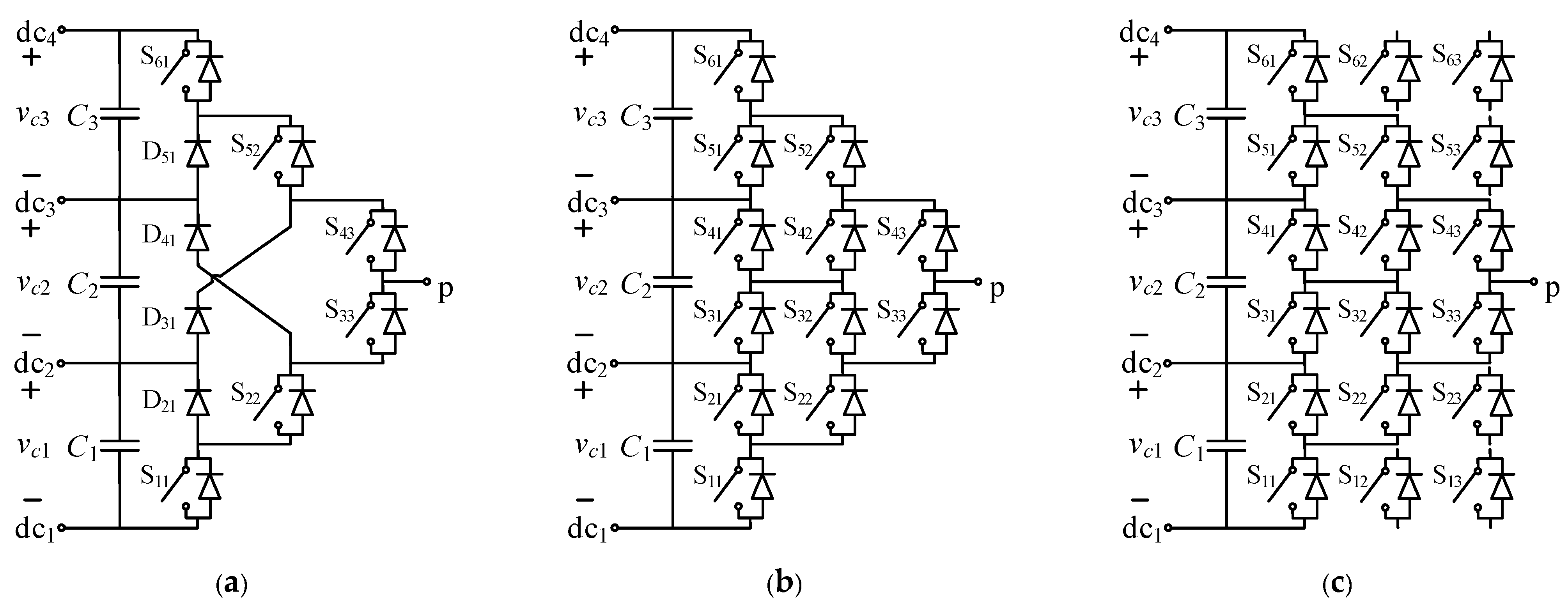
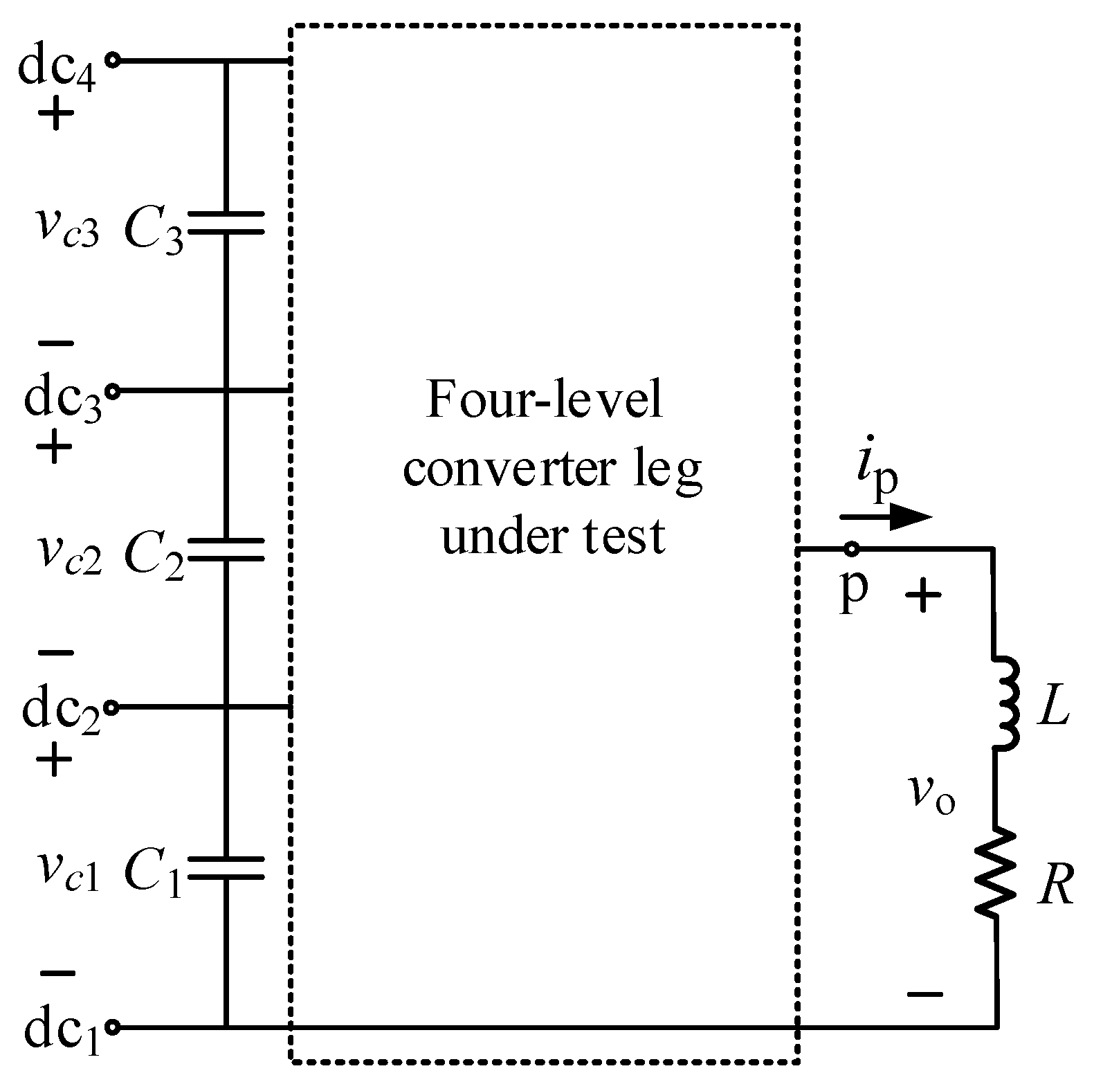
2. Description of the NPC Multilevel Converter Based on SCA

2.1. Topology and Configuration Description

Figure 1 shows three different configurations to implement a four-level NPC converter leg. Although a four-level NPC converter has been considered in this work, the concept can be extended to any number of levels.
In Figure 1, from left to right, it is shown that a greater number of SCs leads to an increase in redundancies in the topology and, hence, more options to distribute the power losses. From the diode-clamped topology in Figure 1a to the active-clamped topology in Figure 1b, the benefits given by the additional redundancies have been described in [17,18,20].
Starting from the active-clamped topology in Figure 1b, six additional SCs (12, 13, 23, 53, 62 and 63) are added to obtain the ANPC topology based on the SCA design approach in Figure 1c, which are not essential for the converter operation. These redundant SCs are represented in Figure 1c without any connection to the converter, since they can be connected in parallel to any of the other SCs, introducing additional degrees of freedom. It is obvious that different configurations can be used to connect these redundant SCs. The present work intends to select the configurations that provide a better power loss distribution among the SCs.

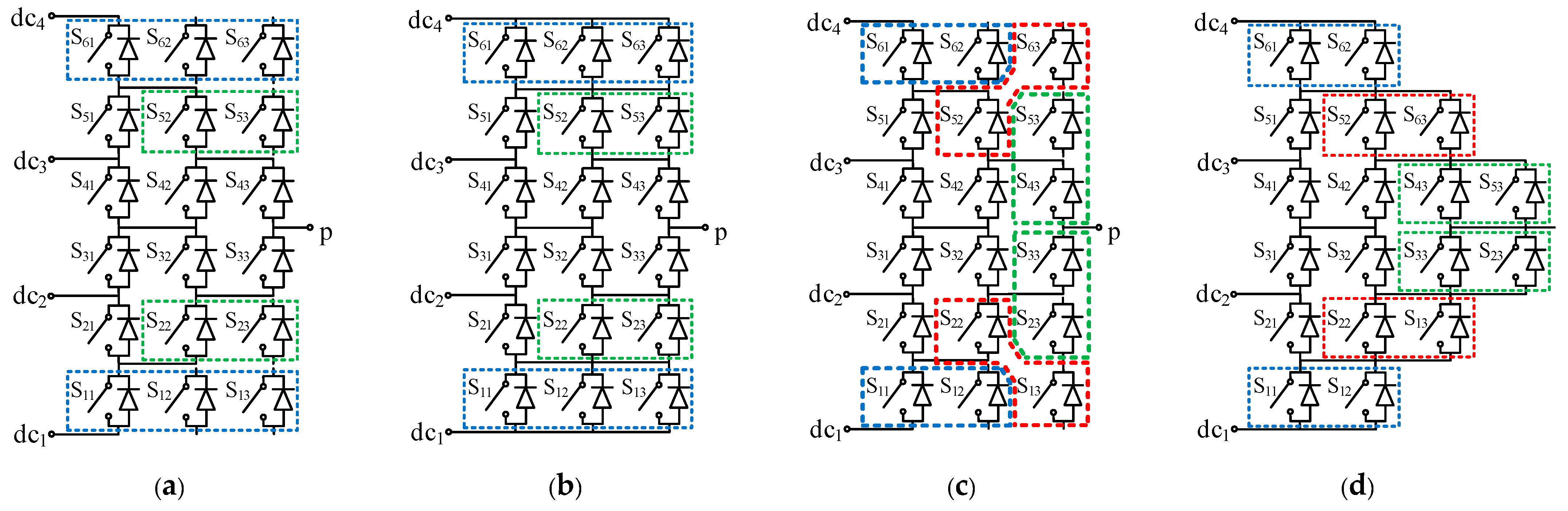
2.2. Selection of Redundant SCA Configurations

For the NPC and ANPC topologies, the power losses of a specific SC depend on the position of the SC in the converter topology [17,18,20].
For instance, in the NPC and ANPC topologies, the upper and lower positions of the SCs in the leg (11 and 61 positions in Figure 1a,b) do not have redundant SCs to share the switching losses, particularly when they are connected to level 1 (position 11) and level 4 (position 61). Therefore, these positions always suffer full switching losses and tend to heat up more than other SCs in the converter.
Regarding the conduction losses, positions 33 and 43 in Figure 1a,b withstand important conduction losses, since these positions conduct all the leg output current, whatever dc level is connected to the output.
That is, in general, the outer diagonals in the NPC and ANPC topologies (positions 11, 22, 33 and 43, 52, 61) are not redundant and either have no options or have very limited options to share their switching or conduction losses, leading to a higher SC temperature. Therefore, it seems reasonable that the additional redundant SCs provided by the SCA design approach will be connected in parallel to these SCs to introduce new redundancies that allow for the sharing of the switching and conduction losses to reduce the temperature of these SCs.
Considering the SCA in Figure 1c and the guidelines provided in the paragraph above, Figure 2 details the two simple and suitable proposed configurations for the connection of the redundant SCs. These configurations have been compared to the conventional ANPC configuration. Note that the physical layout of the converter leg is maintained for all configurations; that is, the spatial position of each SC is always the same as that depicted in Figure 1c, and only the connections of the redundant SCs change.

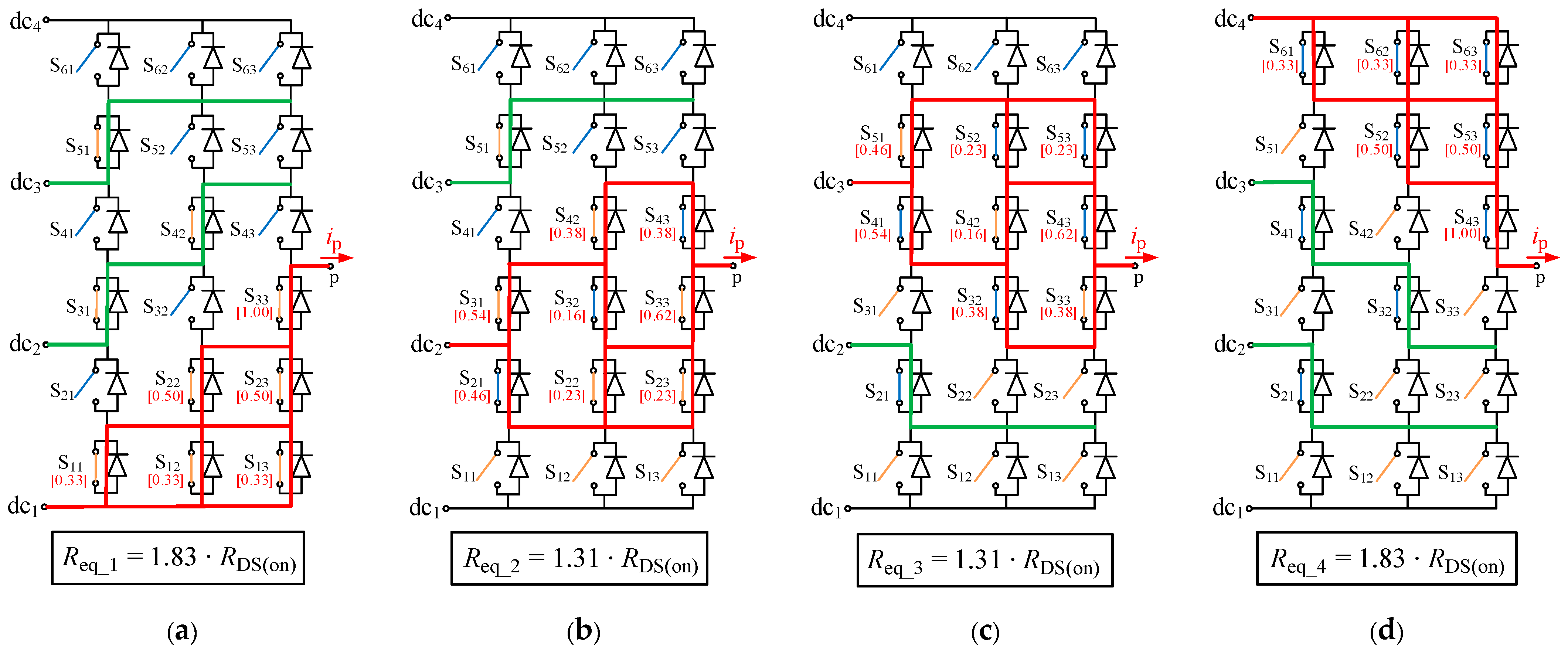
2.3. Switching States: Conduction Losses

As an example, an estimation of the conduction losses for configuration #1 is depicted in Figure 3. The same procedure is applied to the ANPC and configuration #2 to compare the three configurations with respect to the conduction losses.
Figure 3 presents the distribution of the pole terminal current ip for the connection to all dc-input terminals. Red lines indicate the paths followed by the pole terminal current ip and green lines indicate the connections enforced by the switches that guarantee a proper blocking voltage of the devices. In this work, the converter is implemented with power MOSFETs. Thus, the SCs in the on state are represented by the on-state ohmic resistance RDS(ON) of the MOSFET.
In Figure 3, cij_k (in red color within brackets) is the coefficient that presents the per-unit value of the total leg pole terminal current that circulates through the SC Sij when the pole terminal is connected to the dc-input terminal dck.
The conduction power losses per SC in a general n-level leg during a switching period Ts can be calculated as
P cond , S i , j = R DS on T s   ·   k = 1 n 0 d k T s ( c i j _ k ·   i p )   2   ·   d t ,
where dk is the duty ratio of connection of the pole terminal to the dc-input terminal dck. Therefore, the reduction in cij_k will reduce the conduction losses in the respective SC.
In Figure 3, Req_k is the equivalent on-resistance between the pole terminal and input terminal dck, which can be calculated as
R eq _ k = r k · R DS on ,
where rk is the proportionality coefficient resulting from the specific configuration for the connection to the corresponding dc-input terminal dck.
Thus, the conduction losses in a general n-level leg can be calculated as
P cond , leg = k = 1 n R eq _ k T s   ·   0 d k T s i p   2   ·   d t ,
from which it can be deduced that a reduction in rk will produce a reduction in the converter leg conduction losses.
Table 1 shows the coefficients cij_k for all the SCs of the three considered configurations. In the ANPC configuration, positions 61-52-43 have cij_k = 1 for k = 4, as positions 33-22-11 for k = 1, and concentrate the conduction losses. Configuration #1 spreads the conduction losses in these positions, and reduces cij_k, except for the non-redundant positions 33 and 43, which still have cij_k = 1 for both k = 1 and k = 4. Positions 11-12-13 and 61-62-63 lead to the best reduction, since there are three positions in parallel. Configuration #2 presents the most balanced conduction loss distribution for the three analyzed configurations, since the highest cij_k for any SC is 0.52.
As shown in Table 2, the resistance proportionality coefficient rk reduces from the ANPC to configuration #2 for all connections to any dc-input terminal dck, leading to a reduction in the leg conduction losses.
From the conduction loss perspective, configuration #2 leads to the best performance, since the leg conduction losses are the lowest, and provides the best conduction loss distribution among the SCs.

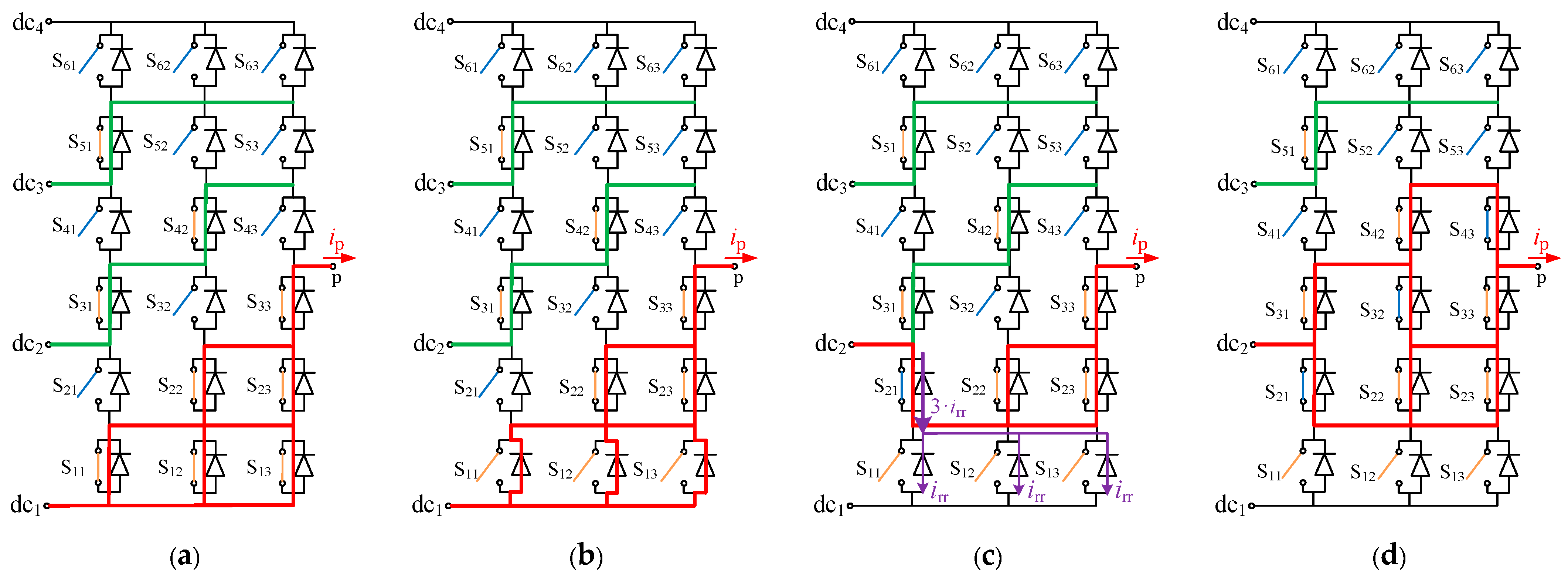
2.4. Switching Transitions: Switching Losses

In the considered converter configurations, the output leg pole terminal switching transitions always occur between adjacent dc-input levels. As an example, Figure 4 illustrates the switching losses for the transition of the output leg pole terminal from dc-input terminal dc1 to dc-input terminal dc2 for configuration #1, where the pole terminal current is assumed to be positive (ip > 0). The same procedure is applied to all the transitions in the three converter configurations considered, to make a comparison with respect to the switching losses. A detailed description of the switching losses in ANPC legs is found in [21], which can be extended to all the configurations considered in the present work.
Figure 4a shows the initial switching state, in which the leg pole terminal is connected to the dc-input terminal dc1. To switch from dc1 to dc2, the SCs 11-12-13 are turned off and 21-32-43 are turned on, but a procedure must be followed to assign the switching losses to a specific position. In the first step, as shown in Figure 4b, the SCs 11-12-13 are turned off, although this has no practical effect, since the positive pole terminal current flows through the respective antiparallel diodes of the SCs so that the leg pole terminal is still connected to dc1. After a dead time, only one of all the SCs that need to be turned on (21-32-43) is turned on. In this example, the SC 21 is turned on first, as shown in Figure 4c; therefore, the pole terminal current flows through this SC, effectively connecting the leg pole terminal to the dc-input terminal dc2. Finally, after another dead time, the rest of the SCs are turned on, SCs 32-43 in this case (see Figure 4d), finalizing the switching procedure.
The switching losses concentrate on the first SC that is turned on (SC 21). Moreover, as SC 21 is turned on, the antiparallel diodes of SCs 11-12-13 present a reverse-recovery process, as shown in Figure 4c, where the reverse-recovery currents flow through SC 21, leading to an increase in switching loss. Once SC 21 is in the on-state, the voltage across the terminals of the rest of the involved SCs (SCs 32-43) is the small voltage drop in SC 21, since SCs 21-32-43 are connected in parallel, as shown in Figure 4c. Thus, SCs 32-43 are turned on with nearly zero voltage, resulting in negligible switching losses. Notice that, in this example, in each commutation, the switching losses can be assigned to SC 21, 32 or 43, depending on which SC is turned on first.
Figure 4 illustrates a case in which the switching losses are present in the first SC to be turned on. However, in other cases, the switching losses appear in the turn-off commutation. In this case, the switching losses are assigned to the last SC that is turned off, with a similar procedure as that detailed in Figure 4.
Table 3 presents the SCs that can present switching losses and the type of commutation in which the switching losses occur (turn on/turn off) for the three different four-level leg configurations considered in this work as a function of the dc-level switching transition and the pole terminal current direction. With the switching procedure detailed above, at every dc-level switching transition, only one SC presents switching losses and, eventually, some diodes present a reverse recovery. For each leg configuration, dc-level switching transition, and pole terminal current direction, there is a set of available SCs where switching losses can be assigned. Therefore, when a dc-level switching transition occurs, a degree of freedom can be used to assign the switching losses to a specific SC belonging to the corresponding set of available SCs. This assignment can be reconsidered every dc-level switching transition. In contrast, some dc-level switching transitions involve diodes with reverse recovery, whose losses cannot be distributed.
Finally, it is worth highlighting that each leg configuration offers different redundancies and, therefore, different options to distribute the switching losses.

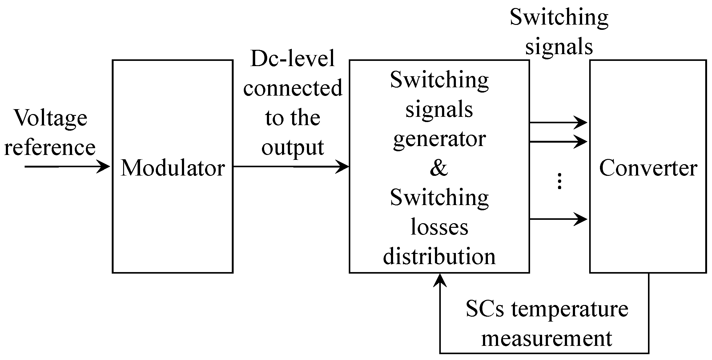
3. Active Thermal Control Method

In this work, the main objective is that the temperature of all SCs in the converter leg is as low and uniform as possible. This goal can be pursued by distributing the power losses evenly among the SCs.
From the description of the losses given in the preceding section, conduction losses depend on the converter leg configuration used, but they cannot be distributed. Instead, switching losses can be effectively distributed. As shown in Table 3, for each configuration and every dc-level switching transition, switching losses can be assigned to a different SC. Thus, switching loss distribution is achieved by varying the switching losses’ assignation over time. Active thermal control is intended to improve the loss distribution, but it does not affect the total amount of loss for each converter leg configuration.
The block diagram of the active thermal control used in this work is depicted in Figure 5. The modulator block indicates the dc-level that is to be connected to the output leg pole terminal. With this information, the switching signals are generated and sent to each SC in the converter. The temperature is measured in every SC of the converter leg. As detailed in Table 3, every dc-level switching transition has an associated set of SCs to which the switching losses can be assigned. The switching loss distribution is achieved by assigning the switching losses to the coldest SC within a set of SCs corresponding to a specific dc-level switching transition. As an example, as shown in Table 3, for configuration #1, with a negative pole terminal current (ip < 0), for the dc-level transition from level 4 to level 3, there is a set of three SCs to which the switching losses can be assigned (51, 42 or 33). The switching losses are assigned to the coldest of these SCs: 51, 42 or 33. Since the temperature of the SCs can vary over time, this active thermal control guarantees that the switching losses will be always assigned to the coldest SC within the available set of SCs in every dc-level switching transition, contributing to the distribution of the losses and the temperature reduction in the hottest cells. However, in this example, positions 61-62-63 present a small amount of switching loss because of the reverse recovery effect of the diodes, which cannot be distributed. It is important to highlight that only the switching losses are distributed among the corresponding devices. Conduction losses are not distributed among the devices.
The active thermal control used in this work achieves a steady-state operation when the temperatures of the available set of SCs in every dc-level switching transition are balanced or, at least, the maximum approximation of this balance is achieved. In practical terms, this means that the switching losses will be distributed over time, in some percentage (given a sufficiently long period of time), among the available set of SCs in every dc-level switching transition. The experimental results in the next section will show the distribution percentages of the switching losses.

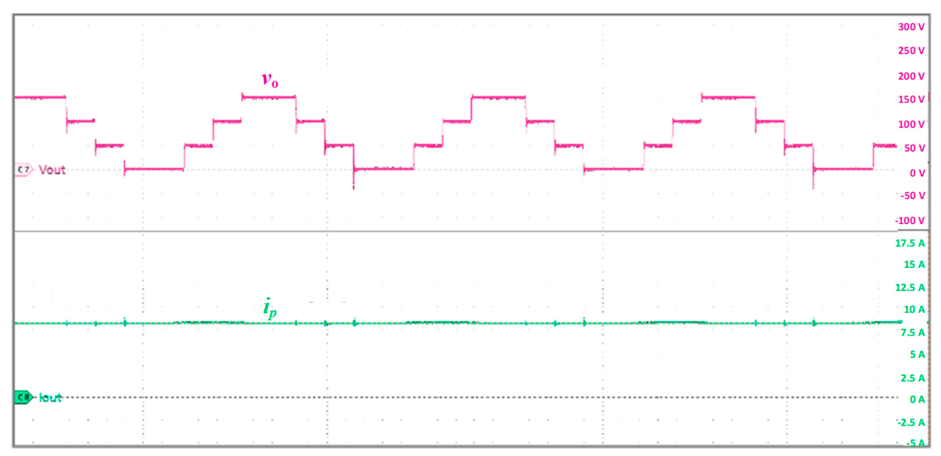
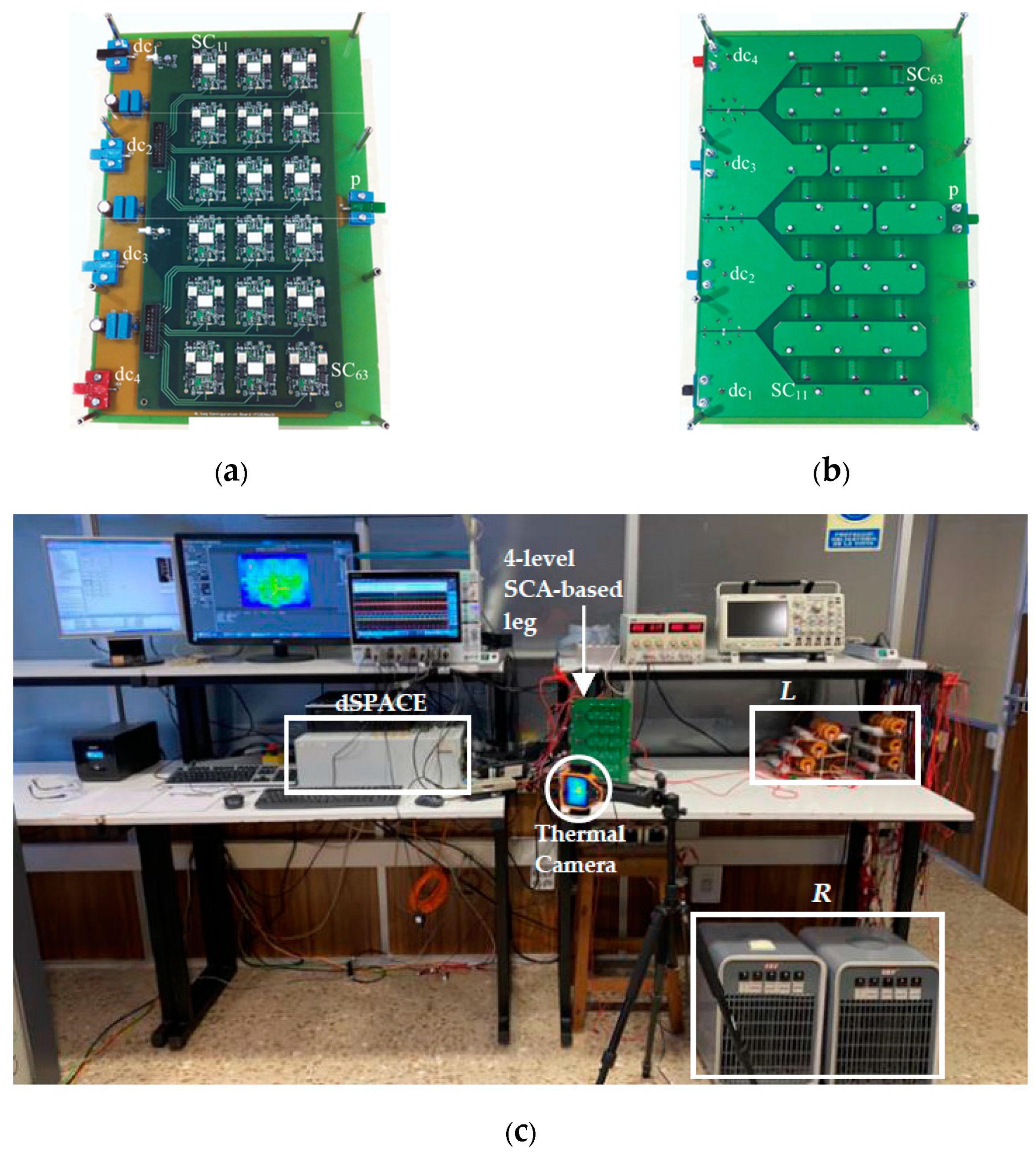
4. Experimental Results

The four-level SCA-based leg was subjected to experimental tests to evaluate the thermal behavior of three different previously presented configurations: ANPC, configuration #1 and configuration #2. The leg was operated as a dc–dc power converter, as shown in Figure 6, by using 50 V dc power supplies across adjacent dc-link terminals, resulting in a total dc-link voltage of 150 V. The converter provides a stair-case output voltage vo using the same duty-ratio of connection to all four dc-input terminals (dk = 1/4), operating at two different switching frequencies (fs): 10 kHz and 20 kHz. A series load of 9 Ω and 84 mH leads to a quasi-constant positive leg pole terminal current ip equal to 8 A. The output voltage and leg pole terminal current are shown in Figure 7.
The tests were conducted to directly measure the temperature of each SC within the four-level SCA-based leg using a thermal camera. Figure 8 depicts the experimental setup. Each SC was built around the 100-V MOSFET IRFR4510PbF. Switch control signals were generated using a dSPACE control platform equipped with DS5101 digital waveform output boards.
The experimental results are presented in Figure 9 and Figure 10, and Table 4. Figure 9 depicts the thermal image (above) and the temperatures of the leg (below) in steady state for the three different configurations, operating at fs = 10 kHz. Figure 10 presents the same results for fs = 20 kHz. It is important to note that the SC temperatures displayed in the figures correspond to the maximum temperatures within the area of the SC (this does not represent the average temperature of the entire area). In Figure 9 and Figure 10, the devices that are within a single red dotted polygon form a group of devices that can share the switching losses of a switching state transition. The percentages in brackets indicate the proportion of transitions in which the SC concentrates the switching losses in steady state.
As desired, the SCs within a single polygon generally exhibit nearly identical temperatures. The only exception is the group of SCs 21, 32 and 43 in the ANPC and configuration #1 cases for fs = 10 kHz, in which device 43 presents a higher temperature than devices 21 and 32, despite concentrating 0% of switching losses, as shown in Figure 9a,b. This occurs because the weight of the switching losses is not high enough compared to the weight of conduction losses for these particular SCs under these operating conditions, and therefore cannot be balanced. Instead, for the case of fs = 20 kHz, the temperatures of the same group of devices (21, 32 and 43) can be balanced for both ANPC and configuration #1, as the weight of the switching losses has increased; see Figure 10a,b.
Note that SCs located in close proximity to other SCs tend to have higher temperatures due to thermal coupling effects. Then, a closed-loop control with temperature measurement, such as the one proposed in this study, is convenient to effectively share the switching losses and balance the temperatures of the SCs.
Comparing the thermal distribution of the three configurations shown in Figure 9 and Figure 10, and analyzing the key parameters presented in Table 4, it can be observed that, in general, configurations #1 and #2 present a better performance than the ANPC configuration, suggesting that the addition of more switching cells can be beneficial to balance the leg temperature and to reduce thermal stress in devices. It is also noticeable that configuration #2 presents the best performance, with the lowest maximum temperature, the lowest average temperature of SCs, and the lowest standard deviation σ for both fs = 10 kHz and fs = 20 kHz.

5. Conclusions

In this work, the thermal behavior of three different configurations for the four-level ANPC converter leg were tested. The configurations based on the SCA design approach include additional redundant devices, which adds options for distributing losses among the power devices.
An active thermal control method to balance the temperatures of the devices was tested for the three considered configurations. The results show that SCA-based ANPC leg configurations present enhanced thermal behavior. In particular, proposed configuration #2, in which the outer diagonals are paralleled, appears to be a good solution in terms of minimizing thermal stress on the leg. Its thermal behavior is significantly better than the other configurations thanks to the parallelization of the most stressed devices.
As only switching losses can be distributed, the effectiveness of the active thermal control depends on the ratio between switching and conduction losses. When the switching losses are sufficiently high (which can be achieved at relatively low switching frequencies for the used devices and operating conditions), the method effectively balances the temperatures of the devices that share the switching losses, leading to a more effective thermal management of the leg.
The results of the present study are limited to a four-level ANPC leg with a dc output current, although the proposed active thermal control can be applied to ac output currents and a different number of input dc voltage levels.
This implementation increases the number of power semiconductor devices in the converter (and, therefore, increases the cost) and the control complexity, but introduces a higher number of redundancies, meaning that there are more available options to distribute the losses and reducing the temperature in the power devices, which enhances the converter’s reliability. In addition, it is important to note that the SCA-based ANPC leg configurations were conceived within a modular and scalable design context, where the same cell type is always used, facilitating standardization, which helps to reduce the overall complexity of the converter. This approach also opens the door for an eventual leg integration in the future, as chip-embedding integration technology continues to advance, with the potential to reduce costs in the long term.
Finally, it is worth highlighting that the versatility and flexibility of the SCA design approach can significantly enhance the overall thermal performance.

Supplementary Materials

The following supporting information can be downloaded at: https://www.mdpi.com/article/10.3390/electronics12194055/s1, Figure S1: Thermal image ANPC—10 kHz; Figure S2: Thermal image conf#1—10 kHz; Figure S3: Thermal image conf#2—10 kHz; Figure S4: Thermal image ANPC—20 kHz; Figure S5: Thermal image conf#1—20 kHz; Figure S6: Thermal image conf#2—20 kHz; Excel File S1: Thermal-camera experimental-results data.

Author Contributions

Conceptualization, S.A. and J.N.-A.; methodology, S.A., J.N.-A. and S.B.-M.; software, R.R. and M.R.; validation, S.A. and J.N.-A.; formal analysis, S.A., J.N.-A. and R.R.; investigation, J.N.-A., S.A. and R.R.; resources, S.B.-M. and À.F.-M.; data curation, R.R. and M.R.; writing—original draft preparation, S.A. and J.N.-A.; writing—review and editing, S.A., J.N.-A., R.R., M.R., S.B.-M. and À.F.-M.; visualization, S.A.; supervision, S.A.; project administration, S.B.-M.; funding acquisition, S.B.-M. and À.F.-M. All authors have read and agreed to the published version of the manuscript.

Funding

This work was funded by the European Union’s Horizon Europe research and innovation program under grant agreement No. 101056781. Views and opinions expressed are however those of the authors only and do not necessarily reflect those of the European Union or CINEA. Neither the European Union nor the granting authority can be held responsible for them. This work was supported in part by the Generalitat de Catalunya under Grant 2021 SGR 00376.Electronics 12 04055 i001

Data Availability Statement

The data presented in this study are available in the Supplementary Materials.

Conflicts of Interest

The authors declare no conflict of interest. The funders had no role in the design of the study; in the collection, analyses, or interpretation of data; in the writing of the manuscript, or in the decision to publish the results.

References

  1. Nabae, A.; Takahashi, I.; Akagi, H. A New Neutral-Point-Clamped PWM Inverter. IEEE Trans. Ind. Appl. 1981, IA-17, 518–523. [Google Scholar] [CrossRef]
  2. Hasegawa, K.; Akagi, H. Low-Modulation-Index Operation of a Five-Level Diode-Clamped Pwm Inverter with a DC-Voltage-Balancing Circuit for a Motor Drive. IEEE Trans. Power Electron. 2012, 27, 3495–3504. [Google Scholar] [CrossRef]
  3. Yaramasu, V.; Wu, B.; Rivera, M.; Rodriguez, J. A New Power Conversion System for Megawatt PMSG Wind Turbines Using Four-Level Converters and a Simple Control Scheme Based on Two-Step Model Predictive Strategy-Part II: Simulation and Experimental Analysis. IEEE J. Emerg. Sel. Top. Power Electron. 2014, 2, 14–25. [Google Scholar] [CrossRef]
  4. Lee, J.S.; Lee, K.B. New Modulation Techniques for a Leakage Current Reduction and a Neutral-Point Voltage Balance in Transformerless Photovoltaic Systems Using a Three-Level Inverter. IEEE Trans. Power Electron. 2014, 29, 1720–1732. [Google Scholar] [CrossRef]
  5. Shu, Z.; Ding, N.; Chen, J.; Zhu, H.; He, X. Multilevel SVPWM with Dc-Link Capacitor Voltage Balancing Control for Diode-Clamped Multilevel Converter Based STATCOM. IEEE Trans. Ind. Electron. 2013, 60, 1884–1896. [Google Scholar] [CrossRef]
  6. Bezerra, P.A.M.; Krismer, F.; Kolar, J.W.; Aljameh, R.K.; Paredes, S.; Heller, R.; Brunschwiler, T.; Francese, P.A.; Morf, T.; Kossel, M.A.; et al. Electrical and Thermal Characterization of an Inductor-Based ANPC-Type Buck Converter in 14 nm CMOS Technology for Microprocessor Applications. IEEE Open J. Power Electron. 2020, 1, 456–468. [Google Scholar] [CrossRef]
  7. Leon, J.I.; Vazquez, S.; Franquelo, L.G. Multilevel Converters: Control and Modulation Techniques for Their Operation and Industrial Applications. Proc. IEEE 2017, 105, 2066–2081. [Google Scholar] [CrossRef]
  8. Akagi, H. Multilevel Converters: Fundamental Circuits and Systems. Proc. IEEE 2017, 105, 2048–2065. [Google Scholar] [CrossRef]
  9. Alepuz, S.; Busquets-Monge, S.; Nicolás-Apruzzese, J.; Filbà-Martínez, À.; Bordonau, J.; Yuan, X.; Kouro, S. A Survey on Capacitor Voltage Control in Neutral-Point-Clamped Multilevel Converters. Electronics 2022, 11, 527. [Google Scholar] [CrossRef]
  10. Teymour, H.R.; Sutanto, D.; Muttaqi, K.; Ciufo, P. Solar PV and Battery Storage Integration using a New Configuration of a Three-Level NPC Inverter With Advanced Control Strategy. IEEE Trans. Energy Convers. 2014, 29, 354–365. [Google Scholar]
  11. Busquets-Monge, S.; Filba-Martinez, A.; Alepuz, S.; Nicolas-Apruzzese, J.; Luque, A.; Conesa-Roca, A.; Bordonau, J. Multibattery-Fed Neutral-Point-Clamped DC-AC Converter with SoC Balancing Control to Maximize Capacity Utilization. IEEE Trans. Ind. Electron. 2020, 67, 16–27. [Google Scholar] [CrossRef]
  12. Peyghami, S.; Blaabjerg, F.; Palensky, P. Incorporating Power Electronic Converters Reliability into Modern Power System Reliability Analysis. IEEE J. Emerg. Sel. Top. Power Electron. 2020, 9, 1668–1681. [Google Scholar] [CrossRef]
  13. Falck, J.; Felgemacher, C.; Rojko, A.; Liserre, M.; Zacharias, P. Reliability of Power Electronic Systems: An Industry Perspective. IEEE Ind. Electr Mag. 2018, 12, 24–35. [Google Scholar] [CrossRef]
  14. Wang, H.; Liserre, M.; Blaabjerg, F.; de Place Rimmen, P.; Jacobsen, J.B.; Kvisgaard, T.; Landkildehus, J. Transitioning to physics-of-failure as a reliability driver in power electronics. IEEE J. Emerg. Sel. Top. Power Electron. 2014, 2, 97–114. [Google Scholar] [CrossRef]
  15. Blasko, V.; Lukaszewski, R.; Sladky, R. On line thermal model and thermal management strategy of a three phase voltage source inverter. In Proceedings of the IEEE Industry Applications Conference, Phoenix, AZ, USA, 3–7 October 1999. [Google Scholar]
  16. Andresen, M.; Liserre, M.; Buticchi, G. Review of active thermal and lifetime control techniques for power electronic modules. In Proceedings of the European Conference on Power Electronics and Applications, Lappeenranta, Finland, 26–28 August 2014. [Google Scholar]
  17. Brückner, T.; Bernet, S.; Güldner, H. The Active NPC Converter and Its Loss-Balancing Control. IEEE Trans. Ind. Electron. 2005, 52, 855–868. [Google Scholar] [CrossRef]
  18. Brückner, T.; Bernet, S.; Steimer, P.K. Feedforward Loss Control of Three-Level Active NPC Converters. IEEE Trans. Ind. Appl. 2007, 43, 1588–1596. [Google Scholar] [CrossRef]
  19. Busquets-Monge, S.; Caballero Diaz, L. Switching-Cell Arrays—An Alternative Design Approach in Power Conversion. IEEE Trans. Ind. Electron. 2019, 66, 25–36. [Google Scholar] [CrossRef]
  20. Bruckner, T.; Bemet, S. Loss Balancing in Three-Level Voltage Source Inverters Applying Active NPC Switches. In Proceedings of the IEEE Power Electronics Specialists Conference, Vancouver, BC, Canada, 17–21 June 2001. [Google Scholar]
  21. Busquets-Monge, S.; Nicolas-Apruzzese, J. A Multilevel Active-Clamped Converter Topology—Operating Principle. IEEE Trans. Ind. Electron. 2011, 58, 3868–3878. [Google Scholar] [CrossRef]
Figure 1. Topologies and configurations for the four-level NPC converter leg: (a) diode-clamped topology; (b) ANPC topology with a conventional configuration; (c) ANPC topology based on the SCA design approach.
Electronics 12 04055 g001
Figure 2. Configurations for the connection of the redundant SCs: (a) configuration #1. SCs in parallel: 61//62//63, 52//53, 22//23 and 11//12//13; (b) electrical schematic for configuration #1; (c) configuration #2. SCs in parallel: 61//62, 52//63, 53//43, 33//23, 22//13 and 11//12; (d) electrical schematic for configuration #2.
Electronics 12 04055 g002
Figure 3. Switching states and per-unit distribution of the pole terminal current within the four-level leg: (a) connection to dc1; (b) connection to dc2; (c) connection to dc3; (d) connection to dc4.
Electronics 12 04055 g003
Figure 4. Output leg pole switching transition from connection to dc1 to connection to dc2 with positive pole terminal current: (a) connection to dc1; (b) first transient state; (c) second transient state (three diode reverse-recovery processes); (d) connection to dc2.
Electronics 12 04055 g004
Figure 5. Block diagram of the active thermal control method.
Electronics 12 04055 g005
Figure 6. Dc–dc conversion system to test the four-level converter leg.
Electronics 12 04055 g006
Figure 7. Leg output voltage and positive load current.
Electronics 12 04055 g007
Figure 8. Experimental setup of the system: (a) top view of the 4-level SCA based-leg; (b) bottom view of the 4-level SCA based-leg; (c) overview of the experimental setup.
Electronics 12 04055 g008
Figure 9. Experimental thermal stress of each SC of the leg for three different configurations under the following conditions: fs = 10 kHz, Vdc = 150 V, and IP = 8 A. Thermographic image and SC temperatures in [°C] for: (a) ANPC configuration. (b) Configuration #1. (c) Configuration #2.
Electronics 12 04055 g009
Figure 10. Experimental thermal stress of each SC of the leg for three different configurations under the following conditions: fs = 20 kHz, Vdc = 150 V, and IP = 8 A. Thermographic image and SC temperatures in [°C] for: (a) ANPC configuration; (b) configuration #1; (c) configuration #2.
Electronics 12 04055 g010
Table 1. Per-unit value of the total leg pole terminal current through each switching cell (cij_k) as a function of the leg pole terminal connection to the dc-input voltage level.
DC Level Connected ANPC Configuration #1 Configuration #2
             
  61   616263 616263
dc4 1   0.330.330.33 0.500.500.50
dc3 -   --- --0.23
dc2 -   --- ---
dc1 -   --- ---
  5152  515253 515253
dc4 -1  -0.500.50 -0.500.50
dc3 0.400.40  0.460.230.23 0.480.240.33
dc2 --  --- --0.17
dc1 --  --- ---
  414243 414243 414243
dc4 --1 --1 --0.50
dc3 0.600.200.60 0.540.160.62 0.520.180.33
dc2 -0.400.40 -0.380.38 -0.340.17
dc1 --- --- ---
  313233 313233 313233
dc4 --- --- ---
dc3 -0.400.40 -0.380.38 -0.340.17
dc2 0.600.200.60 0.540.160.62 0.520.180.33
dc1 --1 --1 --0.50
  2122  212223 212223
dc4 --  --- ---
dc3 --  --- --0.17
dc2 0.400.40  0.460.230.23 0.480.240.33
dc1 -1  -0.500.50 -0.500.50
  11   111213 111213
dc4 -   --- ---
dc3 -   --- ---
dc2 -   --- --0.24
dc1 1   0.330.330.33 0.500.500.50
             
Table 2. Resistance proportionality coefficient (rk).
Dc Level ConnectedANPCConfiguration #1Configuration #2
dc43.001.831.50
dc31.401.311.03
dc21.401.311.03
dc13.001.831.50
Table 3. Switching losses’ distribution as a function of the dc-level switching transition and pole terminal current direction.
ANPCConfiguration #1Configuration #2
Dc-Level Switching TransitionSCs That Can Concentrate the Losses
(Turn on/Turn off)
Diodes Presenting Reverse RecoverySCs That Can Concentrate the Losses
(Turn on/Turn off)
Diodes Presenting Reverse RecoverySCs That Can Concentrate the Losses
(Turn on/Turn off)
Diodes Presenting Reverse Recovery
Positive pole terminal current (ip > 0)
1→221 or 32 or 43
(on)
1121 or 32 or 43
(on)
11-12-1321 or 32 or 43 or 53
(on)
11-12
2→341 or 52
(on)
31-2241 or 52 or 53
(on)
31-22-2341 or 52 or 63
(on)
31-22-13
3→461
(on)
51-42-3361 or 62 or 63
(on)
51-42-3361 or 62
(on)
51-42-33-23
4→361
(off)
-61 or 62 or 63
(off)
-61 or 62
(off)
-
3→241 or 52
(off)
-41 or 52 or 53
(off)
-41 or 52 or 63
(off)
-
2→121 or 32 or 43
(off)
-21 or 32 or 43
(off)
-21 or 32 or 43 or 53
(off)
-
Negative pole terminal current (ip < 0)
1→211
(off)
-11 or 12 or 13
(off)
-11 or 12
(off)
-
2→331 or 22
(off)
-31 or 22 or 23
(off)
-31 or 22 or 13
(off)
-
3→451 or 42 or 33
(off)
-51 or 42 or 33
(off)
-51 or 42 or 33 or 23
(off)
-
4→351 or 42 or 33
(on)
6151 or 42 or 33
(on)
61-62-6351 or 42 or 33 or 23
(on)
61-62
3→231 or 22
(on)
41-5231 or 22 or 23
(on)
41-52-5331 or 22 or 13
(on)
41-52-63
2→111
(on)
21-32-4311 or 12 or 13
(on)
21-32-4311 or 12
(on)
21-32-43-53
Table 4. Key parameters of experimental results.
ParameterANPCConfiguration #1Configuration #2
fs = 10 kHz
Tmax45.545.639.1
Tmean43.040.738.0
TmaxTmin4.78.63.1
σ (SD) 1.52.11.0
fs = 20 kHz
Tmax47.849.942.2
Tmean44.343.940.2
TmaxTmin6.610.74.7
σ (SD)2.02.61.3
Disclaimer/Publisher’s Note: The statements, opinions and data contained in all publications are solely those of the individual author(s) and contributor(s) and not of MDPI and/or the editor(s). MDPI and/or the editor(s) disclaim responsibility for any injury to people or property resulting from any ideas, methods, instructions or products referred to in the content.

