

Intelligent Materials and Nanomaterials Improving Physical Properties and Control Oriented on Electronic Implementations


1
LUM Enterprise Srl, S.S. 100-Km.18, Parco il Baricentro, 70010 Bari, Italy
2
Dipartimento di Management, Finanza e Tecnologia, Università LUM “Giuseppe Degennaro”, S.S. 100-Km.18, Parco il Baricentro, 70010 Bari, Italy
Electronics 2023, 12(18), 3772; https://doi.org/10.3390/electronics12183772
Submission received: 2 August 2023
/
Revised: 26 August 2023
/
Accepted: 5 September 2023
/
Published: 6 September 2023
(This article belongs to the Special Issue Advances in Embedded Deep Learning Systems)
Abstract
:The review highlights possible research topics matching the experimental physics of matter with advances in electronics to improve the intelligent design and control of innovative smart materials. Specifically, following the European research guidelines of Key Enabling Technologies (KETs), I propose different topics suitable for project proposals and research, including advances in nanomaterials, nanocomposite materials, nanotechnology, and artificial intelligence (AI), with a focus on electronics implementation. The paper provides a new research framework addressing the study of AI driving electronic systems and design procedures to determine the physical properties of versatile materials and to control dynamically the material’s “self-reaction” when applying external stimuli. The proposed research framework allows one to ideate new circuital solutions to be integrated in intelligent embedded systems formed of materials, algorithms and circuits. The challenge of the review is to bring together different research concepts and topics regarding innovative materials to provide a research direction for possible AI applications. The discussed research topics are classified as Technology Readiness Levels (TRL) 1 and 2.
1. Introduction
The European Commission has established research prioritizes and innovation support guidelines defining six Key Enabling Technologies (KETs) [1]. The KETs are considered as main research topics and are defined by the following application fields: (I) advanced manufacturing, (II) advanced materials, (III) life science technologies, (IV) micro/nano-electronics and photonics, (V) artificial intelligence (AI), and (VI) security and connectivity. The goal of implementing the KETs in industrial scenarios requires the improvement of the production of innovative materials according to the dynamic needs of the market and of life science research, both drivers of the research. In this scenario, AI has accelerated these needs, also introducing new, important solutions in industry and in medicine by addressing the production of intelligent materials. AI and electronics play an important role in terms of new approaches to control and to actuate a new production concept in order to realize new prototypes by trough nanotechnologies and smart materials [2]. The new frontier of production is to intelligently manufacture materials able to interpret stimuli and executing a self-response [3], or to optimize their synthesis to improve their physical and chemical properties. In this direction, it is important to find new circuital solutions to be integrated with innovative materials, thus allowing the implementation of intelligent embedded systems. The first stage in fabricating these intelligent materials is to define a new “proof of concept” according to the first two Technology Readiness Levels (TRL) [4] useful to classify research projects: TRL 1 (basic principles observed) and TRL 2 (technology concept formulated). The goal of the proposed review is to address the “proof of concept” for possible developments, including the strategy to include AI control in the material design, real-time stimuli control able to reconfigure and repair the material, material manufacturing, AI-based procedure tailoring and the tuning of specific “super-properties”, and the goal of realizing electronic embedded systems. The review proposes research topics to be considered for new research lines or for research projects by combining the multidisciplinary concepts of informatics, electronics, chemistry, and physics.
The paper is structured as follows:
- Section 2 discusses the methodology and the logic flow followed to define the research papers suitable for the combination of AI and electronics;
- Section 9 summarizes the main research perspectives, suggesting a new research scenario and framework for intelligent materials matching AI with electronic facilities;
- Section 10 summarizes the goals and the discussions developed in the work.
2. Review Methodology
The method of searching for works is illustrated in Figure 1 and is summarized as follows by the following steps.
- Step 1. Finding of the main research fields (KETs) analyzing the research trajectories [5] matching with the review topic about sustainable manufacturing (smart factory) and human/environmental health (personal well-being and energy technologies);
- Step 2. Analysis of the research projects by extracting keywords to use for the state of the art analysis (European, Italian, and regional projects); different keywords (keywords used to search papers in literature) matching with project topics are extracted from projects, such as printing 3D/4D, biomaterials, nano/micro-fluidics, flexible electronics, nanocomposite materials, miniaturized electronic components, soft robotics, intelligent materials, intelligent food packaging, energy harvesting, miniaturized smart systems, nanomaterials, drugs and delivery, photonic-integrated circuits, self-healing materials, shape memory materials, environmental nanosensors, human body security, etc.
- Step 3. Definition of the macro-topics inferred from the examined scientific state of the art, such as 3D/4D printing techniques, materials in industrial manufacturing, laser manufacturing, pulsed spray techniques, electrospinning, plasma treatment, smart materials, intelligent self-adaptive materials, advanced energetic materials, AI design, AI and material sustainability, new polymer generation, food packaging, nanomaterials and medicine, environmental nanomaterials, flexible electronics, new materials in electronics, micro-/nanocircuits, electronic components, Internet of Things (IoT), smart materials, health security, and alarm and security systems; the literature is selected by taking into account one or both the following elements—the originality of the discussed topic and recent works;
- Step 4. Definition of possible new application fields according to the state of the art and to the possible implementation of AI (supervised and unsupervised machine learning (ML) algorithms), performing intelligence in various forms;
- Step 5. Definition of new focused research topics according to the application fields of Step 4.
In the diagram of Figure 1 is sketched the methodological process followed to construct the proposed review. In Figure 2 is illustrated review framework based on the KETs-based research pipeline: the review is structured to discuss the elements concerning the six KETs, focusing the attention mainly on the possible new implementations of AI-based intelligent materials in electronic systems. The added value of the work is in hypothesizing new research topics based on AI, suggested by the analysis of the literature.
Both Figure 1 and Figure 2 summarize the whole methodology. Specifically, the block diagram of Figure 1 describes with colored boxes the steps followed to construct Table 1, Table 2, Table 3, Table 4 and Table 5, where each table refer to a particular KET. To facilitate the comprehension of the construction of Table 1, Table 2, Table 3, Table 4 and Table 5, in Figure 1, some colors are used (violet, blue, and red), matching the followed steps with the column attributes of the tables. Figure 2 is representative of only Step 1 (black color), indicating the KETs topics: all the topics are analyzed with the unique perspective of upgrading them in intelligent nanomaterials for electronics, adopting a new AI approach.
3. (KET I) Advanced Manufacturing
The guideline adopted to select the research papers matching with KET I is based on the following principles:
- initial searching of techniques suitable for polymeric and nanomaterial manufacturing;
- matching of the fabrication techniques with the possible micro- and nanostructuration of the materials;
- possible and potential implementations of micro-/nanostructures in small and smart circuits.
The advanced manufacturing approaches include different versatile techniques (see Table 1), such as 3D printing [6,7,8,9,10,11,12,13,14,15], 4D printing [16,17,18,19,20] (3D printing adding the time variable), innovative materials to be processed in actual industrial manufacturing processes [21,22,23,24,25,26,27,28], laser manufacturing [29,30,31,32,33,34,35,36,37], pulsed spray techniques [38,39,40,41,42,43], electrospinning techniques [44,45,46], and plasma treatments [47,48,49,50]. In Figure 3 are illustrated some graphical elements of the above-mentioned topics. An interesting research issue is to improve 3D/4D printing techniques by controlling extrusion. In particular, the fused filament fabrication (FFF) technique [6,7] could be AI-controlled by circuits to adjust locally nanomaterial deposition by means of the addition of filling nanoparticles (NPs), optimizing the material’s physical properties. For example, the AI-controlled circuits could have the function of dosing locally the filling load of graphene nanosheets in polymeric materials to extrude: this might optimize the plastic deformation, thus reducing the dissipation of mechanical energy and tuning the mechanical anisotropy. AI is applied to process data to design biocompatible materials for exoskeleton structures [7]. Concerning this emerging topic, a possible advance in AI application would be to implement electronic circuits reading the exoskeleton tensile forces during operations to optimize the mechanical properties of an interchangeable material: miniaturized force sensors are useful to collect data for the reengineering of the material, optimizing the whole exoskeleton’s movement capability. Moreover, 3D printing techniques are suitable to realize hybrid materials containing NPs for human body-implanted systems [8,9]. Precision medicine is an important topic to decrease the hazard level of diseases that are difficult to treat. A possible improvement in this research line is to act on an AI-controllable external source to enable drug and delivery actions using natural NPs to be activated precisely in the human body region to be treated. In addition, 3D printing is a versatile technique to realize flexible circuits with good accuracy and tolerance regarding the realization of electronic printed components. Electrical conductive patterns and chip layouts are implanted on flexible substrates using nanomaterials [10,11,12]. An upgrade of these flexible substrates would be to enhance their conductive properties (for example, by adding locally conductive materials) or achieving new material properties such as self-healing capabilities. AI data processing may be a tool to define the regions to electrically regenerate, supporting the efficiency classification of conductive layers. This classification is useful, for example, to add a conductive link regenerating the performance of electronic circuits on flexible substrates. Meanwhile, 3D conductive ink printing is typically applied to realize miniaturized electronic components having enhanced properties, such as supercapacitors [13], characterized by a capacitance value much higher than other standard capacitors. AI is a possible solution to control the voltage source of the printing process to enable real-time ink deposition or to subtract conductive materials by modifying the circuital layout according to the desirable input/output circuit signals or with the circuital electrical sensitivity to achieve. The possibility to deposit in different time steps the conductive ink allows us to dynamically regenerate or reconfigure the electronic layout, changing the circuit outputs (circuit regeneration process). In graphene printed devices [14], the AI classification of matter deformation effects and configurations could be a good innovative approach to calibrating the rheology properties of materials—for example, by dosing graphene oxide (GO) in geopolymers (GP). GP materials are characterized by fire resistance, chemical corrosion resistance, high mechanical strength, and high durability (important aspects for the life-cycles of products). In biomedical applications, as in [15], the bioink AI-based control may be a solution to better dynamically control and reduce material toxicity and understand the local and systemic toxicity effects of bio-ink materials. Meanwhile, 4D printing is an evolution of 3D printing including the material transformation over time. This advanced technique is applied in different application fields, such as biomedical [16,18,19] and shape-responsive systems [17,20]. In biomedical applications, ML algorithms could provide the optimization of the printable materials—for example, by calibrating stimuli during surgery or by adapting material growth to the specific surgical environment: the calibration of stimuli can be performed through circuits with feedback control, triggering in real time the material addition according to the read signals for the deposited/applied material. Concerning shape morphing, AI is a solution to empower the printing [20] and could be also a tool to calibrate external stimuli for material reshaping, material self-healing, and self-assembly. In industrial manufacturing, nanomaterials [21,22,23,24,25,26] and smart materials [27,28] represent innovative products. New research topics are the AI control of fabrication processes, improving the self-adaptive parametrization of the nozzle temperature and print speed, and the AI-based synthesis of nanomaterials and smart materials having new, “intelligent” properties such as material reshaping, material self-healing, and self-assembly.
The self-adaptive parametrization property of machines producing nanomaterials requires new electronic/mechatronic facilities able to calibrate manufacturing machines in line with the scenario of Industry 5.0 [2]. Some advanced techniques to realize new, intelligent materials are based on laser manufacturing: laser texturing [29,30,31,32,33,34], two-photon polymerization [35,36], and laser ablation [37] are typically adopted to subtract polymeric materials, realizing also 3D complex devices. The laser manufacturing machine’s parameters could be automatically controlled by AI engines, managing the laser power, pulse signal delay, laser fluency, laser irradiation time, and other parameters. The laser beam applied on a nanocomposite surface could improve and regenerate the electrical conductive surface, the plasmonic resonance (tailoring, for example, an Au layer thickness or an Au NP layer on a polymeric polydimethylsiloxane (PDMS) or chitosan (CTO) substrate), the surface conductive patterns (electrical percolation patterns), and the wettability properties controlling the droplet contact angles (see Figure 4) and, consecutively, the hydrophobic and hydrophilic properties of surfaces (through a circuit controlling the roughness of the surface). Another application of ML classification algorithms is the formulation of reverse engineering fabrication processes, optimizing 3D photonic structures by means of the two-photon polymerization technique or the pulsed spray deposition technique. The last technique is a versatile method to realize self-assembled layers and pillar-like structures in micro-/nanoscale [38,39,40,41,42,43], suitable to direct locally the surface current (circuits concentrating the local electrical current corresponding to the positions of nanopillars, which could behave as nano-antennas). AI-based algorithms could control the deposition of NPs for pillar structuration by adjusting the nozzle parameters (number of pulses, pulse duration, duty cycle, spray power, etc.), to increase locally the surface electrical currents (an example is discussed in Section 8) and the photocurrent effect (optimizing the UV source direction and target coupling according to the material morphology).
The electrospinning technique is suitable for the fabrication of nanocomposite polymer-based fibers [44,45,46]. Additionally, in this case, AI control may be adopted to add, with high spatial precision, different types of nanofillers or nanofibers to achieve different physical and mechanical properties on the same material sample.
Finally, plasma treatment [47,48,49,50] is used to change the material’s surface morphology and properties. For this application, AI could indicate the local regions to treat, gaining wettability or bio-functionalization properties or maintaining the metallic surface characteristics over time (including cleaning actions, refreshing the surface properties).

Table 1.
State of the art: advanced manufacturing approaches and solutions implementing intelligent materials (the colors of the column headers are related to the steps of Figure 1).
Table 1.
State of the art: advanced manufacturing approaches and solutions implementing intelligent materials (the colors of the column headers are related to the steps of Figure 1).
| Macro-Topic (Defined in Step 3) | Application (Step 2) | Description of Application Field (Step 4) | Ref. | Possible Implementation as Intelligent Materials (New Research Topic: Step 5) |
|---|---|---|---|---|
| 3D Printing | Fused filament fabrication (FFF) | FFF applied to nanomaterials such as graphene nanosheets, improving mechanical, electrical, and thermal properties | [6] |
|
| FFF combined with artificial intelligence (AI) tools | AI data processing supporting exoskeleton parameters and material features for medical applications | [7] | AI-based fabrication of interchangeable materials externally controllable by dynamically adapting properties (maximum tensile force) | |
| 3D print matching with nanoparticles (NPs) for biomedicine | Printed 3D hybrid biomaterials including NPs | [8,9] | NPs in printed implanted systems, changing properties due to a controllable external source (AI data processing controlling drug and delivery using natural NPs, decreasing the hazard level) | |
| Flexible electronics | Nanomaterials and additive manufacturing techniques adopted to implement electrical conductive patterns | [10,11,12] |
| |
| Electronic components | Ink for extrusion-based 3D printing for microsupercapacitor realization | [13] | Real-time electrical layout modification by adding or subtracting conductive ink material according to the desirable input/output circuit signals (control of voltage source) | |
| Graphene printed | 3D printing of graphene oxide (GO)/geopolymer (GOGP) nanocomposite | [14] | Intelligent control of addition of GO in geopolymeric aqueous mixture (aluminosilicate and alkaline-source particles) to calibrate rheology properties of material | |
| Bioprinting technologies | 2D nanomaterials implemented by 3D printing technique extending the application of dynamic bio-inks | [15] | AI tailoring of material to control and to reduce toxicity (controlling the dynamism of 2D materials) | |
| 4D Printing (3D Printing + Time) | 4D printing in healthcare | 4D printing applied to smart implants, tissue engineering, drug delivery, and surgery tools | [16] | AI algorithms processing data to control material response by calibrating stimuli such as temperature or pH, able to modify shape or properties over time during surgery, or to adapt material growth to the specific healthcare environment |
| 4D printing hydrogel materials | Underwater shape transformation and control of water-responsive joints | [17] | AI controlling stimuli of water responsivity of the hydrogel intelligent material | |
| Load-bearing prosthetics | Orthopedic implants with superior performance implementing meta-biomaterials | [18,19] | AI controlling the load direction, simultaneously measuring the load over time | |
| AI-based empowered 4D printing technologies | Shape-morphing 4D-responsive materials | [20] | AI calibrating external stimuli for material reshaping, and material self-healing and self-assembly | |
| Materials in industrial manufacturing | Nanoparticle-infused plastic products | FFF extrusion of nanoparticles and recycled plastic-based filaments (optimization of FFF parameters by AI) | [21] | AI self-adaptive parametrization of nozzle temperature and print speed |
| Additive manufacturing (AM) of nanomaterials | Recent developments in nanomaterial applications in AM | [22,23] | AI classification of nanomaterials able to reconfigure the nanocomposite material after the application of stimuli | |
| Nanotechnologies and medical industry | Nanotechnology applications in field of dentistry | [24] | AI improving material self-adapting process in tooth repair | |
| Molecular nanomaterials in industry | Top-down and bottom-up processes to realize industrial nanocrystals | [25] | AI-based approach for the preparation of molecular nanomaterials | |
| Green nanomaterials suitable for biotoxicity profiles | AI supporting the analysis of bio-chemical interactions with the environment and living organisms (resistance of the material to exposure) | [26] | Optimization of the biotoxicity profile (AI controlling biotoxicity) | |
| Smart materials | Multifunctional parts performing sensing, control, and actuation functions | [27,28] | AI improving material self-diagnosis and self-restoration to apply self-repair | |
| Laser Manufacturing | Laser texturing optimizing surfaces | Laser texturing optimization of nanosecond laser parameters to enhance the quality characteristics of surface textures formed on nickel–aluminum–bronze (NAB) material | [29] | AI laser control of laser parameters |
| Laser texturing optimizing hydrophobicity | YAG laser forming textured surface on the surface of NAB for marine applications | [30] | AI laser control of laser parameters | |
| Laser texturing generating micro-nano-crystals | Laser texturing improving chitosan nanocomposite surface | [31,32] | AI automating laser parameters, controlling surface crystal dimensions and improving wettability properties | |
| Laser texturing realizing integrated antenna arrays | Laser texturing applied to masks for micro-antenna layout realization (surface layouts) | [33] | AI laser control (power, pulse signal delay, fluency, etc.), improving and regenerating electrical conductive surfaces | |
| Laser texturing realizing artificial skin | Laser texturing applied on PDMS to realize plasmonic patterns for optical pressure sensing | [33,34] | AI laser control (power, pulse signal delay, fluency, etc.), improving plasmonic resonance | |
| Two-photon polymerization | Microfabrication of 3D materials and polymeric photonic crystals | [35,36] | AI applied for reverse engineering of the material (reuse of the processed material) | |
| Laser ablation | Femtosecond laser ablation for high-resolution surfaces | [37] | AI locally controlling thermal effects of laser ablation, improving resolution of sample surfaces | |
| Pulsed Spray Technique | Self-assembled nanomaterial deposition | Realization of self-assembled pillar-like structures of nanodiamonds | [38] | AI controlling micro- and nano-pillar structuration |
| Realization of electrical conductive surface layers | Improvement of surface electrical current by nanodiamonds (local surface electrical current corresponding the nanodiamond depositions) | [39,40,41,42] | AI controlling the increase in the surface electrical current by adjusting nozzle parameters (number of pulses, spray power, etc.) | |
| Diamond-based layers generating photo-currents | Deposition of materials generating UV electrical currents | [43] | AI improving UV external source effect based on the material morphology | |
| Electrospinning | Electrospun nanofibers | Nanofibers controlled in size and adding nano-inclusions | [44,45,46] | AI to locally added oriented nanofibers, improving material properties |
| Plasma Treatment | Polymer treatment | Treatment of pure polymers, biocompatible polymers, polymer–metal, polymer–wood, polymer–nanocarbon composites, and others, improving wettability | [47,48] | AI analyzing local treatment gaining wettability or functionalization properties |
| Metallic surface treatment | Aluminum coating treatment enabling the interdiffusion of the elements between the coating and base material | [49] | AI procedure maintaining metallic surface characteristics (plasma treatment over time) | |
| Treatment of advanced materials | Cleaning of graphitic surfaces and precise ablation of individual graphene layers | [50] | AI procedure cleaning advanced material (plasma cleaning over time) |
4. (KET II) Advanced Materials
The guideline adopted to select the research papers matching with KET II is based on the following principles:
- first analysis of smart materials proposed in the literature focusing on NPs and on energy systems (important recent topic);
- definition of possible application fields, focusing the attention on physical and chemical “superproperties” (mechanical, electrical, electromagnetic, energy conversion);
- hypotheses of possible AI control concepts of the material properties, including self-adaptivity.
Research in smart materials is mainly in the study of nanomaterials and of NPs characterized by strong physical properties. In Table 2 are listed the selected papers about innovative advanced materials found in the literature. Innovative materials often are constituted by a composition of different other materials, including polymers, based on the filling of NPs (named nanocomposite materials). Graphene-based materials [51] present good mechanical and electrical properties. Having high electrical conductivity, graphene is indicated for high-sensitivity circuits and for the realization of “super-components” (such as super-capacitors, super-resistors, and super-inductors). These materials are candidates for self-healing processes, where ML algorithms could play an important role regarding crack identification (by micro-image processing) and regenerating physical properties (adding material or controlling external stimuli to locally reconstruct the material). Magnetic NPs are appropriate for the magnetic control of NP movement for micro-robotics applications [52]. The external magnetic field driving magnetic NPs could be programmed to intelligently track a target (for example, adopting AI proportional integral derivative (PID) control, avoiding micro- and nano-obstacles). The control of oxide coating NPs is suitable to enhance the flash light sintering as for Cu NPs [53] (technique for ceramics occurring with a decrease in processing time and temperature) or to provide chemical stability (non-reactive elements) [54]. AI-based procedures may optimize the oxide thickness deposition process or thermal oxidation process. The control of rate formation in the oxide layer oxidation process in SiO2 NPs [55] could improve the mechanical protective layer or assist crack repair. In biomedical applications, silica coatings are adopted to enable colorimetric diagnostics and photothermal cancer therapy [56]. AI is a good tool to tune the light-adsorbing capability, optimizing the coating thickness. In addition, functionalized Au NPs are applied for photothermal treatment [57], which can be externally controlled (control of photodynamic and photothermal effects). The PDMS polymer with nanofillers exhibits good mechanical properties [58,59,60,61,62,63], which can be controlled by means of a nanofiller AI-dosing process. Other nanocomposite materials (PANI and molybdenum disulfide (MoS2) hybrid composite, nanocomposite hydrogels, polymer–particle nanocomposites) are studied to improve the electrorheological, shape, and magnetic responses [64,65,66]. A possible evolution in the fabrication of advanced nanocomposite materials is in the AI control of the physical states of hybrid circuits (solid/liquid) for intelligent adaptive micro-robot implementations. Other important properties of intelligent materials are self-healing [67,68,69,70,71,72,73,74,75,76,77,78,79,80,81] (as in polymer composites based on graphene and carbon nanotubes (CNT) and PDMS) and the shape memory effect [82,83,84,85,86,87,88] (as in ferroic nanocomposites and nanocomposite hydrogels). AI data processing could be adopted to regenerate micro- and nano-electronic circuits and to enable shape auto-adaptive actions controlling external stimuli. The discovery of new, advanced materials in renewable energy (biogas, solar energy, energy harvesting, etc.) and energy storage systems [89,90,91,92,93,94,95,96,97,98] is an actual research challenge. The AI algorithms driving circuits are surely tools supporting the increase of the energy conversion efficiency—for example, by
- finding elements enhancing the mass transfer coefficient in biogases;
- predicting the ionic material efficiency;
- tailoring the photovoltaic (PV) efficiency, nanofluid materials in solar energy, and electronic integration;
- optimizing the electronic integration in phase change materials (PCMs);
- and classifying efficient energy transport models (as for ultrasound nano-energetic systems).
In Figure 5 are sketched different chemical and physical configurations of advanced materials, including nanocomposite materials, polymers, and NPs.
Table 2.
State of the art: advanced materials and innovative AI solutions improving physical properties.
Table 2.
State of the art: advanced materials and innovative AI solutions improving physical properties.
| Macro-Topic (Defined in Step 3) | Application (Step 2) | Description of Application Field (Step 4) | Ref. | Possible Implementation as Intelligent Materials (New Research Topic: Step 5) |
|---|---|---|---|---|
| Smart materials | Graphene-based nanocomposite materials | Graphene nanoplatelet-based material as multi-functional and mechanically resilient advanced material | [51] | AI supporting the monitoring of crack growth and the localization of possible material damages by locally reconstructing the mechanical and electrical functions |
| Magnetic NPs | Magnetic particles behaving as micro-robots for biomedical applications | [52] | AI controlling movements of micro-robots by controlling the external magnetic field stimuli and avoiding micro- and nano-obstacles | |
| NPs with oxide shell | Enhancing light sintering technique for Cu NP ink in printed electronics (copper oxide shell) [53]; oxide layer on silicon NPs, providing chemical stability to the material [54] | [53,54] | AI controlling oxide thickness and thermal oxidation process | |
| Silica (SiO2) NPs | Silica NPs, improving protective and mechanical properties | [55] | AI controlling the increase in the rate of formation of the oxide layer (oxide layer generation or oxide layer crack repair) | |
| Coated metallic SiO2 NPs | Silica coating for colorimetric diagnostics and photothermal cancer therapy | [56] | Near-infrared light (NIR) stimuli calibrated by AI tuning the light-adsorbing capability according to the coating thickness (photothermal cancer therapy) | |
| Au-functionalized NPs | Au NPs functionalized with dodecanethiol by Nd:YAG pulsed laser (therapeutic applications) | [57] | AI controlling photodynamic and photothermal effects | |
| PDMS-based material | Nanocomposite PDMS material improving mechanical properties via specific filler | [58,59,60,61,62,63] | AI controlling parameters in PDMS nanocomposite fabrication, tailoring mechanical properties | |
| Advanced nanocomposite materials | Nanocomposite materials improving electrorheological, shape, and magnetic responses | [64,65,66] | AI controlling physical states of hybrid circuits (solid/liquid) for intelligent adaptive micro-robot implementations | |
| Intelligent self-adaptive materials | Self-healing materials | Self-healing of physical properties and corrosion-responsive materials | [67,68,69,70,71,72,73,74,75,76,77,78,79,80,81] | Algorithms adopted to regenerate micro- and nano-electronic circuits controlling external stimuli |
| Shape memory materials | Material having shape memory capability | [82,83,84,85,86,87,88] | AI controlling stimuli for shape auto-adaptive devices | |
| Advanced energetic materials | Sustainable biogas production | Maximization of biogas generation by NPs | [89] | Algorithms enabling the enhancement of mass transfer coefficient |
| Solar cells | Ionic liquid-based smart materials for solar cell implementation | [90] | Prediction and design parameters for ionic material efficiency | |
| Photovoltaic (PV) cells | Ultrathin 2D materials for solar energy to electricity conversion | [91] | AI-based model tailoring PV cells and electronic integration | |
| Nanomaterials for energy storage systems | Phase change materials (PCMs) for storage and conversion of solar thermal energy | [92] | AI-based model tailoring PCMs and electronic integration | |
| Nanofluids in solar energy | Nanofluid multifunctional systems in solar energy and ion-transport-based energy conversion systems (photovoltaic/thermal systems, geothermal, lighting/heating systems, desalination-related hybrid systems, and thermal energy storage (TES)-related hybrid systems) | [93,94,95] | AI-based model tailoring nanofluid materials in electronic circuits managing solar energy | |
| Energy-harvesting materials | Triboelectric energy-harvesting polymer-based materials | [96] | AI-based model tailoring energy-harvesting materials in electronic systems | |
| Nanocomposite materials for supercapacitor implementation | Electrochromism supercapacitor for energy storage systems | [97] | AI engine monitoring dynamically energy storage by color checking and circuit efficiency | |
| Energy transport | Ultrasound safe energy transport in smart materials | [98] | AI controlling and calibrating nanoenergy |
5. (KET III) Artificial Intelligence
The guideline adopted to select the research papers matching with KET III is based on the following principles:
- analysis of recent use of AI in material design and processing;
- search for new sustainable and polymeric materials improved by machine learning techniques;
- possible further AI improvements in processing data for material optimization.
AI is an advanced technology supporting material design [99,100,101,102,103,104,105,106,107,108,109,110,111,112,113,114], material production sustainability [115,116,117,118,119,120,121], and material data processing, usable to generate new polymeric materials [122,123,124,125,126,127,128,129,130,131,132,133,134,135,136]. In Table 3 are listed some selected works about AI application in the material fabrication process. The AI-based reverse engineering technique is a new research topic predicting cell behavior in tissue engineering. Furthermore, ML algorithms could be applied to improve and automatize the facilities of laboratories in fabricating new, intelligent materials (as for self-driving labs (SDLs) [105]), designing new calculus cells, supporting nano-device layout circuit design (metamaterials, plasmonic layers, and nanomaterials) by refining performance, or optimizing nanotoxiticy (for nano-implanted systems). Regarding the green sustainability topic, ML could be applied to decrease the exposure effects and toxicity of nanomaterials by designing protective layers in nanoscale, recycling systems for nanomaterials, and biodegradable polymers. AI could play an important role also in the production of sustainable foods and in precision agriculture. Further potential improvements by means of ML are in the generation of new polymers by predicting the changes in physical properties over time to facilitate regeneration procedures, in data-driven systems structuring new chemical compositions, and in the reengineering of biocompatibility. All the possible implementations should be executed by means of an AI driver/controller [2] able to traduce the algorithm outputs into a signal driving the circuits/machines able to fabricate materials and components.
Further details of AI application in intelligent material fabrication are given in Section 8.
Table 3.
State of the art: AI applied to fabrication of innovative materials and possible improvements and future implementations.
Table 3.
State of the art: AI applied to fabrication of innovative materials and possible improvements and future implementations.
| Macro-Topic (Defined in Step 3) | Application (Step 2) | Description of Application Field (Step 4) | Ref. | Possible Implementation as Intelligent Materials (New Research Topic: Step 5) |
|---|---|---|---|---|
| AI design | Tissue engineering (TE) | Tissue regeneration: AI data-driven 3D tissue engineering to enhance biomimicry; 3D convolutional neural networks (3D CNNs) predicting the mechanical properties of innovative scaffolds); AI predicting cell behavior | [99,100,101,102,103,104] | AI applied for reverse engineering of tissues in regenerative medicine matching with cell prediction behavior |
| Laboratory design | Creation of self-driving labs (SDLs) | [105] | Robotic AI parametrization of machines producing innovative materials | |
| Design of new computer architecture | Matching between AI and nanotechnologies | [106] | AI-based algorithms classifying innovative calculus cells in nanocomputing | |
| Design of metamaterials | Thermal metamaterial design | [107,108] | AI supporting device layout refinement, dynamically optimizing thermal concentration performance | |
| Nanomaterial design | AI-based design of plasmonic nanomaterials [109]; AI predicting cellular recognition of nanoparticles [110]; AI predicting antibacterial properties of NPs [111]; algorithms establishing dosimetry for inhalation toxicology [112,113,114] | [109,110,111,112,113,114] |
| |
| AI and material sustainability | Sustainable nanomaterials | Machine learning applied to environmental risk assessment (ERA) of nanomaterials [115]; triboelectric materials for sustainable implementations [116]; recycled carbon fibers [117]; sustainable bio-based polymers [118] | [115,116,117,118] |
|
| Nanomaterials in crop production | Materials having shape memory capability | [119,120,121] | Combination of AI controlling nanotechnology for production of sustainable foods and precision agriculture | |
| New polymer generation | Material prediction | ML applied to predict polymer properties and polymer life | [122,123,124,125,126,127] | Prediction of changes in physical properties over time by adopting material regeneration procedures |
| High-thermal-conductivity polymer | ML polymer generation protocol validated by combining predicted and experimental results | [128,129] | ML algorithms optimizing thermal properties by processing experimental data | |
| New polymer structures | Monomer synthesis by combining ML models with physical and chemical principles | [130] | AI orchestrating chemical composition of new polymers according to experimental results | |
| Bioelectronic polymers | Water-soluble conjugated polymers (WSCPs) | [131] | AI generating new classes of bioelectronic materials by reengineering biocompatibility | |
| High-performing electrically conductive materials | Hydrogels for wearable applications and other new electrically conductive materials | [132,133,134,135,136] | ML accelerating polymer discovery |
6. (KET IV) Life Science Technologies
The guideline adopted to select the research papers matching with KET IV is based on the following principles:
- analysis of the state of the art, focusing the attention on important research topics correlated to health (food, medicine, pollution);
- identification of biocompatible polymers and nanomaterials that could be versatile for further health applications;
- identification of possible perspectives in AI data processing to optimize biocompatible materials and stimuli control in nanomedicine.
The recent research in life science technologies is mainly focused on food packaging [137,138,139,140,141,142,143,144,145,146,147,148], nanomaterials applied in medicine [149,150,151,152,153,154,155,156,157,158,159,160,161,162,163,164,165,166,167,168,169,170,171,172,173,174] (drugs and delivery, nanotoxicology, antibacterial systems, and diagnostics), and nanomaterials for the sensing of environmental conditions [175,176,177,178,179,180,181] (air/water pollution and biological environment). In Table 4 are listed some selected works about life science technology, adding information about possible future research lines. Concerning food packaging, important studies have been performed for CTO implementations [137] (CTO is a good biodegradable material) and for other bio-based materials [138], including nanomaterials [139] and polymers avoiding food oxidation [140]. Moreover, important studies focus on active materials in ensuring biodegradability [138,139,140,141,142,143,144] and on the discovery of “intelligent packaging” [145,146,147,148] (food quality sensing and risk determination capabilities). In this direction, the integration of NPs in biopolymers can improve the active properties (antimicrobial properties) and smart properties (detection of food spoilage as for colorimetric systems). AI could combine biocompatible polymers (as CTO) with other NPs to improve their active and smart properties, as well as processing data for food quality checks, detecting food quality, predicting food spoilage, and tailoring antimicrobial/antioxidant properties. Embedded systems are to be considered for food packaging as the whole elements constituting the new material and the AI-controlled circuits for sensing.
By focusing the attention on medicine, we can observe that diagnostic and pharmaceutical systems are improved by nanomaterials [149,150,151,152,153,154,155] and can be furthermore optimized by ML algorithms for precision medicine (nano-sensing and nano-treatment). Specifically, NPs’ antibacterial properties [156,157,158,159,160,161,162,163] can be controlled by AI in managing external stimuli to increase the bacterial detection sensitivity. Moreover, in the nanotoxicology field [164,165,166], the prediction of toxicological aspects is important—for example, to optimize NP synthesis. NPs and mesoporous NPs are indicated also for drug and delivery applications [167,168,169,170,171,172,173,174]. For this application field, it is important to execute algorithms able to efficiently increase drug delivery by acting on external stimuli (control of targeting according to the spatial distribution of the implanted NPs). Finally, nanomaterials are suitable as detection systems for air and water pollution [175,176,177,178,179,180] and in biological environments to detect reactive oxygen species (ROS) signaling tissue homeostasis [181]. ML analyses could accelerate parameter processes to remove micro- and nano-pollutants or, in biological applications, to combine nanomaterial properties with optical spectroscopic analysis to tune the interactions with cells. In Figure 6 are illustrated some nanostructures discussed in the literature.
Table 4.
State of the art of innovative topics in life science technology: innovative materials and possible improvements in implementations.
Table 4.
State of the art of innovative topics in life science technology: innovative materials and possible improvements in implementations.
| Macro-Topic (Defined in Step 3) | Application (Step 2) | Description of Application Field (Step 4) | Ref. | Possible Implementation as Intelligent Materials (New Research Topic: Step 5) |
|---|---|---|---|---|
| Food packaging | Improvement of food packaging properties | Chitosan-based films extending food shelf life [137]; bio-based smart materials for food safety and sustainable solutions [138]; nanomaterials to increase the shelf life and reduce the spoilage of foods [139]; polymers avoiding food oxidation [140] | [137,138,139,140] |
|
| Biodegradable | New biodegradable active materials | [138,141,142,143,144] | AI tailoring antimicrobial/antioxidant activity of new materials | |
| Intelligent packaging | Real-time information about the quality and state of the food [145]; colorimetric detectors monitoring food quality [146,147]; data carriers, indicators, and sensors detecting food risk and food quality [148] | [145,146,147,148] | AI engines processing food environmental data with packaging material data and predicting food spoilage | |
| Nanomaterials and medicine | Disease diagnostics and treatment | Nanomaterials and pharmaceutical nanocarriers | [149,150,151,152,153,154,155] | ML applied for precision medicine implementations (nano-sensing and nano-treatment) |
| Antibacterial | Chitosan biopolymers [156,157,158] and NPs [159,160,161,162,163] having antibacterial properties | [156,157,158,159,160,161,162,163] | AI tailoring external stimuli to increase bacterial detection sensitivity | |
| Nanotoxicology | NP solutions in nanomedicine | [164,165,166] | AI predicting toxicological aspects to improve NP synthesis | |
| Drugs and delivery | Drug and delivery NPs | [167,168,169,170,171,172,173,174] | AI tailoring NPs’ drug release efficiency and defining the best external stimuli according to the implant systems | |
| Environmental nanomaterials | Environmental pollution | Nanomaterials (NPs and mesoporous NPs) controlling and removing air and water pollution | [175,176,177,178,179,180] | AI accelerating parameter process to remove micro- and nano-pollutants |
| Biological environment | Colorimetric and fluorescence sensing of reactive oxygen species (ROS) in biological environments signaling tissue homeostasis | [181] | AI combining nanomaterial properties with optical spectroscopic methods to detect ROS in various reactions and tuning interactions with cells |
7. (KET V) Micro–Nano Electronics and Photonics
The guideline adopted to select the research papers matching with KET V is based on the following principles:
- analysis of the state of the art, focusing the attention on recent application fields in electronics (flexible electronics, new integrated small circuital elements);
- identification of layouts and materials matching with high sensing and actuation properties;
- identification of possible perspectives on AI controlling input and output signals and improving sensing efficiency.
The research advances in micro–nano electronics using innovative polymer-based materials are mainly in flexible electronics [182,183,184,185,186,187,188,189,190,191,192,193,194,195,196,197,198,199,200], the synthesis of new materials having enhanced electrical properties [201,202,203,204,205,206,207,208,209,210,211,212,213,214,215,216,217,218], micro-/nanocircuits [219,220,221,222,223,224,225,226,227], and electronic components [228,229,230,231,232]. In Table 5 are listed the selected works in micro–nano electronics and photonics, showing possible AI solutions gaining electrical and mechanical properties. Recent applications of flexible electronics are in shape memory biomedical devices [182], energy-harvesting human body sensing [183,184,185,186,187], flexible electronic components for storage computing [188,189,190], flexible electronic skin [191,192,193,194,195,196,197], electro-mechanical sensing [198] (pressure, strain, shear stress and vibration forces), and embedding devices [199,200]. Possible upgrades of the research include
- using AI to achieve reconfigurable behavior (reshaping of the flexible substrate combining simultaneously different stimuli or after the application of a pressure force);
- improving the energy-harvesting properties (data processing to realize efficiently piezoelectric, thermoelectric, and triboelectric energy harvesters);
- tuning the circuit sensitivity (sensitivity of important circuit variables such as temperature and pressure according to the received external stimuli);
- accomplishing specific actuations in self-adaptive circuits (automated triggering of circuital elements based on the detected signals);
- controlling the storage computing process and designing electronic embedding solutions.
The realization of new materials in electronics includes the implementation of liquid materials [201,202,203,204], mechanical integrated electronic materials [205], smart materials [206,207,208,209,210,211] (magnetorheological fluids, piezoelectric micro actuators, shape memory alloys), carbon-based materials [212,213,214,215,216,217,218] (such as carbon nanotubes (CNTs) and graphene-based materials exhibiting strong electrical properties). The new goals of the research could be to apply AI to enable the control of fluidity and of conductivity, switching circuit logics, the control of material detection (NP movement/orientation, NP activation), and the calibration of circuit sensitivity. The actual research is oriented also towards the discovery of new optical nanocircuits [219,220] (optoelectronic plasmonic circuits and components such as superlenses, transferring energy), optical circuits [221,222,223,224,225,226,227] including optical quantum circuits [225,226,227], and new electronic components [228,229,230,231,232] (micro-actuators, supercapacitors, nanocapacitors, nanoinductors, and transistors). Possible research improvements include using AI in modeling new nanocircuit layouts, manipulating optical fields, controlling quantum calculus (light controllers in optical quantum chips based on AI commands or executing AI circuits), and controlling the input and output signals of each electronic component [40]. In Figure 7 are illustrated some examples of integrated micro–nano electronic circuits and smart electronic materials.
Table 5.
State of the art: micro–nano electronics and photonics and innovative solutions implementing intelligent materials.
Table 5.
State of the art: micro–nano electronics and photonics and innovative solutions implementing intelligent materials.
| Macro-Topic (Defined in Step 3) | Application (Step 2) | Description of Application Field (Step 4) | Ref. | Possible Implementation as Intelligent Materials (New Research Topic: Step 5) |
|---|---|---|---|---|
| Flexible electronics | Polymer composites for flexible artificial intelligence materials (AIMs) | Shape memory of biomedical pressure sensors | [182] | AI combining simultaneously different stimuli to achieve quick reconfigurable behavior |
| Human body flexible micro-sensors | Energy-harvesting and efficient flexible polymeric-based materials for wearable and implanted systems | [183,184,185,186,187] | AI-based algorithm to realize efficient piezoelectric, thermoelec- tric, and triboelectric energy harvester implanted systems | |
| Flexible 3D memristor | Flexible neuromorphic computing electronics | [188,189,190] | AI controlling neuromorphic storage computing process | |
| Flexible electronic skin | Multifunctional electronic skin (e-skin) integrating arrays of pressure and temperature sensors | [191,192,193,194,195,196,197] | AI tuning pressure temperature and pressure sensitivity (circuit sensitivity) according to the received stimuli | |
| Mechanical sensors | Machine learning data processing, enhancing mechanical sensing (pressure, strain, voice vibration, shear stress) in flexible electronics | [198] | Automation of the controlling and triggering circuits according to the detected signal (self-adaptive circuits) | |
| Flexible hybrid electronics in healthcare | Integration of conventional wafer-based electronics with flexible and stretchable solutions (embedded devices) | [199,200] | AI engineering new flexible electronic solutions starting with efficiency analysis of embedded devices | |
| New materials in electronics | Liquid smart materials | Liquid smart materials in soft robotics | [201,202,203,204] | AI enabling control of fluidity and of conductivity |
| Mechanical integrated electronic materials | Reconfigurable integrated circuits for gate switching in soft matter | [205] | AI implementing switching logics | |
| Smart materials in mechatronics/electronics | Innovative materials implementing piezoelectric micro-actuators, magnetorheological fluids and shape memory alloys, and energy-harvesting devices | [206,207,208,209,210,211] | AI-controlled systems influencing smart material detection (orientation, activation, NP movement, etc.) | |
| Carbon-based materials | Carbon nanotubes (CNT) and nanocomposite graphene-based smart materials for supercapacitors, electrodes, and electronic implementations | [212,213,214,215,216,217,218] | AI calibrating technological precision regarding sensitivity response | |
| Micro- and nanocircuits | Optical nanocircuits | Plasmonic Au NPs and lumped circuit modeling [219]; plasmonic superlenses transferring energy [220] | [219,220] | AI modeling and realizing nanocircuit layouts (scattering tailoring) |
| Optical circuits | Optical circuits [221,222,223,224] and optical quantum circuits [225,226,227] | [221,222,223,224,225,226,227] |
| |
| Electronic components | Materials for micro and smart electronic components | Micro-actuators, supercapacitors, nanocapacitors, nanoinductors, and transistors | [228,229,230,231,232] | AI controlling input and output signals of each electronic component [40] |
8. (KET VI) Security and Connectivity
The guideline adopted to select the research papers matching with KET VI is based on the following principles:
- identification of possible matching between innovative nanomaterials and information technology;
- possible AI data processing approach, improving communication and security systems.
KET VI is mainly focused on the firmware implementation of intelligent materials regarding security and connectivity. Some main topics are in defense, analyzing innovative detectors of chemical and biological agents, miniaturized surveillance systems, ultra-precise guidance systems, and self-healing systems (see Table 6). Specifically, recent advances are in the linking of smart materials with Internet of Things (IoT) functions in terms of industrial applications [233,234,235,236,237] and product tagging [238,239] (tags for IoT security systems and for the monitoring of food products). A new perspective in the research could be in AI controlling the production processes of new smart materials and improving the quality process. In health security systems, important works are in the risk detection of chemical and biological agents [240,241,242,243], food security [244,245,246,247,248], and wearable systems [249,250]. Possible research developments are the application of AI in the detection of biological conditions for risk detection, finding possible nano-additives ensuring food security, and designing flexible electronic components. The research in alarm and security systems includes different topics such as the integration of nanomaterials with semi-conductor technology in alarm systems [251], image surveillance by means of miniaturized image vision devices [252,253,254,255], metasurfaces controlling information [256,257], shape memory alloys (SMA) improving impact damage tolerance in civil and military applications [258], and nanotechnology for anti-counterfeiting [259,260,261,262,263,264,265,266,267,268]. Embedded systems are constituted by all the elements detecting the alarm condition, including the materials, circuits, AI control, and alerting/risk processes to be executed. The research perspectives regarding alarm and security systems are in the application of AI algorithms able to analyze the compatibility of new nanomaterials with semiconductor technology adopted for security systems, data processing to gain information for security through data fusion techniques, controlling light to manipulate information dispersion, automating material reconfiguration, and enabling data encryption counterfeiting processes.
9. Discussion: A New Research Scenario and Framework for Intelligent Materials Matching AI with Electronic Facilities
The performed analysis allows us to structure a new research framework based on the integration of AI regarding the intelligent material fabrication process, experimental control, and prototype modeling. Innovative intelligent materials are able to enhance the physical properties. Polymeric-based materials are good candidates to provide new solutions for
- active intelligent materials (active behavior of materials able to reconfigure and repair themselves by acting on specific external stimuli, which makes available the directional movement or aggregation of molecules or atoms to repair damage);
- AI-based materials (AI designing materials able to react efficiently to external stimuli).
- Polymer design can be applied to existent polymers or to new ones. The polymers are classified as follows:
- natural polymers are generated directly from plants or animals present in nature (natural rubber, cellulose, pectin, chitosan, collagen, alginic acid, silk, etc.);
- synthetic polymers are synthesized and industrially produced (polypropylene, polyethylene, polyamide, poly(methyl methacrylate) (PMMA), polystyrene, polycarbonates (PC), silicon, poly(lactic-co-glycolic acid) (PLGA), nylon, polybutylene terephthalate (PBT), polyethylene terephthalate (PET), poly(vinylidene fluoride) (PVDF), polyvinyl chloride (PVC), PDMS, etc.);
- semi-synthetic polymers are derived from natural sources and chemical/physical treatment (cellulose derivates, cellulose nitrates, cellulose acetates, etc.).
Starting with the polymeric materials, it is possible to realize new materials according to the techniques discussed in the present review by referring to the new research framework in Figure 8a, where the AI engine (constituted by the training and the testing model) is the “core” of the framework, providing information about material synthesis parametrization and possible stimuli executions for the active behavior (stimuli-tuning process). Possible material stimuli are typically temperature, light, electromagnetic (EM) fields, pressure, chemistry stimulus, deformation, and movement. The material responses regarding the enhancement of the physical properties are typically mechanical (stress, strain, movement conditions), electrical (electrical current, voltage, actuation conditions), physical (wettability, colorimetric, heat or energy dissipation/absorption), or chemical (chemical targeting of functionalized materials). The experimental results processed by ML algorithms are able to optimize the chemical composition, to apply correct treatments and conditions, or to tune external stimuli for the material’s self-reconfiguration. The AI engine has the dual role of properly exciting the material, enabling the active behavior (auto-calibration for self-shaping, self-healing, self-response of the material atoms, and self-reconfiguration functions), and of processing data to synthetize new materials (new prototype models). A new concept in realizing new materials is to couple an AI controller to a source driver, as for laser texturing (image-based controller commanding electrodes) or pulsed spray techniques (AI controlling pulse regulation) [40] or other nozzle-based machines discussed in this review. Experimental results and other data (data of material and laboratory data) provide further important information about the reverse engineering of the material: an important approach to designing efficient materials is to apply the reverse engineering technique using AI as a tool to classify defects, thus optimizing the material fabrication process [269].
In Figure 8b is shown a schematic example of the active behavior of intelligent materials explaining the AI control: after the application of input stimuli, the material changes its properties (material response) and could exhibit possible damage (cracks), especially when the stimuli are characterized by strong intensity. The AI controller is able to activate other specific stimuli to reconfigure (reshape, reorientation) and to repair (self-healing) the material. The embedded system is constituted by the integration of all the components occurring in active behavior (electronic circuits driven by AI, AI controller, material, controlled source, sensor monitoring the material response).
In Figure 8c is illustrated an example of a circuit controlling the pulses of a machine (controlling a laser or, in general, a nozzle), highlighting how AI commands could operate to control the pulse signal: four diodes are controlled by an embedded system where AI activates and inactivates the circuital switches, generating a current pulse. The AI controller can be linked to an image vision system able to detect the material surface status by image processing and to provide commands controlling the pulse (S1,2 command signals). Other typologies of switching circuits can be realized by bipolar junction transistor (BJT) components.
In Figure 8d is illustrated another basic example of an AI controller able to tune the output voltage of a potentiometer associated with an input source (laser, 3D printing machines, etc.). Moreover, in this case, the AI controller could be connected to a sensor or to a camera to process detected data and determine the regulation of the source power.
In Figure 8e is shown a final example of a block diagram modeling source positioning and handling through an AI controller. This last circuit model can be added to other ones previously discussed to implement further controls. The AI interface could be constituted also by logic ports created by transistors executing logic functions, as for McCulloch–Pitts neurons constituting a neural network [270] (substitution of the AI data controller by means of a network of transistors executing a specific Karnaugh table). The possibility to develop combined “AND” and “OR” logic ports allows us to realize a standalone AI interface by simplifying the circuital complexity of the whole embedded system.
Another important aspect of electronic implementation is the feedback control of processes controlling the self-adaptive regulation of production machines (process mining): the feedback transfer function is recalibrated by an AI controller able to regulate the tool speed, to self-adapt the motion and trajectory of a source providing stimuli, or to control additive manufacturing processes [271]. The manipulation of an external magnetic field (force intensity, magnet orientation, magnet distance, etc.) is required to control the motion and deflection of magnetic NPs in fluids (as for nanofluidic and microfluidic applications) or in human body implanted environments.
Recent works have applied ML in atomistic simulation [272], solving complex materials systems. This proves that ML is a good tool to scale the problem to solve with high calculation performance. Meanwhile, nanomaterials are evolving for sensors such as gas [273,274] and colorimetric sensors [275]. A future direction is also to exploit the power of ML to intelligently optimize and to deeply study the newly emerging nanomaterials.
In Table 7 are summarized the main advantages, limitations, and perspectives of the topics discussed in the review, mainly focused on electronics.
10. Conclusions
The present review discusses some important research topics regarding potential intelligent materials and related perspectives in electronics. The review is mainly focused on the definition of the “proof of concept” of intelligent and innovative embedded systems considering AI as a controller/driver of electronic circuits or as a tool able to manufacture new materials. The goal is to provide information suitable to formulate new KETs research lines or projects by integrating AI and electronics in the design and control of powerful nanomaterials characterized by strong physical properties. In the analysis of the state of the art, new solutions are proposed by discussing stimuli control, circuit actuation, and material reverse engineering approaches. Some possible solutions are explained in the discussion through some examples to facilitate the reader’s understanding of possible implementations matching AI with electronics. The analyzed topics are suggested to formulate a framework of possible developments of intelligent materials by discussing the advantages, limitations, and perspectives of embedded systems. The present multidisciplinary review merges the notions of physics, chemistry, nanotechnology, informatics, and electronic engineering. This aspect highlights the importance of structuring a research team having different skills.
Funding
This research received no external funding.
Data Availability Statement
No data are available.
Conflicts of Interest
The authors declare no conflict of interest.
References
- European Commission. Research and Innovation: Key Enabling Technologies Policy. Available online: https://research-and-innovation.ec.europa.eu/research-area/industrial-research-and-innovation/key-enabling-technologies_en (accessed on 18 July 2023).
- Massaro, A. Electronic in Advanced Research Industry: From Industry 4.0 to Industry 5.0 Advances; Wiley: Hoboken, NJ, USA; IEEE: New York, NY, USA, 2021; ISBN 9781119716877. [Google Scholar]
- Liu, K.; Tebyetekerwa, M.; Ji, D.; Ramakrishna, S. Intelligent Materials. Matter 2020, 3, 590–593. [Google Scholar] [CrossRef]
- Technology Readiness Levels (TRL). Available online: https://ec.europa.eu/research/participants/data/ref/h2020/other/wp/2018-2020/annexes/h2020-wp1820-annex-g-trl_en.pdf (accessed on 18 July 2023).
- La Puglia Delle Key Enabling Technologies. Available online: https://www.arti.puglia.it/wp-content/uploads/Report_La-Puglia-delle-KET.pdf (accessed on 20 July 2023).
- Yamamoto, B.E.; Trimble, A.Z.; Minei, B.; Ghasemi Nejhad, M.N. Development of Multifunctional Nanocomposites with 3-D Printing Additive Manufacturing and Low Graphene Loading. J. Thermoplast. Compos. Mater. 2019, 32, 383–408. [Google Scholar] [CrossRef]
- Rojek, I.; Mikołajewski, D.; Dostatni, E.; Macko, M. AI-Optimized Technological Aspects of the Material Used in 3D Printing Processes for Selected Medical Applications. Materials 2020, 13, 5437. [Google Scholar] [CrossRef] [PubMed]
- Zhang, L.; Forgham, H.; Shen, A.; Wang, J.; Zhu, J.; Huang, X.; Tang, S.-Y.; Xu, C.; Davis, T.P.; Qiao, R. Nanomaterial Integrated 3D Printing for Biomedical Applications. J. Mater. Chem. B Mater. Biol. Med. 2022, 10, 7473–7490. [Google Scholar] [CrossRef] [PubMed]
- Mills, D.K. Future Medicine: The Impact of 3D Printing. J. Nanomater. Mol. Nanotechnol. 2015, 4, 1–3. [Google Scholar] [CrossRef]
- Słoma, M. 3D Printed Electronics with Nanomaterials. Nanoscale 2023, 15, 5623–5648. [Google Scholar] [CrossRef]
- Mubarak, S.; Divakaran, N.; Raghavan, A.; Ramachandran, S.K.; Wang, J. Advanced2DNanomaterials for Additive Manufacturing. In Nanotechnology-Based Additive Manufacturing; Wiley: Hoboken, NJ, USA, 2023; pp. 335–368. [Google Scholar] [CrossRef]
- Park, S.; Kim, H.; Kim, J.-H.; Yeo, W.-H. Advanced Nanomaterials, Printing Processes, and Applications for Flexible Hybrid Electronics. Materials 2020, 13, 3587. [Google Scholar] [CrossRef]
- Shi, G.; Zhu, Y.; Batmunkh, M.; Ingram, M.; Huang, Y.; Chen, Z.; Wei, Y.; Zhong, L.; Peng, X.; Zhong, Y.L. Cytomembrane-Inspired MXene Ink with Amphiphilic Surfactant for 3D Printed Microsupercapacitors. ACS Nano 2022, 16, 14723–14736. [Google Scholar] [CrossRef]
- Zhong, J.; Zhou, G.-X.; He, P.-G.; Yang, Z.-H.; Jia, D.-C. 3D Printing Strong and Conductive Geo-Polymer Nanocomposite Structures Modified by Graphene Oxide. Carbon N. Y. 2017, 117, 421–426. [Google Scholar] [CrossRef]
- Gaihre, B.; Potes, M.A.; Serdiuk, V.; Tilton, M.; Liu, X.; Lu, L. Two-Dimensional Nanomaterials-Added Dynamism in 3D Printing and Bioprinting of Biomedical Platforms: Unique Opportunities and Challenges. Biomaterials 2022, 284, 121507. [Google Scholar] [CrossRef]
- Ibanga, I.J.; Bamidele, O.; Romero, C.B.; Mastul, A.-R.H.; Solomon, Y.; Jayme, C.B. Revolutionizing Healthcare with 3D/4D Printing and Smart Materials. Eng. Sci. Lett. 2023, 2, 13–21. [Google Scholar] [CrossRef]
- Ligon, S.C.; Liska, R.; Stampfl, J.; Gurr, M.; Mülhaupt, R. Polymers for 3D Printing and Customized Additive Manufacturing. Chem. Rev. 2017, 117, 10212–10290. [Google Scholar] [CrossRef] [PubMed]
- Milazzo, M.; Libonati, F. The Synergistic Role of Additive Manufacturing and Artificial Intelligence for the Design of New Advanced Intelligent Systems. Adv. Intell. Syst. 2022, 4, 2100278. [Google Scholar] [CrossRef]
- Bobbert, F.S.L.; Janbaz, S.; Zadpoor, A.A. Towards Deployable Meta-Implants. J. Mater. Chem. B Mater. Biol. Med. 2018, 6, 3449–3455. [Google Scholar] [CrossRef] [PubMed]
- Pugliese, R.; Regondi, S. Artificial Intelligence-Empowered 3D and 4D Printing Technologies toward Smarter Biomedical Materials and Approaches. Polymers 2022, 14, 2794. [Google Scholar] [CrossRef]
- Hossain, M.I.; Chowdhury, M.A.; Zahid, M.S.; Sakib-Uz-Zaman, C.; Rahaman, M.L.; Kowser, M.A. Development and Analysis of Nanoparticle Infused Plastic Products Manufactured by Machine Learning Guided 3D Printer. Polym. Test. 2022, 106, 107429. [Google Scholar] [CrossRef]
- Challagulla, N.V.; Rohatgi, V.; Sharma, D.; Kumar, R. Recent Developments of Nanomaterial Applications in Additive Manufacturing: A Brief Review. Curr. Opin. Chem. Eng. 2020, 28, 75–82. [Google Scholar] [CrossRef]
- Zheng, Y.; Wu, Z. (Eds.) Intelligent Nanotechnology: Merging Nanoscience and Artificial Intelligence; Elsevier—Health Sciences Division: Philadelphia, PA, USA, 2022. [Google Scholar]
- Malik, S.; Muhammad, K.; Waheed, Y. Nanotechnology: A Revolution in Modern Industry. Molecules 2023, 28, 661. [Google Scholar] [CrossRef]
- Subhan, M.A.; Choudhury, K.P.; Neogi, N. Advances with Molecular Nanomaterials in Industrial Manufacturing Applications. Nanomanufacturing 2021, 1, 75–97. [Google Scholar] [CrossRef]
- Konstantopoulos, G.; Koumoulos, E.P.; Charitidis, C.A. Digital Innovation Enabled Nanomaterial Manufacturing; Machine Learning Strategies and Green Perspectives. Nanomaterials 2022, 12, 2646. [Google Scholar] [CrossRef]
- Laws, J.; Parachuru, R. New and Emerging Smart Materials and Their Applications: A Review. J. Mater. Sci. Eng. 2021, 10, 1–6. [Google Scholar]
- Oliveira, J.; Correia, V.; Castro, H.; Martins, P.; Lanceros-Mendez, S. Polymer-Based Smart Materials by Printing Technologies: Improving Application and Integration. Addit. Manuf. 2018, 21, 269–283. [Google Scholar] [CrossRef]
- Bharatish, A.; Rajkumar, G.R.; Gurav, P.; Satheesh Babu, G.; Narasimha Murthy, H.N.; Roy, M. Optimization of Laser Texture Geometry and Resulting Functionality of Nickel Aluminium Bronze for Landing Gear Applications. Int. J. Lightweight Mater. Manuf. 2021, 4, 346–357. [Google Scholar] [CrossRef]
- Ezhilmaran, V.; Damodaram, R. Laser Surface Texturing on Nickel-Aluminium-Bronze Alloy for Improving the Hydrophobicity. Lasers Manuf. Mater. Process. 2021, 8, 15–27. [Google Scholar] [CrossRef]
- Spano, F.; Massaro, A.; Blasi, L.; Malerba, M.; Cingolani, R.; Athanassiou, A. In Situ Formation and Size Control of Gold Nanoparticles into Chitosan for Nanocomposite Surfaces with Tailored Wettability. Langmuir 2012, 28, 3911–3917. [Google Scholar] [CrossRef]
- Spano, F.; Castellano, A.; Massaro, A.; Fragouli, D.; Cingolani, R.; Athanassiou, A. Wettability Control by Laser Texturing Process Generating Localized Gold Nanoparticles on Polymeric Thin Films. J. Nanosci. Nanotechnol. 2012, 12, 4820–4824. [Google Scholar] [CrossRef]
- Massaro, A. Rapid Prototyping. In Electronics in Advanced Research Industries; Wiley: Hoboken, NJ, USA, 2021; pp. 381–444. [Google Scholar] [CrossRef]
- Massaro, A.; Spano, F.; Missori, M.; Malvindi, M.A.; Cazzato, P.; Cingolani, R.; Athanassiou, A. Flexible Nanocomposites with All-Optical Tactile Sensing Capability. RSC Adv. 2013, 4, 2820–2825. [Google Scholar] [CrossRef]
- Ovsianikov, A.; Viertl, J.; Chichkov, B.; Oubaha, M.; MacCraith, B.; Sakellari, I.; Giakoumaki, A.; Gray, D.; Vamvakaki, M.; Farsari, M.; et al. Ultra-Low Shrinkage Hybrid Photosensitive Material for Two-Photon Polymerization Microfabrication. ACS Nano 2008, 2, 2257–2262. [Google Scholar] [CrossRef]
- Harinarayana, V.; Shin, Y.C. Two-Photon Lithography for Three-Dimensional Fabrication in Micro/Nanoscale Regime: A Comprehensive Review. Opt. Laser Technol. 2021, 142, 107180. [Google Scholar] [CrossRef]
- Tulej, M.; Ligterink, N.F.W.; de Koning, C.; Grimaudo, V.; Lukmanov, R.; Keresztes Schmidt, P.; Riedo, A.; Wurz, P. Current Progress in Femtosecond Laser Ablation/Ionisation Time-of-Flight Mass Spectrometry. Appl. Sci. 2021, 11, 2562. [Google Scholar] [CrossRef]
- Cicala, G.; Massaro, A.; Velardi, L.; Senesi, G.S.; Valentini, A. Self-Assembled Pillar-like Structures in Nanodiamond Layers by Pulsed Spray Technique. ACS Appl. Mater. Interfaces 2014, 6, 21101–21109. [Google Scholar] [CrossRef] [PubMed]
- Cicala, G.; Massaro, A.; Velardi, L.; Senesi, G.S.; Perna, G.; Marzulli, D.; Melisi, D.; De Pascali, G.; Valentini, A.; Capozzi, V. Enhancement of Surface Electrical Current on Silicon via Nanodiamond Particles Deposited by Pulsed Spray Technique: Enhancement of Surface Electrical Current on Silicon. Phys. Status Solidi (A) 2015, 212, 2862–2868. [Google Scholar] [CrossRef]
- Massaro, A. Advanced Robotics. In Electronics in Advanced Research Industries; Wiley: Hoboken, NJ, USA, 2021; pp. 203–252. [Google Scholar] [CrossRef]
- Massaro, A.; Spano, F.; Athanassiou, A.; Cingolani, R. FEM Modeling of Conductivity and Electrical Coupling in Polymeric Nanocomposite Material. In 2011 Numerical Simulation of Optoelectronic Devices; IEEE: New York, NY, USA, 2011; pp. 85–86. [Google Scholar] [CrossRef]
- Cicala, G.; Massaro, A.; Velardi, L.; Senesi, G.S. Morphological and Electrical Characterization of Pillar-like Structures in Nanodiamond Layers. IEEE Trans. Nanotechnol. 2016, 15, 890–895. [Google Scholar] [CrossRef]
- Valentini, A.; Melisi, D.; De Pascali, G.; Cicala, G.; Velardi, L.; Massaro, A. High-Efficiency Nanodiamond-Based Ultraviolet Photocathodes. WO Patent 2017051318:A9, 8 June 2017. [Google Scholar]
- Stojanov, S.; Berlec, A. Electrospun Nanofibers as Carriers of Microorganisms, Stem Cells, Proteins, and Nucleic Acids in Therapeutic and Other Applications. Front. Bioeng. Biotechnol. 2020, 8, 130. [Google Scholar] [CrossRef]
- Ramakrishna, S.; Fujihara, K.; Teo, W.-E.; Yong, T.; Ma, Z.; Ramaseshan, R. Electrospun Nanofibers: Solving Global Issues. Mater. Today 2006, 9, 40–50. [Google Scholar] [CrossRef]
- Radacsi, N.; Campos, F.D.; Chisholm, C.R.I.; Giapis, K.P. Spontaneous Formation of Nanoparticles on Electrospun Nanofibres. Nat. Commun. 2018, 9, 4740. [Google Scholar] [CrossRef]
- Vesel, A. Deposition of Chitosan on Plasma-Treated Polymers—A Review. Polymers 2023, 15, 1109. [Google Scholar] [CrossRef]
- Levchenko, I.; Xu, S.; Baranov, O.; Bazaka, O.; Ivanova, E.P.; Bazaka, K. Plasma and Polymers: Recent Progress and Trends. Molecules 2021, 26, 4091. [Google Scholar] [CrossRef]
- Nikolaev, A.; Ramazanov, K.; Nazarov, A.; Mukhamadeev, V.; Zagibalova, E.; Astafurova, E. TEM Study of a Layered Composite Structure Produced by Ion-Plasma Treatment of Aluminum Coating on the Ti-6Al-4V Alloy. J. Compos. Sci. 2023, 7, 271. [Google Scholar] [CrossRef]
- Eichhorn, A.L.; Hoffer, M.; Bitsch, K.; Dietz, C. Adsorbate Formation/Removal and Plasma-induced Evolution of Defects in Graphitic Materials. Adv. Mater. Interfaces 2023, 10, 2300256. [Google Scholar] [CrossRef]
- Meng, Q.; Guo, G.; Qin, X.; Zhang, Y.; Wang, X.; Zhang, L. Smart Multifunctional Elastomeric Nanocomposite Materials Containing Graphene Nanoplatelets. Smart Mater. Manuf. 2023, 1, 100006. [Google Scholar] [CrossRef]
- Ramos-Sebastian, A.; Gwak, S.-J.; Kim, S.H. Multimodal Locomotion and Active Targeted Thermal Control of Magnetic Agents for Biomedical Applications. Adv. Sci. 2022, 9, e2103863. [Google Scholar] [CrossRef]
- Oh, G.-H.; Hwang, H.-J.; Kim, H.-S. Effect of Copper Oxide Shell Thickness on Flash Light Sintering of Copper Nanoparticle Ink. RSC Adv. 2017, 7, 17724–17731. [Google Scholar] [CrossRef]
- Xu, F.; Wagner, B.; Ghildiyal, P.; Mangolini, L.; Zachariah, M.R. Low Temperature Oxidation of Amorphous Silicon Nanoparticles. Phys. Rev. Mater. 2023, 7, 045403. [Google Scholar] [CrossRef]
- Krishtal, M.M.; Katsman, A.V.; Polunin, A.V. Effects of Silica Nanoparticles Addition on Formation of Oxide Layers on Al Si Alloy by Plasma Electrolytic Oxidation: The Origin of Stishovite under Ambient Conditions. Surf. Coat. Technol. 2022, 441, 128556. [Google Scholar] [CrossRef]
- Liu, S.; Han, M.-Y. Silica-Coated Metal Nanoparticles. Chem. Asian J. 2010, 5, 36–45. [Google Scholar] [CrossRef] [PubMed]
- Cruz-Rodríguez, J.C.; Camacho-López, M.Á.; Torres-Garcia, E.; Aranda-Lara, L.; Morales-Ávila, E.; Díaz-Sánchez, L.E.; Jiménez-Mancilla, N.; Isaac-Olivé, K. Characterization of the Absorption Properties of 5 Nm Spherical Gold Nanoparticles Functionalized with Dodecanothiol and without Functionalization with Potential Therapeutic Applications. Phys. Scr. 2023, 98, 055007. [Google Scholar] [CrossRef]
- Shi, Y.; Hu, M.; Xing, Y.; Li, Y. Temperature-Dependent Thermal and Mechanical Properties of Flexible Functional PDMS/Paraffin Composites. Mater. Des. 2020, 185, 108219. [Google Scholar] [CrossRef]
- Wang, X.; Shi, Z.; Meng, F.; Zhao, Y.; Wu, Z.; Lei, Y.; Xue, L. Interfacial Interaction-Induced Temperature-Dependent Mechanical Property of Graphene-PDMS Nanocomposite. J. Mater. Sci. 2020, 55, 1553–1561. [Google Scholar] [CrossRef]
- Massaro, A.; Troia, M.; Spano, F.; Carbone, G. Friction in Totally Optical Robotic Finger Oriented on Shear Force Measurement. IEEE Sens. J. 2013, 13, 548–555. [Google Scholar] [CrossRef]
- Konku-Asase, Y.; Yaya, A.; Kan-Dapaah, K. Curing Temperature Effects on the Tensile Properties and Hardness of Γ−Fe2O3 Reinforced PDMS Nanocomposites. Adv. Mater. Sci. Eng. 2020, 2020, 6562373. [Google Scholar] [CrossRef]
- Cataldi, U.; Caputo, R.; Kurylyak, Y.; Klein, G.; Chekini, M.; Umeton, C.; Bürgi, T. Growing Gold Nanoparticles on a Flexible Substrate to Enable Simple Mechanical Control of Their Plasmonic Coupling. J. Mater. Chem. C Mater. Opt. Electron. Devices 2014, 2, 7927–7933. [Google Scholar] [CrossRef]
- Massaro, A.; Spano, F.; Cazzato, P.; La Tegola, C.; Cingolani, R.; Athanassiou, A. Robot Tactile Sensing: Gold Nanocomposites as Highly Sensitive Real-Time Optical Pressure Sensors. IEEE Robot. Autom. Mag. 2013, 20, 82–90. [Google Scholar] [CrossRef]
- Li, C.; Chen, Y.; Wang, L.; Wang, Z.; Lin, Y.; Xiong, K.; Wang, B.; Hao, C. Electrorheological Response Behavior of PANI@MoS2 Core–Shell Nanocomposites. Adv. Eng. Mater. 2023, 25, 2300029. [Google Scholar] [CrossRef]
- Liu, Y.; Lin, G.; Medina-Sánchez, M.; Guix, M.; Makarov, D.; Jin, D. Responsive Magnetic Nanocomposites for Intelligent Shape-Morphing Microrobots. ACS Nano 2023, 17, 8899–8917. [Google Scholar] [CrossRef] [PubMed]
- Yao, X.; Chen, H.; Qin, H.; Cong, H.-P. Nanocomposite Hydrogel Actuators with Ordered Structures: From Nanoscale Control to Macroscale Deformations. Small Methods 2023, e2300414. [Google Scholar] [CrossRef] [PubMed]
- Du, P.; Wang, J.; Liu, G.; Zhao, H.; Wang, L. Facile Synthesis of Intelligent Nanocomposites as Encapsulation for Materials Protection. Mater. Chem. Front. 2019, 3, 321–330. [Google Scholar] [CrossRef]
- Pati, S.; Singh, B.P.; Dhakate, S.R. Self-Healing Polymer Composites Based on Graphene and Carbon Nanotubes. In Smart Polymer Nanocomposites; Springer International Publishing: Cham, Switzerland, 2017; pp. 119–152. [Google Scholar]
- Subramanian, V.; Varade, D. Self-Healed Materials from Thermoplastic Polymer Composites. In Smart Polymer Nanocomposites; Springer International Publishing: Cham, Switzerland, 2017; pp. 153–180. [Google Scholar]
- Joseph, J.P.; Singh, A.; Pal, A. Molecular Design Approaches to Self-Healing Materials from Polymer and Its Nanocomposites. In Smart Polymer Nanocomposites; Springer International Publishing: Cham, Switzerland, 2017; pp. 181–218. [Google Scholar]
- Tripathi, R.; Sharma, P.; Saini, A.; Verma, G. Self-Healed Materials from Elastomeric Composites: Concepts, Strategies and Developments. In Smart Polymer Nanocomposites; Springer International Publishing: Cham, Switzerland, 2017; pp. 219–242. [Google Scholar]
- Zhang, B.; Zhang, P.; Zhang, H.; Yan, C.; Zheng, Z.; Wu, B.; Yu, Y. A Transparent, Highly Stretchable, Autonomous Self-Healing Poly(Dimethyl Siloxane) Elastomer. Macromol. Rapid Commun. 2017, 38, 1700110. [Google Scholar] [CrossRef]
- Qi, M.; Yang, R.; Wang, Z.; Liu, Y.; Zhang, Q.; He, B.; Li, K.; Yang, Q.; Wei, L.; Pan, C.; et al. Bioinspired Self-healing Soft Electronics. Adv. Funct. Mater. 2023, 33, 2214479. [Google Scholar] [CrossRef]
- An, Z.-W.; Xue, R.; Ye, K.; Zhao, H.; Liu, Y.; Li, P.; Chen, Z.-M.; Huang, C.-X.; Hu, G.-H. Recent Advances in Self-Healing Polyurethane Based on Dynamic Covalent Bonds Combined with Other Self-Healing Methods. Nanoscale 2023, 15, 6505–6520. [Google Scholar] [CrossRef]
- Yimyai, T.; Crespy, D.; Rohwerder, M. Corrosion-Responsive Self-Healing Coatings. Adv. Mater. 2023, e2300101. [Google Scholar] [CrossRef] [PubMed]
- Zhao, Y.; Ohm, Y.; Liao, J.; Luo, Y.; Cheng, H.-Y.; Won, P.; Roberts, P.; Carneiro, M.R.; Islam, M.F.; Ahn, J.H.; et al. A Self-Healing Electrically Conductive Organogel Composite. Nat. Electron. 2023, 6, 206–215. [Google Scholar] [CrossRef]
- Yang, L.; Wang, Z.; Wang, H.; Jin, B.; Meng, C.; Chen, X.; Li, R.; Wang, H.; Xin, M.; Zhao, Z.; et al. Self-Healing, Reconfigurable, Thermal-Switching, Transformative Electronics for Health Monitoring. Adv. Mater. 2023, 35, e2207742. [Google Scholar] [CrossRef] [PubMed]
- Wu, Q.; Xu, Y.; Han, S.; Zhu, J.; Chen, A.; Zhang, J.; Chen, Y.; Yang, X.; Huang, J.; Guan, L. A Liquid-Free Conducting Ionoelastomer for 3D Printable Multifunctional Self-Healing Electronic Skin with Tactile Sensing Capabilities. Mater. Horiz. 2023. [Google Scholar] [CrossRef] [PubMed]
- Wang, Y.; Zhang, S.; Zhou, Y.; Dong, F.; Liu, H.; Xu, X. A Self-Healing and Antibacterial Electronic Skin Based on a Natural Small Molecule. J. Mater. Chem. C Mater. Opt. Electron. Devices 2023, 11, 1879–1890. [Google Scholar] [CrossRef]
- Zhu, S.; Liu, Z.; Li, W.; Zhang, H.; Dai, G.; Zhou, X. Research Progress of Self-healing Polymer Materials for Flexible Electronic Devices. J. Polym. Sci. 2023, 61, 1554–1571. [Google Scholar] [CrossRef]
- Yeasmin, R.; Han, S.-I.; Duy, L.T.; Ahn, B.; Seo, H. A Skin-like Self-Healing and Stretchable Substrate for Wearable Electronics. Chem. Eng. J. 2023, 455, 140543. [Google Scholar] [CrossRef]
- Khan, M.I.; Zagho, M.M.; Shakoor, R.A. A Brief Overview of Shape Memory Effect in Thermoplastic Polymers. In Smart Polymer Nanocomposites; Springer International Publishing: Cham, Switzerland, 2017; pp. 281–301. [Google Scholar]
- Ponnamma, D.; El-Gawady, Y.M.H.; Rajan, M.; Goutham, S.; Venkateswara Rao, K.; Al-Maadeed, M.A.-A. Shape Memory Behavior of Conducting Polymer Nanocomposites. In Smart Polymer Nanocomposites; Springer International Publishing: Cham, Switzerland, 2017; pp. 321–343. [Google Scholar]
- Rokaya, D.; Skallevold, H.E.; Srimaneepong, V.; Marya, A.; Shah, P.K.; Khurshid, Z.; Zafar, M.S.; Sapkota, J. Shape Memory Polymeric Materials for Biomedical Applications: An Update. J. Compos. Sci. 2023, 7, 24. [Google Scholar] [CrossRef]
- Kim, D.; Kim, M.; Reidt, S.; Han, H.; Baghizadeh, A.; Zeng, P.; Choi, H.; Puigmartí-Luis, J.; Trassin, M.; Nelson, B.J.; et al. Shape-Memory Effect in Twisted Ferroic Nanocomposites. Nat. Commun. 2023, 14, 750. [Google Scholar] [CrossRef]
- Idumah, C.I. Multifunctional Properties Optimization and Stimuli-responsivity of Shape Memory Polymeric Nanoarchitectures and Applications. Polym. Eng. Sci. 2023, 63, 1857–1873. [Google Scholar] [CrossRef]
- Alipour, S.; Pourjavadi, A.; Hosseini, S.H. Magnetite Embedded κ-Carrageenan-Based Double Network Nanocomposite Hydrogel with Two-Way Shape Memory Properties for Flexible Electronics and Magnetic Actuators. Carbohydr. Polym. 2023, 310, 120610. [Google Scholar] [CrossRef] [PubMed]
- Yang, H.; D’Ambrosio, N.; Liu, P.; Pasini, D.; Ma, L. Shape Memory Mechanical Metamaterials. Mater. Today 2023, 66, 36–49. [Google Scholar] [CrossRef]
- Govarthanan, M.; Manikandan, S.; Subbaiya, R.; Krishnan, R.Y.; Srinivasan, S.; Karmegam, N.; Kim, W. Emerging Trends and Nanotechnology Advances for Sustainable Biogas Production from Lignocellulosic Waste Biomass: A Critical Review. Fuel 2022, 312, 122928. [Google Scholar] [CrossRef]
- Pei, Y.; Zhang, Y.; Ma, J.; Fan, M.; Zhang, S.; Wang, J. Ionic Liquids for Advanced Materials. Mater. Today Nano 2022, 17, 100159. [Google Scholar] [CrossRef]
- Aftab, S.; Iqbal, M.Z.; Haider, Z.; Iqbal, M.W.; Nazir, G.; Shehzad, M.A. Bulk Photovoltaic Effect in 2D Materials for Solar-power Harvesting. Adv. Opt. Mater. 2022, 10, 2201288. [Google Scholar] [CrossRef]
- İnada, A.A.; Arman, S.; Safaei, B. A Novel Review on the Efficiency of Nanomaterials for Solar Energy Storage Systems. J. Energy Storage 2022, 55, 105661. [Google Scholar] [CrossRef]
- Sun, L.; Yang, L.; Zhao, N.; Song, J.; Li, X.; Wu, X. A Review of Multifunctional Applications of Nanofluids in Solar Energy. Powder Technol. 2022, 411, 117932. [Google Scholar] [CrossRef]
- Xiao, K.; Jiang, L.; Antonietti, M. Ion Transport in Nanofluidic Devices for Energy Harvesting. Joule 2019, 3, 2364–2380. [Google Scholar] [CrossRef]
- Soltani, M.; Moradi Kashkooli, F.; Alian Fini, M.; Gharapetian, D.; Nathwani, J.; Dusseault, M.B. A Review of Nanotechnology Fluid Applications in Geothermal Energy Systems. Renew. Sustain. Energy Rev. 2022, 167, 112729. [Google Scholar] [CrossRef]
- Rodrigues-Marinho, T.; Castro, N.; Correia, V.; Costa, P.; Lanceros-Méndez, S. Triboelectric Energy Harvesting Response of Different Polymer-Based Materials. Materials 2020, 13, 4980. [Google Scholar] [CrossRef]
- Mustafa, M.N.; Mohd Abdah, M.A.A.; Numan, A.; Sulaiman, Y.; Walvekar, R.; Khalid, M. Development of High-Performance MXene/Nickel Cobalt Phosphate Nanocomposite for Electrochromic Energy Storage System Using Response Surface Methodology. J. Energy Storage 2023, 68, 107880. [Google Scholar] [CrossRef]
- Athanassiadis, A.G.; Ma, Z.; Moreno-Gomez, N.; Melde, K.; Choi, E.; Goyal, R.; Fischer, P. Ultrasound-Responsive Systems as Components for Smart Materials. Chem. Rev. 2022, 122, 5165–5208. [Google Scholar] [CrossRef] [PubMed]
- Mackay, B.S.; Marshall, K.; Grant-Jacob, J.A.; Kanczler, J.; Eason, R.W.; Oreffo, R.O.C.; Mills, B. The Future of Bone Regeneration: Integrating AI into Tissue Engineering. Biomed. Phys. Eng. Express 2021, 7, 052002. [Google Scholar] [CrossRef] [PubMed]
- Kim, J.; McKee, J.A.; Fontenot, J.J.; Jung, J.P. Engineering Tissue Fabrication with Machine Intelligence: Generating a Blueprint for Regeneration. Front. Bioeng. Biotechnol. 2019, 7, 443. [Google Scholar] [CrossRef] [PubMed]
- Bermejillo Barrera, M.D.; Franco-Martínez, F.; Díaz Lantada, A. Artificial Intelligence Aided Design of Tissue Engineering Scaffolds Employing Virtual Tomography and 3D Convolutional Neural Networks. Materials 2021, 14, 5278. [Google Scholar] [CrossRef]
- Liu, S.; Yu, J.-M.; Gan, Y.-C.; Qiu, X.-Z.; Gao, Z.-C.; Wang, H.; Chen, S.-X.; Xiong, Y.; Liu, G.-H.; Lin, S.-E.; et al. Biomimetic Natural Biomaterials for Tissue Engineering and Regenerative Medicine: New Biosynthesis Methods, Recent Advances, and Emerging Applications. Mil. Med. Res. 2023, 10, 16. [Google Scholar] [CrossRef]
- Rafieyan, S.; Vasheghani-Farahani, E.; Baheiraei, N.; Keshavarz, H. MLATE: Machine Learning for Predicting Cell Behavior on Cardiac Tissue Engineering Scaffolds. Comput. Biol. Med. 2023, 158, 106804. [Google Scholar] [CrossRef]
- Guo, J.L.; Januszyk, M.; Longaker, M.T. Machine Learning in Tissue Engineering. Tissue Eng. Part A 2023, 29, 2–19. [Google Scholar] [CrossRef]
- Abolhasani, M.; Kumacheva, E. The Rise of Self-Driving Labs in Chemical and Materials Sciences. Nat. Synth. 2023, 2, 483–492. [Google Scholar] [CrossRef]
- Sacha, G.M.; Varona, P. Artificial Intelligence in Nanotechnology. Nanotechnology 2013, 24, 452002. [Google Scholar] [CrossRef]
- Wang, Y.; Sha, W.; Xiao, M.; Qiu, C.-W.; Gao, L. Deep-Learning-Enabled Intelligent Design of Thermal Metamaterials. Adv. Mater. 2023, 35, e2302387. [Google Scholar] [CrossRef] [PubMed]
- Ji, Q.; Chen, X.; Liang, J.; Fang, G.; Laude, V.; Arepolage, T.; Euphrasie, S.; Iglesias Martínez, J.A.; Guenneau, S.; Kadic, M. Deep Learning Based Design of Thermal Metadevices. Int. J. Heat Mass Transf. 2022, 196, 123149. [Google Scholar] [CrossRef]
- Xu, X.; Aggarwal, D.; Shankar, K. Instantaneous Property Prediction and Inverse Design of Plasmonic Nanostructures Using Machine Learning: Current Applications and Future Directions. Nanomaterials 2022, 12, 633. [Google Scholar] [CrossRef] [PubMed]
- Ban, Z.; Yuan, P.; Yu, F.; Peng, T.; Zhou, Q.; Hu, X. Machine Learning Predicts the Functional Composition of the Protein Corona and the Cellular Recognition of Nanoparticles. Proc. Natl. Acad. Sci. USA 2020, 117, 10492–10499. [Google Scholar] [CrossRef]
- Mirzaei, M.; Furxhi, I.; Murphy, F.; Mullins, M. A Machine Learning Tool to Predict the Antibacterial Capacity of Nanoparticles. Nanomaterials 2021, 11, 1774. [Google Scholar] [CrossRef]
- Singh, A.V.; Ansari, M.H.D.; Rosenkranz, D.; Maharjan, R.S.; Kriegel, F.L.; Gandhi, K.; Kanase, A.; Singh, R.; Laux, P.; Luch, A. Artificial Intelligence and Machine Learning in Computational Nanotoxicology: Unlocking and Empowering Nanomedicine. Adv. Healthc. Mater. 2020, 9, e1901862. [Google Scholar] [CrossRef]
- Singh, A.V.; Varma, M.; Laux, P.; Choudhary, S.; Datusalia, A.K.; Gupta, N.; Luch, A.; Gandhi, A.; Kulkarni, P.; Nath, B. Artificial Intelligence and Machine Learning Disciplines with the Potential to Improve the Nanotoxicology and Nanomedicine Fields: A Comprehensive Review. Arch. Toxicol. 2023, 97, 963–979. [Google Scholar] [CrossRef]
- Mu, L.; Yu, F.; Jia, Y.; Sun, S.; Li, X.; Zhang, X.; Hu, X. Machine Learning in Prediction of Nanotoxicology. In Machine Learning and Deep Learning in Computational Toxicology; Springer International Publishing: Cham, Switzerland, 2023; pp. 497–517. [Google Scholar]
- Scott-Fordsmand, J.J.; Amorim, M.J.B. Using Machine Learning to Make Nanomaterials Sustainable. Sci. Total Environ. 2023, 859 Pt 2, 160303. [Google Scholar] [CrossRef]
- Wei, Z.; Wang, J.; Liu, Y.; Yuan, J.; Liu, T.; Du, G.; Zhu, S.; Nie, S. Sustainable Triboelectric Materials for Smart Active Sensing Systems. Adv. Funct. Mater. 2022, 32, 2208277. [Google Scholar] [CrossRef]
- Faure, A.; Mantaux, O.; Gillet, A.; Cazaurang, G. New Intelligent Semi-Products Based on Recycled Carbon Fibres. IOP Conf. Ser. Mater. Sci. Eng. 2022, 1226, 012102. [Google Scholar] [CrossRef]
- Okolie, O.; Kumar, A.; Edwards, C.; Lawton, L.A.; Oke, A.; McDonald, S.; Thakur, V.K.; Njuguna, J. Bio-Based Sustainable Polymers and Materials: From Processing to Biodegradation. J. Compos. Sci. 2023, 7, 213. [Google Scholar] [CrossRef]
- Gigante, V.; Panariello, L.; Coltelli, M.-B.; Danti, S.; Obisesan, K.A.; Hadrich, A.; Staebler, A.; Chierici, S.; Canesi, I.; Lazzeri, A.; et al. Liquid and Solid Functional Bio-Based Coatings. Polymers 2021, 13, 3640. [Google Scholar] [CrossRef] [PubMed]
- Ji, Y.; Ma, S.; Lv, S.; Wang, Y.; Lü, S.; Liu, M. Nanomaterials for Targeted Delivery of Agrochemicals by an All-in-One Combination Strategy and Deep Learning. ACS Appl. Mater. Interfaces 2021, 13, 43374–43386. [Google Scholar] [CrossRef] [PubMed]
- Vasoya, N.H. Revolutionizing Nano Materials Processing through IoT-AI Integration: Opportunities and Challenges. J. Mater. Sci. Res. Rev. 2023, 6, 294–328. [Google Scholar]
- Chen, G.; Shen, Z.; Iyer, A.; Ghumman, U.F.; Tang, S.; Bi, J.; Chen, W.; Li, Y. Machine-Learning-Assisted De Novo Design of Organic Molecules and Polymers: Opportunities and Challenges. Polymers 2020, 12, 163. [Google Scholar] [CrossRef] [PubMed]
- Xie, S. Perspectives on Development of Biomedical Polymer Materials in Artificial Intelligence Age. J. Biomater. Appl. 2023, 37, 1355–1375. [Google Scholar] [CrossRef] [PubMed]
- Martin, T.B.; Audus, D.J. Emerging Trends in Machine Learning: A Polymer Perspective. ACS Polym. Au 2023, 3, 239–258. [Google Scholar] [CrossRef]
- Esteki, B.; Masoomi, M.; Moosazadeh, M.; Yoo, C. Data-Driven Prediction of Janus/Core-Shell Morphology in Polymer Particles: A Machine-Learning Approach. Langmuir 2023, 39, 4943–4958. [Google Scholar] [CrossRef]
- Park, N.; Manica, M.; Born, J.; Hedrick, J.; Erdmann, T.; Zubarev, D.; Mill, N.; Arrechea, P. An Extensible Platform for Enabling Artificial Intelligence Guided Design of Catalysts and Materials. ChemRxiv 2023. [Google Scholar] [CrossRef]
- Allen, A.E.A.; Tkatchenko, A. Machine Learning of Material Properties: Predictive and Interpretable Multilinear Models. Sci. Adv. 2022, 8, eabm7185. [Google Scholar] [CrossRef]
- Wu, S.; Kondo, Y.; Kakimoto, M.-A.; Yang, B.; Yamada, H.; Kuwajima, I.; Lambard, G.; Hongo, K.; Xu, Y.; Shiomi, J.; et al. Machine-Learning-Assisted Discovery of Polymers with High Thermal Conductivity Using a Molecular Design Algorithm. npj Comput. Mater. 2019, 5, 66. [Google Scholar] [CrossRef]
- Liu, B.; Vu-Bac, N.; Zhuang, X.; Fu, X.; Rabczuk, T. Stochastic Full-Range Multiscale Modeling of Thermal Conductivity of Polymeric Carbon Nanotubes Composites: A Machine Learning Approach. Compos. Struct. 2022, 289, 115393. [Google Scholar] [CrossRef]
- Yan, C.; Li, G. The Rise of Machine Learning in Polymer Discovery. Adv. Intell. Syst. 2023, 5, 2200243. [Google Scholar] [CrossRef]
- Wang, Z.; Lin, H.; Zhang, M.; Yu, W.; Zhu, C.; Wang, P.; Huang, Y.; Lv, F.; Bai, H.; Wang, S. Water-Soluble Conjugated Polymers for Bioelectronic Systems. Mater. Horiz. 2023, 10, 1210–1233. [Google Scholar] [CrossRef]
- Omidian, H.; Chowdhury, S.D. High-Performing Conductive Hydrogels for Wearable Applications. Gels 2023, 9, 549. [Google Scholar] [CrossRef]
- Ziai, Y.; Zargarian, S.S.; Rinoldi, C.; Nakielski, P.; Sola, A.; Lanzi, M.; Truong, Y.B.; Pierini, F. Conducting Polymer-Based Nanostructured Materials for Brain-Machine Interfaces. Wiley Interdiscip. Rev. Nanomed. Nanobiotechnol. 2023, e1895. [Google Scholar] [CrossRef]
- So, C.; Kim, Y.-S.; Park, J.H.; Kim, G.-Y.; Cha, D.; Ko, J.H.; Kang, B. Data-driven Design of Electrically Conductive Nanocomposite Materials: A Case Study of Acrylonitrile–Butadiene–Styrene/Carbon Nanotube Binary Composites. Adv. Intell. Syst. 2023, 5, 2200399. [Google Scholar] [CrossRef]
- Demirbay, B.; Bayram Kara, D.; Uğur, Ş. Multivariate Regression (MVR) and Different Artificial Neural Network (ANN) Models Developed for Optical Transparency of Conductive Polymer Nanocomposite Films. Expert Syst. Appl. 2022, 207, 117937. [Google Scholar] [CrossRef]
- Vivanco-Benavides, L.E.; Martínez-González, C.L.; Mercado-Zúñiga, C.; Torres-Torres, C. Machine Learning and Materials Informatics Approaches in the Analysis of Physical Properties of Carbon Nanotubes: A Review. Comput. Mater. Sci. 2022, 201, 110939. [Google Scholar] [CrossRef]
- Flórez, M.; Guerra-Rodríguez, E.; Cazón, P.; Vázquez, M. Chitosan for Food Packaging: Recent Advances in Active and Intelligent Films. Food Hydrocoll. 2022, 124, 107328. [Google Scholar] [CrossRef]
- Halonen, N.; Pálvölgyi, P.S.; Bassani, A.; Fiorentini, C.; Nair, R.; Spigno, G.; Kordas, K. Bio-Based Smart Materials for Food Packaging and Sensors—A Review. Front. Mater. 2020, 7, 82. [Google Scholar] [CrossRef]
- Dubey, A.; Irudhayaraj, S.; Jaiswal, A. Bio-Nanocomposites: A next Generation Food Packaging Materials. In Synthesis and Applications of Nanomaterials and Nanocomposites; Springer Nature: Singapore, 2023; pp. 197–231. [Google Scholar]
- Moeini, A.; Pedram, P.; Fattahi, E.; Cerruti, P.; Santagata, G. Edible Polymers and Secondary Bioactive Compounds for Food Packaging Applications: Antimicrobial, Mechanical, and Gas Barrier Properties. Polymers 2022, 14, 2395. [Google Scholar] [CrossRef]
- Sonatkar, J.; Kandasubramanian, B.; Ismail, S.O. 4D Printing: Pragmatic Progression in Biofabrication. Eur. Polym. J. 2022, 169, 111128. [Google Scholar] [CrossRef]
- Jafarzadeh, S.; Jafari, S.M.; Salehabadi, A.; Nafchi, A.M.; Uthaya Kumar, U.S.; Khalil, H.P.S.A. Biodegradable Green Packaging with Antimicrobial Functions Based on the Bioactive Compounds from Tropical Plants and Their By-Products. Trends Food Sci. Technol. 2020, 100, 262–277. [Google Scholar] [CrossRef]
- Amin, U.; Khan, M.K.I.; Maan, A.A.; Nazir, A.; Riaz, S.; Khan, M.U.; Sultan, M.; Munekata, P.E.S.; Lorenzo, J.M. Biodegradable Active, Intelligent, and Smart Packaging Materials for Food Applications. Food Packag. Shelf Life 2022, 33, 100903. [Google Scholar] [CrossRef]
- Sani, M.A.; Azizi-Lalabadi, M.; Tavassoli, M.; Mohammadi, K.; McClements, D.J. Recent Advances in the Development of Smart and Active Biodegradable Packaging Materials. Nanomaterials 2021, 11, 1331. [Google Scholar] [CrossRef]
- Babu, P.J. Nanotechnology Mediated Intelligent and Improved Food Packaging. Int. Nano Lett. 2022, 12, 1–14. [Google Scholar] [CrossRef]
- Dodero, A.; Escher, A.; Bertucci, S.; Castellano, M.; Lova, P. Intelligent Packaging for Real-Time Monitoring of Food-Quality: Current and Future Developments. Appl. Sci. 2021, 11, 3532. [Google Scholar] [CrossRef]
- Mohammadian, E.; Alizadeh-Sani, M.; Jafari, S.M. Smart Monitoring of Gas/Temperature Changes within Food Packaging Based on Natural Colorants. Compr. Rev. Food Sci. Food Saf. 2020, 19, 2885–2931. [Google Scholar] [CrossRef]
- Müller, P.; Schmid, M. Intelligent Packaging in the Food Sector: A Brief Overview. Foods 2019, 8, 16. [Google Scholar] [CrossRef]
- Biswas, P.; Polash, S.A.; Dey, D.; Kaium, M.A.; Mahmud, A.R.; Yasmin, F.; Baral, S.K.; Islam, M.A.; Rahaman, T.I.; Abdullah, A.; et al. Advanced Implications of Nanotechnology in Disease Control and Environmental Perspectives. Biomed. Pharmacother. 2023, 158, 114172. [Google Scholar] [CrossRef] [PubMed]
- Miranda, B.; Rea, I.; Dardano, P.; De Stefano, L.; Forestiere, C. Recent Advances in the Fabrication and Functionalization of Flexible Optical Biosensors: Toward Smart Life-Sciences Applications. Biosensors 2021, 11, 107. [Google Scholar] [CrossRef]
- Nile, S.H.; Baskar, V.; Selvaraj, D.; Nile, A.; Xiao, J.; Kai, G. Nanotechnologies in Food Science: Applications, Recent Trends, and Future Perspectives. Nanomicro Lett. 2020, 12, 45. [Google Scholar] [CrossRef]
- Salieb-Beugelaar, G.B.; Wolf, M.; Lehner, R.; Liu, K.; Marsch, S.; Hunziker, P. Intelligent Nanomaterials for Medicine: Carrier Platforms and Targeting Strategies—State of the Art. In Nano-Enabled Medical Applications; Jenny Stanford Publishing: Singapore, 2020; pp. 1–60. [Google Scholar]
- Torchilin, V.P. Multifunctional Pharmaceutical Nanocarriers: Promises and Problems. In Nanotechnologies for the Life Sciences; Wiley-VCH Verlag GmbH & Co. KGaA: Weinheim, Germany, 2012. [Google Scholar]
- Singh, R.; Sharma, A.; Saji, J.; Umapathi, A.; Kumar, S.; Daima, H.K. Smart Nanomaterials for Cancer Diagnosis and Treatment. Nano Converg. 2022, 9, 21. [Google Scholar] [CrossRef] [PubMed]
- Li, J.; Gao, X.; Wang, Y.; Xia, T.; Zhao, Y.; Meng, H. Precision Design of Engineered Nanomaterials to Guide Immune Systems for Disease Treatment. Matter 2022, 5, 1162–1191. [Google Scholar] [CrossRef]
- Biswal, A.; Swain, S.K. Chitosan: A Smart Biomaterial. In Chitosan Nanocomposites; Springer Nature: Singapore, 2023; pp. 1–25. [Google Scholar]
- Yang, X.; Lan, W.; Sun, X. Antibacterial and Antioxidant Properties of Phenolic Acid Grafted Chitosan and Its Application in Food Preservation: A Review. Food Chem. 2023, 428, 136788. [Google Scholar] [CrossRef] [PubMed]
- Mumtaz, S.; Ali, S.; Mumtaz, S.; Mughal, T.A.; Tahir, H.M.; Shakir, H.A. Chitosan Conjugated Silver Nanoparticles: The Versatile Antibacterial Agents. Polym. Bull. 2022, 80, 4719–4736. [Google Scholar] [CrossRef]
- Kavitha, A.; Doss, A.; Praveen Pole, R.P.; Pushpa Rani, T.P.K.; Prasad, R.; Satheesh, S. A Mini Review on Plant-Mediated Zinc Oxide Nanoparticles and Their Antibacterial Potency. Biocatal. Agric. Biotechnol. 2023, 48, 102654. [Google Scholar] [CrossRef]
- Menichetti, A.; Mavridi-Printezi, A.; Mordini, D.; Montalti, M. Effect of Size, Shape and Surface Functionalization on the Antibacterial Activity of Silver Nanoparticles. J. Funct. Biomater. 2023, 14, 244. [Google Scholar] [CrossRef]
- Qi, L.; Xu, Z.; Jiang, X.; Hu, C.; Zou, X. Preparation and Antibacterial Activity of Chitosan Nanoparticles. Carbohydr. Res. 2004, 339, 2693–2700. [Google Scholar] [CrossRef]
- Ameh, T.; Zarzosa, K.; Dickinson, J.; Braswell, W.E.; Sayes, C.M. Nanoparticle Surface Stabilizing Agents Influence Antibacterial Action. Front. Microbiol. 2023, 14, 1119550. [Google Scholar] [CrossRef] [PubMed]
- Bag, N.; Bardhan, S.; Roy, S.; Roy, J.; Mondal, D.; Guo, B.; Das, S. Nanoparticle-Mediated Stimulus-Responsive Antibacterial Therapy. Biomater. Sci. 2023, 11, 1994–2019. [Google Scholar] [CrossRef] [PubMed]
- Shinde, M.U.; Patwekar, M.; Patwekar, F.; Bajaber, M.A.; Medikeri, A.; Mohammad, F.S.; Mukim, M.; Soni, S.; Mallick, J.; Jawaid, T. Nanomaterials: A Potential Hope for Life Sciences from Bench to Bedside. J. Nanomater. 2022, 2022, 5968131. [Google Scholar] [CrossRef]
- Liao, V.H.-C. Nanoparticles in the Environment and Nanotoxicology. Nanomaterials 2023, 13, 1053. [Google Scholar] [CrossRef] [PubMed]
- Gupta, P.K. Nanotoxicology in Nanobiomedicine; Springer Nature: Cham, Switzerland, 2023. [Google Scholar]
- Otsuka, M. Intelligent Drug Delivery System for Artificial Bone Cement Based on Hydroxyapatite-Related Organic/Inorganic Composite Materials. In Innovative Bioceramics in Translational Medicine I; Springer: Singapore, 2022; pp. 231–253. [Google Scholar]
- Yusuf, A.; Almotairy, A.R.Z.; Henidi, H.; Alshehri, O.Y.; Aldughaim, M.S. Nanoparticles as Drug Delivery Systems: A Review of the Implication of Nanoparticles’ Physicochemical Properties on Responses in Biological Systems. Polymers 2023, 15, 1596. [Google Scholar] [CrossRef] [PubMed]
- Liu, R.; Luo, C.; Pang, Z.; Zhang, J.; Ruan, S.; Wu, M.; Wang, L.; Sun, T.; Li, N.; Han, L.; et al. Advances of Nanoparticles as Drug Delivery Systems for Disease Diagnosis and Treatment. Chin. Chem. Lett. 2023, 34, 107518. [Google Scholar] [CrossRef]
- Jafernik, K.; Ładniak, A.; Blicharska, E.; Czarnek, K.; Ekiert, H.; Wiącek, A.E.; Szopa, A. Chitosan-Based Nanoparticles as Effective Drug Delivery Systems—A review. Molecules 2023, 28, 1963. [Google Scholar] [CrossRef]
- Dilliard, S.A.; Siegwart, D.J. Passive, Active and Endogenous Organ-Targeted Lipid and Polymer Nanoparticles for Delivery of Genetic Drugs. Nat. Rev. Mater. 2023, 8, 282–300. [Google Scholar] [CrossRef]
- Fabozzi, A.; Della Sala, F.; di Gennaro, M.; Barretta, M.; Longobardo, G.; Solimando, N.; Pagliuca, M.; Borzacchiello, A. Design of Functional Nanoparticles by Microfluidic Platforms as Advanced Drug Delivery Systems for Cancer Therapy. Lab Chip 2023, 23, 1389–1409. [Google Scholar] [CrossRef]
- Kolimi, P.; Narala, S.; Youssef, A.A.A.; Nyavanandi, D.; Dudhipala, N. A Systemic Review on Development of Mesoporous Nanoparticles as a Vehicle for Transdermal Drug Delivery. Nanotheranostics 2023, 7, 70–89. [Google Scholar] [CrossRef]
- Liu, H.; Su, Y.-Y.; Jiang, X.-C.; Gao, J.-Q. Cell Membrane-Coated Nanoparticles: A Novel Multifunctional Biomimetic Drug Delivery System. Drug Deliv. Transl. Res. 2023, 13, 716–737. [Google Scholar] [CrossRef] [PubMed]
- Liu, X.; Li, Y.; Chen, Z.; Yang, H.; Cai, Y.; Wang, S.; Chen, J.; Hu, B.; Huang, Q.; Shen, C.; et al. Advanced Porous Nanomaterials as Superior Adsorbents for Environmental Pollutants Removal from Aqueous Solutions. Crit. Rev. Environ. Sci. Technol. 2023, 53, 1289–1309. [Google Scholar] [CrossRef]
- Chang, J.; Zhang, L.; Wang, P. Intelligent Environmental Nanomaterials. Environ. Sci. Nano 2018, 5, 811–836. [Google Scholar] [CrossRef]
- Malik, S.; Kumar, D. Perspectives of Nanomaterials in Microbial Remediation of Heavy Metals and Their Environmental Consequences: A Review. Biotechnol. Genet. Eng. Rev. 2023, 1–48. [Google Scholar] [CrossRef] [PubMed]
- Gallareta-Olivares, G.; Rivas-Sanchez, A.; Cruz-Cruz, A.; Hussain, S.M.; González-González, R.B.; Cárdenas-Alcaide, M.F.; Iqbal, H.M.N.; Parra-Saldívar, R. Metal-Doped Carbon Dots as Robust Nanomaterials for the Monitoring and Degradation of Water Pollutants. Chemosphere 2023, 312 Pt 1, 137190. [Google Scholar] [CrossRef] [PubMed]
- Amin, M.T.; Alazba, A.A.; Manzoor, U. A Review of Removal of Pollutants from Water/Wastewater Using Different Types of Nanomaterials. Adv. Mater. Sci. Eng. 2014, 2014, 825910. [Google Scholar] [CrossRef]
- Costa, J.A.S.; de Jesus, R.A.; Santos, D.O.; Neris, J.B.; Figueiredo, R.T.; Paranhos, C.M. Synthesis, Functionalization, and Environmental Application of Silica-Based Mesoporous Materials of the M41S and SBA-n Families: A Review. J. Environ. Chem. Eng. 2021, 9, 105259. [Google Scholar] [CrossRef]
- Kailasa, S.K.; Vajubhai, G.N.; Koduru, J.R.; Park, T.J. Recent Progress of Nanomaterials for Colorimetric and Fluorescence Sensing of Reactive Oxygen Species in Biological and Environmental Samples. Tren. Environ. Anal. Chem. 2023, 37, e00196. [Google Scholar] [CrossRef]
- Oladapo, B.I.; Kayode, J.F.; Akinyoola, J.O.; Ikumapayi, O.M. Shape Memory Polymer Review for Flexible Artificial Intelligence Materials of Biomedical. Mater. Chem. Phys. 2023, 293, 126930. [Google Scholar] [CrossRef]
- Li, L.; Han, L.; Hu, H.; Zhang, R. A Review on Polymers and Their Composites for Flexible Electronics. Mater. Adv. 2023, 4, 726–746. [Google Scholar] [CrossRef]
- Feng, Z.; Zhao, Z.; Liu, Y.; Liu, Y.; Cao, X.; Yu, D.-G.; Wang, K. Piezoelectric Effect Polyvinylidene Fluoride (PVDF): From Energy Harvester to Smart Skin and Electronic Textiles. Adv. Mater. Technol. 2023, 8, 2300021. [Google Scholar] [CrossRef]
- So, M.Y.; Xu, B.; Li, Z.; Lai, C.L.; Jiang, C. Flexible Corrugated Triboelectric Nanogenerators for Efficient Biomechanical Energy Harvesting and Human Motion Monitoring. Nano Energy 2023, 106, 108033. [Google Scholar] [CrossRef]
- Lee, S.; Shi, Q.; Lee, C. From Flexible Electronics Technology in the Era of IoT and Artificial Intelligence toward Future Implanted Body Sensor Networks. APL Mater. 2019, 7, 031302. [Google Scholar] [CrossRef]
- Liu, Y.; He, K.; Chen, G.; Leow, W.R.; Chen, X. Nature-Inspired Structural Materials for Flexible Electronic Devices. Chem. Rev. 2017, 117, 12893–12941. [Google Scholar] [CrossRef]
- Wang, T.-Y.; Meng, J.-L.; Chen, L.; Zhu, H.; Sun, Q.-Q.; Ding, S.-J.; Bao, W.-Z.; Zhang, D.W. Flexible 3D Memristor Array for Binary Storage and Multi-states Neuromorphic Computing Applications. InfoMat 2021, 3, 212–221. [Google Scholar] [CrossRef]
- Ding, Q.; Jiao, W.; Wang, H.; Zhang, X.; Gao, S. Study of a Stretchable Polymer for Adjustable Flexible Organic Memristor. IEEE Trans. Electron. Devices 2023, 70, 3921–3927. [Google Scholar] [CrossRef]
- Panca, A.; Panidi, J.; Faber, H.; Stathopoulos, S.; Anthopoulos, T.D.; Prodromakis, T. Flexible Oxide Thin Film Transistors, Memristors, and Their Integration. Adv. Funct. Mater. 2023, 33, 2213762. [Google Scholar] [CrossRef]
- Kumaresan, Y.; Ozioko, O.; Dahiya, R. Multifunctional Electronic Skin with a Stack of Temperature and Pressure Sensor Arrays. IEEE Sens. J. 2021, 21, 26243–26251. [Google Scholar] [CrossRef]
- Fehr, D.; Sassenburg, R.; Blunschi, J.; Lay-Ekuakille, A.; Massaro, A.; Bonmarin, M.; Spano, F. A Capacitive Color-Changing Electronic Skin for Touch Sensing Applications. In Proceedings of the 2021 IEEE International Symposium on Medical Measurements and Applications (MeMeA), Lausanne, Switzerland, 23–25 June 2021; IEEE: New York, NY, USA, 2021; pp. 1–6. [Google Scholar] [CrossRef]
- Spano, F.; Dabrowska, A.; Quandt, B.M.; Boesel, L.; Rossi, R.M.; Massaro, A.; Lay-Ekuakille, A. Flexible Touch Sensors Based on Nanocomposites Embedding Polymeric Optical Fibers for Artificial Skin Applications. In Proceedings of the 2015 IEEE 15th International Conference on Nanotechnology (IEEE-NANO), Rome, Italy, 27–30 July 2015; IEEE: New York, NY, USA, 2015; pp. 1295–1298. [Google Scholar] [CrossRef]
- Chen, F.; Li, X.; Liu, G.; Zhao, J.; Zhao, L.; Shi, Y.; Shi, Y.; Xu, Z.; Guo, W.; Liu, Y. Flexible Electronic Skin Based on Silk/Polyurethane Composite Film Fabricated by Ink-jet Printing and Electrodeposition. Adv. Mater. Technol. 2023, 8, 2201980. [Google Scholar] [CrossRef]
- Chen, L.; Xu, Y.; Liu, Y.; Wang, J.; Chen, J.; Chang, X.; Zhu, Y. Flexible and Transparent Electronic Skin Sensor with Sensing Capabilities for Pressure, Temperature, and Humidity. ACS Appl. Mater. Interfaces 2023, 15, 24923–24932. [Google Scholar] [CrossRef]
- Ekun, R.O.; Jonathan, E.M.; Emmanuel, O.I.; Atoe, B.; Ifijen, I.H. An Overview of Graphene-Based Nanomaterials in Electronic Skin Biosensing. In The Minerals, Metals & Materials Series; Springer Nature: Cham, Switzerland, 2023; pp. 3–13. [Google Scholar]
- Lin, S.; Hu, S.; Song, W.; Gu, M.; Liu, J.; Song, J.; Liu, Z.; Li, Z.; Huang, K.; Wu, Y.; et al. An Ultralight, Flexible, and Biocompatible All-Fiber Motion Sensor for Artificial Intelligence Wearable Electronics. Npj Flex. Electron. 2022, 6, 1–8. [Google Scholar] [CrossRef]
- Wang, Y.; Adam, M.L.; Zhao, Y.; Zheng, W.; Gao, L.; Yin, Z.; Zhao, H. Machine Learning-Enhanced Flexible Mechanical Sensing. Nanomicro Lett. 2023, 15, 55. [Google Scholar] [CrossRef] [PubMed]
- Ma, Y.; Zhang, Y.; Cai, S.; Han, Z.; Liu, X.; Wang, F.; Cao, Y.; Wang, Z.; Li, H.; Chen, Y.; et al. Flexible Hybrid Electronics for Digital Healthcare. Adv. Mater. 2020, 32, e1902062. [Google Scholar] [CrossRef]
- Li, T.; Wang, Q.; Su, Y.; Qiao, F.; Pei, Q.; Li, X.; Tan, Y.; Zhou, Z. AI-Assisted Disease Monitoring Using Stretchable Polymer-Based Sensors. ACS Appl. Mater. Interfaces 2023, 15, 30924–30934. [Google Scholar] [CrossRef]
- Chen, S.; Wang, H.-Z.; Liu, T.-Y.; Liu, J. Liquid Metal Smart Materials toward Soft Robotics. Adv. Intell. Syst. 2023, 5, 2200375. [Google Scholar] [CrossRef]
- Jiang, M.; Chen, S.; Zhang, P.; Sun, Y.; Ye, J.; Deng, Y.; Li, L.; Liu, J. Liquid Metal Enabled Plant Injectable Electronics. Mater. Today 2023, 66, 50–61. [Google Scholar] [CrossRef]
- Cao, J.; Li, X.; Liu, Y.; Zhu, G.; Li, R.-W. Liquid Metal-Based Electronics for On-Skin Healthcare. Biosensors 2023, 13, 84. [Google Scholar] [CrossRef]
- Li, G.; Zhang, M.; Liu, S.; Yuan, M.; Wu, J.; Yu, M.; Teng, L.; Xu, Z.; Guo, J.; Li, G.; et al. Three-Dimensional Flexible Electronics Using Solidified Liquid Metal with Regulated Plasticity. Nat. Electron. 2023, 6, 154–163. [Google Scholar] [CrossRef]
- El Helou, C.; Grossmann, B.; Tabor, C.E.; Buskohl, P.R.; Harne, R.L. Mechanical Integrated Circuit Materials. Nature 2022, 608, 699–703. [Google Scholar] [CrossRef]
- Spaggiari, A.; Castagnetti, D.; Golinelli, N.; Dragoni, E.; Scirè Mammano, G. Smart Materials: Properties, Design and Mechatronic Applications. Proc. Inst. Mech. Eng. L J. Mater. Des. Appl. 2019, 233, 734–762. [Google Scholar] [CrossRef]
- He, Q.; Li, X.; Zhang, H.; Briscoe, J. Nano-engineered Carbon Fibre-based Piezoelectric Smart Composites for Energy Harvesting and Self-powered Sensing. Adv. Funct. Mater. 2023, 33, 2213918. [Google Scholar] [CrossRef]
- Chanda, A.G.; Punera, D. Electro-Elasto-Statics of Porosity-Gradient Smart Functionally Graded Plates with Piezoelectric Fibre-Reinforced Composite. Eur. J. Mech. A Solids 2023, 100, 104997. [Google Scholar] [CrossRef]
- Saha, P.; Mandal, K. Magnetic Field Stimulated Dielectric, Electronic and Thermal Properties of Magnetite Nano-Hollow Spheres Based Magnetorheological Fluids. J. Magn. Magn. Mater. 2023, 565, 170237. [Google Scholar] [CrossRef]
- Zhang, Y.; Zhang, X.; Jiang, J.; Zhang, Q.; Ke, Y.; Qiu, S. Actuation Response of Typical Biased Shape Memory Alloy Wire under Variable Electric Heating Rates: Experimental Investigation and Modeling. J. Intell. Mater. Syst. Struct. 2023, 1045389X2311573. [Google Scholar] [CrossRef]
- Masa’id, A.; Lenggana, B.W.; Ubaidillah, U.; Susilo, D.D.; Choi, S.-B. A Review on Vibration Control Strategies Using Magnetorheological Materials Actuators: Application Perspective. Actuators 2023, 12, 113. [Google Scholar] [CrossRef]
- Liu, R.; Kim, J.G.; Dhakal, P.; Li, W.; Ma, J.; Hou, A.; Merkel, C.; Qiu, J.; Zoran, M.; Wang, S. Neuromorphic Properties of Flexible Carbon Nanotube/Polydimethylsiloxane Nanocomposites. Adv. Compos. Hybrid Mater. 2023, 6, 14. [Google Scholar] [CrossRef]
- Rahman, M.J.; Hossain, M.F.; Islam, M.J.; Mieno, T.; Chowdhury, M.N. Carbon Nanotube Reinforced Natural Rubber Nanocomposite as a Stretchable Electronic Material. J. Mater. Eng. Perform. 2023, 32, 5338–5345. [Google Scholar] [CrossRef]
- Miao, J.; Fan, T. Flexible and Stretchable Transparent Conductive Graphene-Based Electrodes for Emerging Wearable Electronics. Carbon N. Y. 2023, 202, 495–527. [Google Scholar] [CrossRef]
- Smaisim, G.F.; Abed, A.M.; Al-Madhhachi, H.; Hadrawi, S.K.; Al-Khateeb, H.M.M.; Kianfar, E. Graphene-Based Important Carbon Structures and Nanomaterials for Energy Storage Applications as Chemical Capacitors and Supercapacitor Electrodes: A Review. Bionanoscience 2023, 13, 219–248. [Google Scholar] [CrossRef]
- Memisoglu, G.; Murugesan, R.C.; Zubia, J.; Rozhin, A.G. Graphene Nanocomposite Membranes: Fabrication and Water Treatment Applications. Membranes 2023, 13, 145. [Google Scholar] [CrossRef]
- Bahadır, E.B.; Sezgintürk, M.K. Applications of Graphene in Electrochemical Sensing and Biosensing. Trends Analyt. Chem. 2016, 76, 1–14. [Google Scholar] [CrossRef]
- Kartika, A.E.; Setiyanto, H.; Manurung, R.V.; Jenie, S.N.A.; Saraswaty, V. Silver Nanoparticles Coupled with Graphene Nanoplatelets Modified Screen-Printed Carbon Electrodes for Rhodamine B Detection in Food Products. ACS Omega 2021, 6, 31477–31484. [Google Scholar] [CrossRef] [PubMed]
- Farooq, S.; Shafique, S.; Ahsan, Z.; Cardozo, O.; Wali, F. Tailoring the Scattering Response of Optical Nanocircuits Using Modular Assembly. Nanomaterials 2022, 12, 2962. [Google Scholar] [CrossRef] [PubMed]
- Boriskina, S.V.; Reinhard, B.M. Spectrally and Spatially Configurable Superlenses for Optoplasmonic Nanocircuits. Proc. Natl. Acad. Sci. USA 2011, 108, 3147–3151. [Google Scholar] [CrossRef]
- Al-Baiaty, Z.; Cumming, B.P.; Gan, X.; Gu, M. Optomagnetic Plasmonic Nanocircuits. Nanoscale Adv. 2019, 1, 3131–3138. [Google Scholar] [CrossRef]
- Liu, N.; Wen, F.; Zhao, Y.; Wang, Y.; Nordlander, P.; Halas, N.J.; Alù, A. Individual Nanoantennas Loaded with Three-Dimensional Optical Nanocircuits. Nano Lett. 2013, 13, 142–147. [Google Scholar] [CrossRef]
- Zhan, Y.; Zhang, L.; Rahmani, M.; Giannini, V.; Miroshnichenko, A.E.; Hong, M.; Li, X.; Maier, S.A.; Lei, D. Synthetic Plasmonic Nanocircuits and the Evolution of Their Correlated Spatial Arrangement and Resonance Spectrum. ACS Photonics 2021, 8, 166–174. [Google Scholar] [CrossRef]
- Karatum, O.; Gwak, M.-J.; Hyun, J.; Onal, A.; Koirala, G.R.; Kim, T.-I.; Nizamoglu, S. Optical Neuromodulation at All Scales: From Nanomaterials to Wireless Optoelectronics and Integrated Systems. Chem. Soc. Rev. 2023, 52, 3326–3352. [Google Scholar] [CrossRef]
- Carolan, J.; Harrold, C.; Sparrow, C.; Martín-López, E.; Russell, N.J.; Silverstone, J.W.; Shadbolt, P.J.; Matsuda, N.; Oguma, M.; Itoh, M.; et al. Universal Linear Optics. Science 2015, 349, 711–716. [Google Scholar] [CrossRef]
- Andersen, U.L. Photonic Chip Brings Optical Quantum Computers a Step Closer. Nature 2021, 591, 40–41. [Google Scholar] [CrossRef]
- Luo, K.-H.; Brauner, S.; Eigner, C.; Sharapova, P.R.; Ricken, R.; Meier, T.; Herrmann, H.; Silberhorn, C. Nonlinear Integrated Quantum Electro-Optic Circuits. Sci. Adv. 2019, 5, aat1451. [Google Scholar] [CrossRef]
- Rizzello, G.; Motzki, P. Smart Materials for Mini-Actuators. In Endorobotics; Manfredi, L., Ed.; Elsevier: San Diego, CA, USA, 2022; pp. 117–163. [Google Scholar]
- Molina-Lopez, F.; Gao, T.Z.; Kraft, U.; Zhu, C.; Öhlund, T.; Pfattner, R.; Feig, V.R.; Kim, Y.; Wang, S.; Yun, Y.; et al. Inkjet-Printed Stretchable and Low Voltage Synaptic Transistor Array. Nat. Commun. 2019, 10, 2676. [Google Scholar] [CrossRef] [PubMed]
- Mulik, S.V.; Dhas, S.D.; Moholkar, A.V.; Parale, V.G.; Park, H.-H.; Koyale, P.A.; Ghodake, V.S.; Panda, D.K.; Delekar, S.D. Square-Facet Nanobar MOF-Derived Co3O4@co/N-Doped CNT Core–Shell-Based Nanocomposites as Cathode Materials for High-Performance Supercapacitor Studies. ACS Omega 2023, 8, 2183–2196. [Google Scholar] [CrossRef] [PubMed]
- Qin, X.; Sun, W.; He, Y.; Zhou, Z.; Li, Y. Negative Capacitors and Inductors in Optical Plasmonic Nanocircuits. Phys. Rev. B 2022, 106, 165410. [Google Scholar] [CrossRef]
- Le, H.T.; Haque, R.I.; Ouyang, Z.; Lee, S.W.; Fried, S.I.; Zhao, D.; Qiu, M.; Han, A. MEMS Inductor Fabrication and Emerging Applications in Power Electronics and Neurotechnologies. Microsyst. Nanoeng. 2021, 7, 59. [Google Scholar] [CrossRef] [PubMed]
- Qazi, A.M.; Mahmood, S.H.; Haleem, A.; Bahl, S.; Javaid, M.; Gopal, K. The Impact of Smart Materials, Digital Twins (DTs) and Internet of Things (IoT) in an Industry 4.0 Integrated Automation Industry. Mater. Today 2022, 62, 18–25. [Google Scholar] [CrossRef]
- Hussain, C.M.; Di Sia, P. Handbook of Smart Materials, Technologies, and Devices: Applications of Industry 4.0; Springer Nature: Cham, Switzerland, 2022. [Google Scholar]
- Massaro, A. Advanced Electronic and Optoelectronic Sensors, Applications, Modelling and Industry 5.0 Perspectives. Appl. Sci. 2023, 13, 4582. [Google Scholar] [CrossRef]
- Ammar, M.; Haleem, A.; Javaid, M.; Bahl, S.; Garg, S.B.; Shamoon, A.; Garg, J. Significant Applications of Smart Materials and Internet of Things (IoT) in the Automotive Industry. Mater. Today 2022, 68, 1542–1549. [Google Scholar] [CrossRef]
- Basheer, A.A. Advances in the Smart Materials Applications in the Aerospace Industries. Aircr. Eng. Aerosp. Technol. 2020, 92, 1027–1035. [Google Scholar] [CrossRef]
- Ferreira, G.; Opinião, A.; Das, S.; Goswami, S.; Pereira, L.; Nandy, S.; Martins, R.; Fortunato, E. Smart IoT Enabled Interactive Self-Powered Security Tag Designed with Functionalized Paper. Nano Energy 2022, 95, 107021. [Google Scholar] [CrossRef]
- Yochabedh, C.A.; Nandhini, L.; Preetha, R.; Rejish Kumar, V.J. Nanomaterials in Aquatic Products and Aquatic Systems, and Its Safety Aspects. Appl. Nanosci. 2023, 13, 5435–5448. [Google Scholar] [CrossRef]
- Akgönüllü, S.; Saylan, Y.; Bereli, N.; Türkmen, D.; Yavuz, H.; Denizli, A. Plasmonic Sensors for Detection of Chemical and Biological Warfare Agents. In Plasmonic Sensors and their Applications; Wiley: Hoboken, NJ, USA, 2021; pp. 71–85. [Google Scholar] [CrossRef]
- Saylan, Y.; Akgönüllü, S.; Denizli, A. Plasmonic Sensors for Monitoring Biological and Chemical Threat Agents. Biosensors 2020, 10, 142. [Google Scholar] [CrossRef] [PubMed]
- Yu, J.; Kuwentrai, C.; Huang, J.-D.; Xu, C. Carbon-Based Nanomaterials for Viral Infection Management. Biomicrofluidics 2021, 15, 011501. [Google Scholar] [CrossRef] [PubMed]
- Serrano-Aroca, Á.; Takayama, K.; Tuñón-Molina, A.; Seyran, M.; Hassan, S.S.; Pal Choudhury, P.; Uversky, V.N.; Lundstrom, K.; Adadi, P.; Palù, G.; et al. Carbon-Based Nanomaterials: Promising Antiviral Agents to Combat COVID-19 in the Microbial-Resistant Era. ACS Nano 2021, 15, 8069–8086. [Google Scholar] [CrossRef] [PubMed]
- Neme, K.; Nafady, A.; Uddin, S.; Tola, Y.B. Application of Nanotechnology in Agriculture, Postharvest Loss Reduction and Food Processing: Food Security Implication and Challenges. Heliyon 2021, 7, e08539. [Google Scholar] [CrossRef]
- Islam, M.T. Applications of Nanomaterials for Future Food Security: Challenges and Prospects. Malays. J. Halal Res. 2019, 2, 6–9. [Google Scholar] [CrossRef]
- Fadiji, A.E.; Mthiyane, D.M.N.; Onwudiwe, D.C.; Babalola, O.O. Harnessing the Known and Unknown Impact of Nanotechnology on Enhancing Food Security and Reducing Postharvest Losses: Constraints and Future Prospects. Agronomy 2022, 12, 1657. [Google Scholar] [CrossRef]
- Zhou, Y.-H.; Mujumdar, A.S.; Vidyarthi, S.K.; Zielinska, M.; Liu, H.; Deng, L.-Z.; Xiao, H.-W. Nanotechnology for Food Safety and Security: A Comprehensive Review. Food Rev. Int. 2021, 39, 3858–3878. [Google Scholar] [CrossRef]
- Hossain, A.; Skalicky, M.; Brestic, M.; Mahari, S.; Kerry, R.G.; Maitra, S.; Sarkar, S.; Saha, S.; Bhadra, P.; Popov, M.; et al. Application of Nanomaterials to Ensure Quality and Nutritional Safety of Food. J. Nanomater. 2021, 2021, 9336082. [Google Scholar] [CrossRef]
- Ghosh, A.; Nag, S.; Gomes, A.; Gosavi, A.; Ghule, G.; Kundu, A.; Purohit, B.; Srivastava, R. Applications of Smart Material Sensors and Soft Electronics in Healthcare Wearables for Better User Compliance. Micromachines 2023, 14, 121. [Google Scholar] [CrossRef]
- Chaudhary, V.; Gautam, A.; Silotia, P.; Malik, S.; de Oliveira Hansen, R.; Khalid, M.; Khosla, A.; Kaushik, A.; Mishra, Y.K. Internet-of-Nano-Things (IoNT) Driven Intelligent Face Masks to Combat Airborne Health Hazard. Mater. Today 2022, 60, 201–226. [Google Scholar] [CrossRef]
- Lai, C.-S.; Chakraborty, I.; Tai, H.-H.; Verma, D.; Chang, K.-P.; Wang, J.-C. Advanced Impacts of Nanotechnology and Intelligence. IEEE Nanotechnol. Mag. 2023, 17, 13–21. [Google Scholar] [CrossRef]
- Wu, P.; He, T.; Zhu, H.; Wang, Y.; Li, Q.; Wang, Z.; Fu, X.; Wang, F.; Wang, P.; Shan, C.; et al. Next-generation Machine Vision Systems Incorporating Two-dimensional Materials: Progress and Perspectives. InfoMat 2022, 4, e12275. [Google Scholar] [CrossRef]
- Hu, Z.-Y.; Zhang, Y.-L.; Pan, C.; Dou, J.-Y.; Li, Z.-Z.; Tian, Z.-N.; Mao, J.-W.; Chen, Q.-D.; Sun, H.-B. Miniature Optoelectronic Compound Eye Camera. Nat. Commun. 2022, 13, 5634. [Google Scholar] [CrossRef] [PubMed]
- Kim, H.M.; Kim, M.S.; Lee, G.J.; Jang, H.J.; Song, Y.M. Miniaturized 3D Depth Sensing-Based Smartphone Light Field Camera. Sensors 2020, 20, 2129. [Google Scholar] [CrossRef]
- Sevely, F.; Wu, T.; Ferreira de Sousa, F.S.; Seguier, L.; Brossa, V.; Charlot, S.; Esteve, A.; Rossi, C. Developing a Highly Responsive Miniaturized Security Device Based on a Printed Copper Ammine Energetic Composite. Sens. Actuators A Phys. 2022, 346, 113838. [Google Scholar] [CrossRef]
- Li, L.; Zhao, H.; Liu, C.; Li, L.; Cui, T.J. Intelligent Metasurfaces: Control, Communication and Computing. eLight 2022, 2, 7. [Google Scholar] [CrossRef]
- Zhang, X.; Li, Q.; Liu, F.; Qiu, M.; Sun, S.; He, Q.; Zhou, L. Controlling Angular Dispersions in Optical Metasurfaces. Light Sci. Appl. 2020, 9, 76. [Google Scholar] [CrossRef]
- Angioni, S.L.; Meo, M.; Foreman, A. Impact Damage Resistance and Damage Suppression Properties of Shape Memory Alloys in Hybrid Composites—A Review. Smart Mater. Struct. 2011, 20, 013001. [Google Scholar] [CrossRef]
- Lu, Y.; Cheng, H.; Francis, P.S.; Zheng, Y. Nanomaterials and Artificial Intelligence in Anti-Counterfeiting. In Intelligent Nanotechnology; Zheng, Y., Wu, Z., Eds.; Elsevier: Amsterdam, The Netherlands, 2023; pp. 361–398. [Google Scholar]
- Alkhuder, K. Surface-Enhanced Raman Scattering: A Promising Nanotechnology for Anti-Counterfeiting and Tracking Systems. Curr. Nanosci. 2023, 19, 636–650. [Google Scholar] [CrossRef]
- Cai, G.; Delgado, T.; Richard, C.; Viana, B. ZGSO Spinel Nanoparticles with Dual Emission of NIR Persistent Luminescence for Anti-Counterfeiting Applications. Materials 2023, 16, 1132. [Google Scholar] [CrossRef] [PubMed]
- Mardani, H.; Bayrak, E.; Özçelik, Ş.; Babazadeh-Mamaqani, M.; Kahveci, M.U.; Roghani-Mamaqani, H.; Salami-Kalajahi, M. Anti-Counterfeiting Ink Based on Polymer Nanoparticles Containing Spiropyran and Aza-BODIPY for Artificial Industries. React. Funct. Polym. 2023, 187, 105593. [Google Scholar] [CrossRef]
- Xu, J.; Zhu, T.; Chen, X.; Zhao, D.; Li, Y.; Zhang, L.; Bi, N.; Gou, J.; Jia, L. Tri-Channel Tubular Lanthanide Nanocomposites for Multimodal Anti-Counterfeiting. J. Lumin. 2023, 256, 119647. [Google Scholar] [CrossRef]
- Wang, M.; Duong, B.; Fenniri, H.; Su, M. Nanomaterial-Based Barcodes. Nanoscale 2015, 7, 11240–11247. [Google Scholar] [CrossRef]
- Peng, S.; Sun, S.; Zhu, Y.; Qiu, J.; Yang, H. Colourful 3D Anti-Counterfeiting Label Using Nanoscale Additive Manufacturing. Virtual Phys. Prototyp. 2023, 18, e2179929. [Google Scholar] [CrossRef]
- Duan, Y.; Fu, S.; Wang, Z.; Xu, S.; Zhang, J. Nanohybrids with Switchable Multicolor Emission for Anticounterfeiting. J. Mater. Chem. C Mater. Opt. Electron. Devices 2023, 11, 6004–6009. [Google Scholar] [CrossRef]
- Lin, Y.; Zhang, H.; Feng, J.; Shi, B.; Zhang, M.; Han, Y.; Wen, W.; Zhang, T.; Qi, Y.; Wu, J. Unclonable Micro-texture with Clonable Micro-shape towards Rapid, Convenient, and Low-cost Fluorescent Anti-counterfeiting Labels. Small 2021, 17, 2100244. [Google Scholar] [CrossRef]
- Zheng, H.; Zhou, C.; Li, X.; Wang, T.; You, C. Forgery Detection for Anti-Counterfeiting Patterns Using Deep Single Classifier. Appl. Sci. 2023, 13, 8101. [Google Scholar] [CrossRef]
- Massaro, A. Electronic and Reverse Engineering. In Electronics in Advanced Research Industries; Wiley: Hoboken, NJ, USA, 2021; pp. 341–380. [Google Scholar] [CrossRef]
- Massaro, A. Information Technology Infrastructures Supporting Industry 5.0 Facilities. In Electronics in Advanced Research Industries; Wiley: Hoboken, NJ, USA, 2021; pp. 51–101. [Google Scholar] [CrossRef]
- Massaro, A. Advanced Control Systems in Industry 5.0 Enabling Process Mining. Sensors 2022, 22, 8677. [Google Scholar] [CrossRef]
- Wen, T.; Zhang, L.; Wang, H.; Weinan; Srolovitz, D.J. Deep Potentials for Materials Science. Mater. Futures 2022, 1, 022601. [Google Scholar] [CrossRef]
- Yuan, Z.; Zhao, Q.; Duan, Z.; Xie, C.; Duan, X.; Li, S.; Ye, Z.; Jiang, Y.; Tai, H. Ag2Te Nanowires for Humidity-Resistant Trace-Level NO2 Detection at Room Temperature. Sens. Actuators B Chem. 2022, 363, 131790. [Google Scholar] [CrossRef]
- Hong, S.; Wu, M.; Hong, Y.; Jeong, Y.; Jung, G.; Shin, W.; Park, J.; Kim, D.; Jang, D.; Lee, J.-H. FET-Type Gas Sensors: A Review. Sens. Actuators B Chem. 2021, 330, 129240. [Google Scholar] [CrossRef]
- Revignas, D.; Amendola, V. Artificial Neural Networks Applied to Colorimetric Nanosensors: An Undergraduate Experience Tailorable from Gold Nanoparticles Synthesis to Optical Spectroscopy and Machine Learning. J. Chem. Educ. 2022, 99, 2112–2120. [Google Scholar] [CrossRef]
Figure 1.
Diagram of the methodological process followed to conceptualize the proposed review. The indicated steps are adopted to construct Table 1, Table 2, Table 3, Table 4 and Table 5.

Figure 2.
KETs and review framework: definition of research topics regarding intelligent AI nanomaterials in electronics structuring the review pipeline. For each KET are listed the macro-topics of the review (see listed topics in violet color matching with Step 3).
Figure 2.
KETs and review framework: definition of research topics regarding intelligent AI nanomaterials in electronics structuring the review pipeline. For each KET are listed the macro-topics of the review (see listed topics in violet color matching with Step 3).

Figure 3.
(a) Sketch of the FFF polymeric extrusion process and nozzle functions. (b) Laser beam subtracting or refining material surfaces. (c) Spray deposition technique controlled by electrical pulses. (d) Plasma technique for treatment of material surfaces. (e) Scheme of the electrospinning machine generating micro/nano-polymeric fibers. (f) Laser texturing effect on chitosan polymeric material forming Au metallic crystals in the bulk and on sample surface (3D model and related cross-section). (g) Two-photon polymerization technique realizing a 3D polymeric photonic crystal structure for optoelectronic filtering devices. (h) 3D printing conductive ink for the realization of electronic elements on a polymeric substrate. (i) Metallic spherical NPs textured or deposited to realize electrical conductive circuital link and plasmonic patterns (cross-section and top view). (j) Pillar-like self-assembled nanodiamond structure obtained by spray deposition technique suitable to locally concentrate the electrical current. (k) Au NPs’ textured patterns for artificial skin applications implementing plasmonic 2D patterns (top view). The figure summarizes the main fabrication techniques of polymeric-based nanomaterials and micro-/nanostructures for micro-/nanocircuits such as 3D photonic resonators, plasmonic resonators, and integrated electronic circuits.
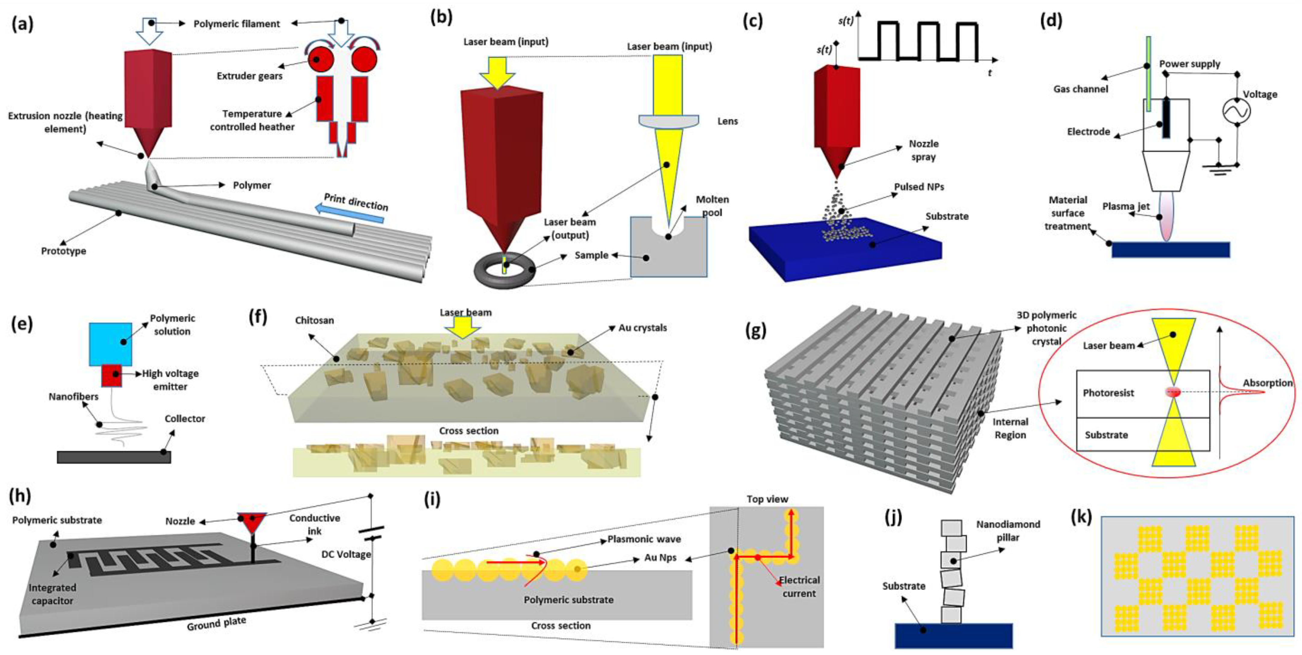
Figure 4.
(a) Poor wetting condition. (b) Good wetting condition (rough surface) controlled by means of a circuit. The surface morphology could be controlled intelligently by a circuit varying, for example, the laser parameters generating surface roughness and, consequently, improving the surface wettability. The figure highlights the possibility to control the wettability by acting on the laser pulse. An example of laser pulse control is discussed in Section 9.
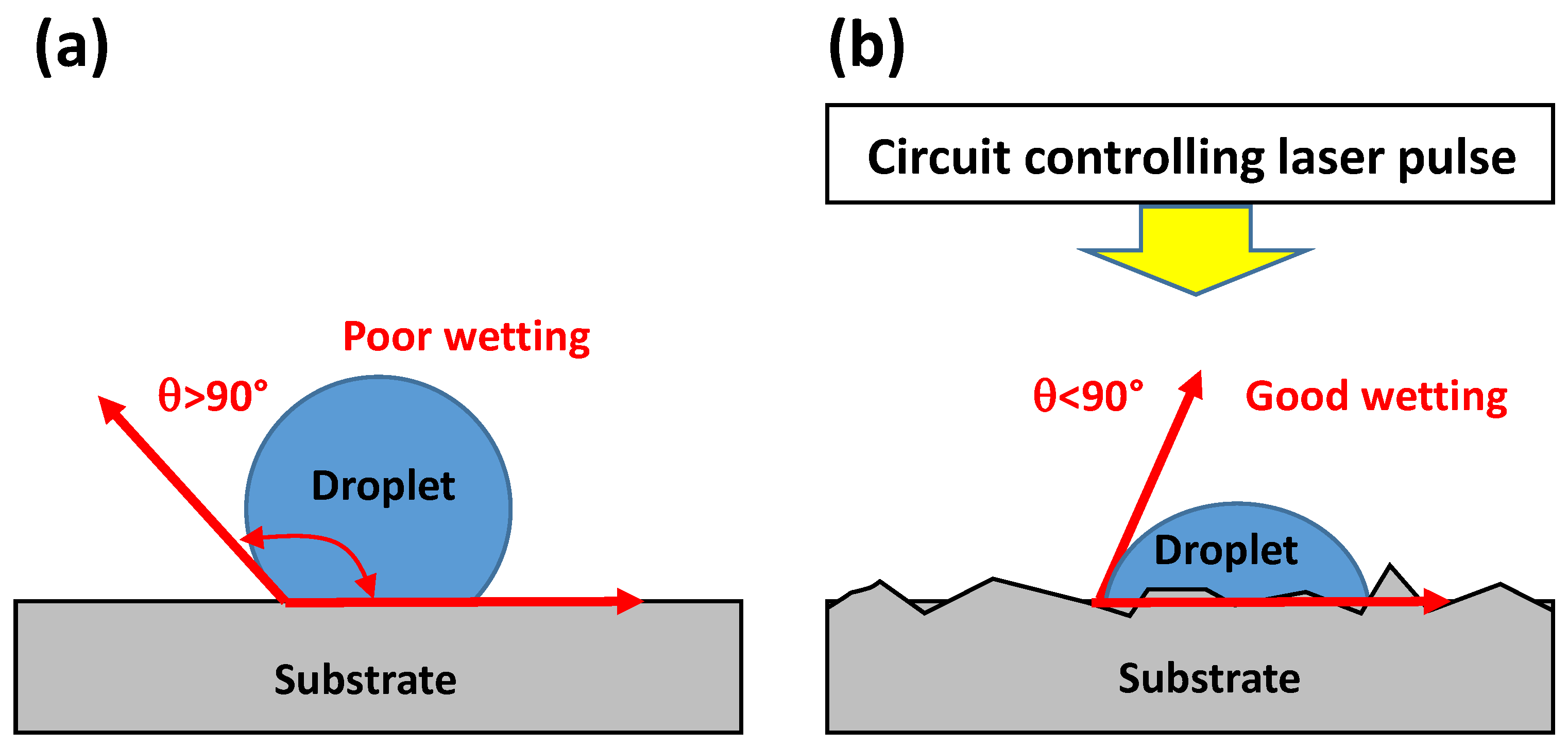
Figure 5.
(a) Sketch of a nanocomposite sample formed by PDMS and GNPs and chemical procedure realizing the PDMS–Au material. (b) Example of shape memory dynamics of a material reacting to stimuli to reconfigure the initial shape after deformation (the control of the external stimuli could be performed by a driven electronic chip). (c) Example of material self-healing regenerating process of a surface crack. (d) Examples of NP typologies: metallic NP, polymeric NP, NP with an oxide layer as coating (NP encapsulated into an oxide coating), NP having a bio-functionalized surface, magnetic NP (torque τ of the magnetic moment m due to the application of an external magnetic field H). (e) NPs moving into a fluid from the channel surface to the middle region (NPs’ velocity profile). (f) Sketch of a nanocomposite electrospun polymeric fiber-based material (Au NP inclusion). The figure summarizes the main steps to realize a nanocomposite materials with GNPs, the reshaping and self-healing process, NPs of different materials, and their possible implementations in nanofluidic and nanocomposite fiber-based materials.

Figure 6.
(a,b) Examples of microporous morphologies. (c) Mesoporous NPs and drug delivery action after the application of external stimuli (for example, by electromagnetic waves). (d) Nanocomposite material for food packaging integrating NPs. Electronics and AI could be applied to optimize the micro–nano devices and food packaging materials. The figure summarizes possible 3D structures and implementations for drug and delivery and food packaging applications.

Figure 7.
(a,b) A 3D model of a graphene layer. (c) Capacitor circuital elements integrated on a flexible substrate (compressed by a pressure force). (d) Inductor circuital elements integrated on a flexible substrate (compressed by a pressure force). (e) Optical device for optical quantum computing. (f) Magnetorheological fluid (NPs aligned to a carrier fluid due to the application of an external magnetic field H). (g) Magnetic NPs flowing into a micro-channel and NP deflection due to the application of a magnetic field. The figure shows the flexible property of graphene and of basic electronic components created on flexible substrates, optical quantum circuit layouts, and magnetic control in nanofluidics.
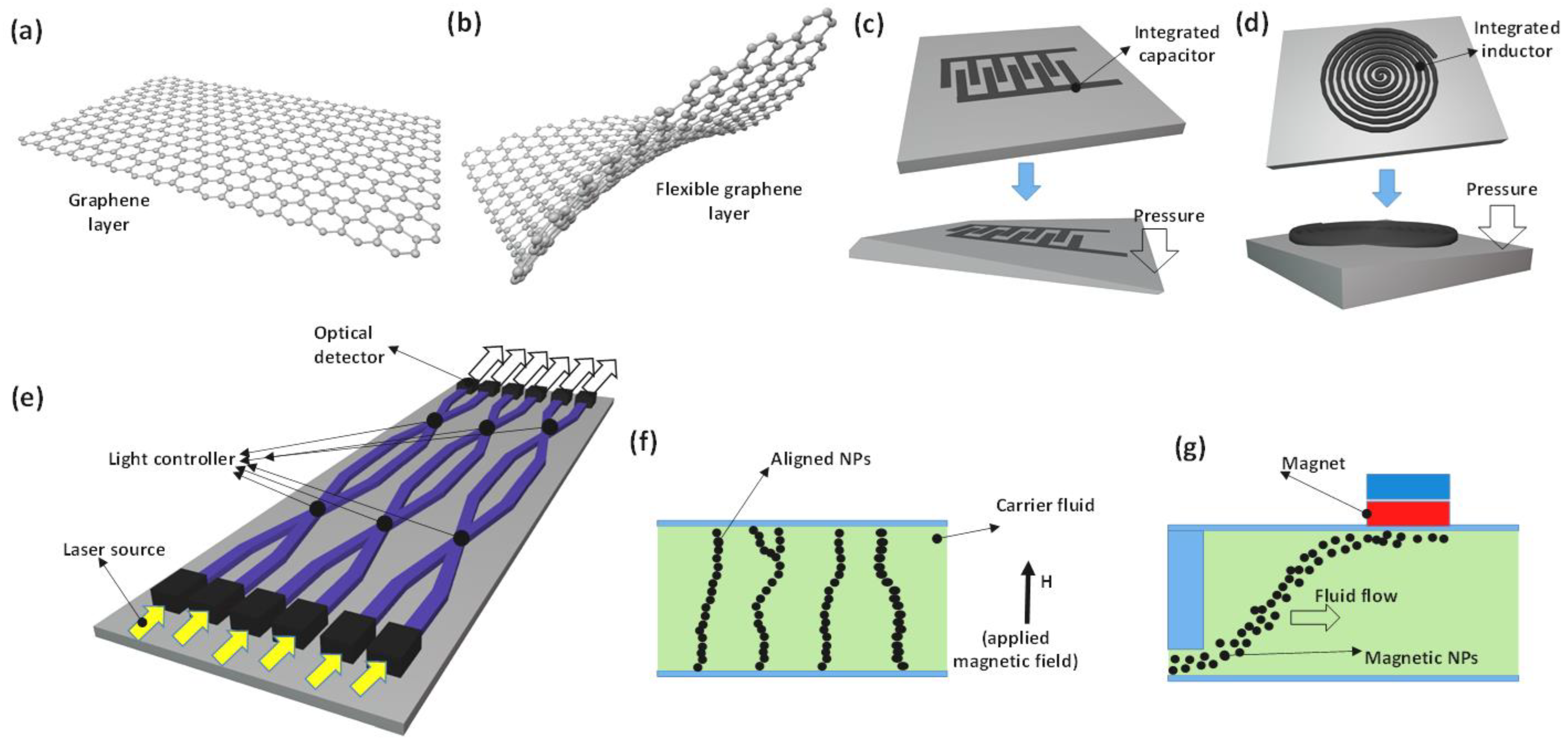
Figure 8.
(a) AI framework to synthetize and improve intelligent materials. (b) Active intelligent process: sketch of the concept of material reconfiguration/regeneration dynamic process by means of AI control. The self-adaptive behavior of the material is to be considered in the small local scale and in the macroscopic scale according to the dimensions of the device. (c) Example of AI control of diode switching signal for machine pulse generation. (d) Concept of potentiometer controlled by AI. (e) Example of an embedded system: schematic block modeling electronic systems with AI controlling stimuli source position and spatial handling. The figure illustrates the role of AI engines in a possible framework suggested by the topics discussed in the review, suitable for material synthesis and control. As further advances in the research field, possible electronic configurations focused on AI circuit control systems regarding the “self-adaptive” behavior of intelligent nanomaterials are suggested.
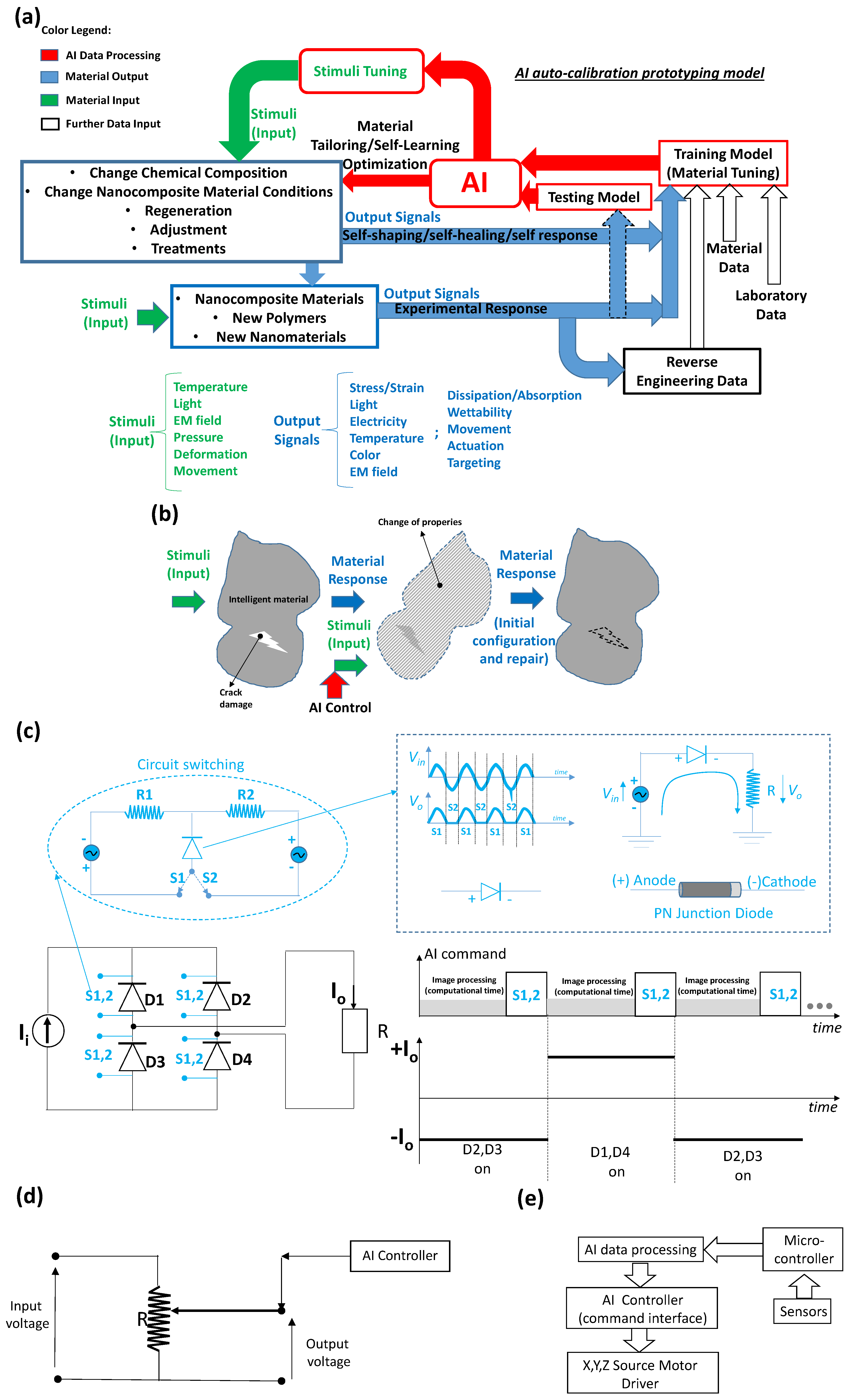
Table 6.
State of the art: materials oriented towards security and connectivity and possible future implementations.
Table 6.
State of the art: materials oriented towards security and connectivity and possible future implementations.
| Macro-Topic (Defined in Step 3) | Application (Step 2) | Description of Application Field (Step 4) | Ref. | Possible Implementation as Intelligent Materials (New Research Topic: Step 5) |
|---|---|---|---|---|
| IoT smart materials | IoT and smart materials in industry | Impact of smart materials in Industry 4.0 scenario [233,234]; sensor prototypes in optoelectronics [235]; smart materials in automotive [236] and aerospace industries [237] | [233,234,235,236,237] | AI controlling production processes of new smart materials adaptable to different application fields |
| Product tags | Functionalized papers behaving as interactive electronic tags for IoT security systems [238]; nanomaterials tagging aquaculture products and monitoring aquatic food processing [239] | [238,239] | AI processing data, ensuring product quality (improvement of quality process) | |
| Health security | Risk detection of chemical and biological agents | Innovative materials and nanosensors detecting chemical/biological threats | [240,241,242,243] | AI defining environmental and biological conditions, ensuring threat detection |
| Food security | Nanotechnology and nanomaterials applied to the whole food supply chain (from agriculture stage to production output) | [244,245,246,247,248] | Algorithms finding possible nano-additives, ensuring food security | |
| Wearable healthcare | Smart materials and wearable systems (facial mask and sensors) | [249,250] | Soft and flexible electronics with AI design and implementation techniques | |
| Alarm and security systems | Future intelligent alarm systems | Quantum computing and hybrid integration (nanomaterials with semiconductor technology) | [251] | AI-based algorithms analyzing compatibility of new nanomaterials with semiconductor technology |
| Miniaturized devices | Miniaturized image vision technology for security systems [252,253,254]; memory chips used in cases of detection of intrusions [255] | [252,253,254,255] | AI data processing to gain information and features extracted from the miniaturized camera by simultaneously processing other data (data fusion including thermal images, ultrasound, etc.) | |
| Intelligent metasurfaces | Metasurfaces controlling information to improve backscattering in wireless communication systems | [256,257] | AI controlling light manipulation and information dispersion | |
| Hybrid composites for civil and military applications | Shape memory alloys (SMA) improving impact damage tolerance | [258] | Systems designed to check the initial shape reconfiguration to automate material restoration | |
| Nanomaterials and nanotechnologies for anti-counterfeiting | Anti-counterfeiting techniques based on light signal processing, micro–nano printing, and laser texturing | [259,260,261,262,263,264,265,266,267,268] |
|
Table 7.
Advantages, limitations, and perspectives of the topics proposed in this work matching with electronics.
Table 7.
Advantages, limitations, and perspectives of the topics proposed in this work matching with electronics.
| Topic | Advantages | Limitations | Perspectives |
|---|---|---|---|
| New materials for electronics | Possibility to adapt circuits to different environments (flexible polymeric substrates); optimization of electrically conductive properties and circuit sensitivity (adding conductive NPs or other nanostructures); possibility to print electrical micro-/nanopatterns on flexible substrates (by conductive ink); NPs as nanoprobes (nanosensors having high sensitivity); new biodegradable materials | Time required to study and test materials for an industrially repeatable production process; time required to check material for quality and use/exposure degradation | Introducing a new concept of electronic substrates partially replacing the semiconductor substrates; new self-reconfigurable materials for robotics applications; new concept of integrated biosensors; single metallic NPs as basic elements to construct nanocircuits; chip controlling biodegradability and deterioration of the material on exposure |
| AI-based tools driving circuits | Implementation of new standalone mechatronic systems optimizing sensing and actuation | Possible AI computational error generating incorrect sensing and actuation | Nanomachines driven by AI-controlled source; new processes monitoring industrial machines or other civil and military environments (alarm systems); new IoT standalone embedded systems |
| AI-based tools for circuit design | AI predicting defects and possible crack risk; AI defining circuit tolerance by processing experimental results; AI reverse engineering and accelerating circuit production process | Unknown AI-based reverse engineering processes to be adapted in the new Industry 5.0 scenario | New concept for the design of innovative circuits in the future scenario of Industry 5.0 |
| New electronic components | Possibility to manufacture miniaturized components in nanoscale adopting nanotechnology; scaling of the electronic technology from micro–nanoscale to millimeter–centimeter scale; realization of new optoelectronic components suitable for quantum computing | Realization of high-tech machines suitable for industrial production (passage from research machine to industrial ones); different computational/processing times of electric signals and optical ones (signal controlling optical quantum chip) | New miniaturized components integrated in intelligent embedded systems; new concept of sensors embedded in intelligent systems; new components for optical quantum computing; new nanocomputing elements; realization of new logic ports implementing AI circuits (McCulloch–Pitts neurons) and simplifying the circuital complexity of the whole embedded system; intelligent chips controlling food quality |
Disclaimer/Publisher’s Note: The statements, opinions and data contained in all publications are solely those of the individual author(s) and contributor(s) and not of MDPI and/or the editor(s). MDPI and/or the editor(s) disclaim responsibility for any injury to people or property resulting from any ideas, methods, instructions or products referred to in the content. |
© 2023 by the author. Licensee MDPI, Basel, Switzerland. This article is an open access article distributed under the terms and conditions of the Creative Commons Attribution (CC BY) license (https://creativecommons.org/licenses/by/4.0/).
Share and Cite
MDPI and ACS Style
Massaro, A. Intelligent Materials and Nanomaterials Improving Physical Properties and Control Oriented on Electronic Implementations. Electronics 2023, 12, 3772. https://doi.org/10.3390/electronics12183772
AMA Style
Massaro A. Intelligent Materials and Nanomaterials Improving Physical Properties and Control Oriented on Electronic Implementations. Electronics. 2023; 12(18):3772. https://doi.org/10.3390/electronics12183772
Chicago/Turabian StyleMassaro, Alessandro. 2023. "Intelligent Materials and Nanomaterials Improving Physical Properties and Control Oriented on Electronic Implementations" Electronics 12, no. 18: 3772. https://doi.org/10.3390/electronics12183772
Note that from the first issue of 2016, this journal uses article numbers instead of page numbers. See further details here.