Communication

W-Band GaN HEMT Switch Using the State-Dependent Concurrent Matching Method

School of Electric Engineering, Soongsil University, 369, Sangdo-ro, Dongjak-gu, Seoul 06978, Republic of Korea
*
Author to whom correspondence should be addressed.
Electronics 2023, 12(10), 2236; https://doi.org/10.3390/electronics12102236
Submission received: 8 April 2023 / Revised: 6 May 2023 / Accepted: 10 May 2023 / Published: 15 May 2023
(This article belongs to the Special Issue Advanced RF, Microwave, and Millimeter-Wave Circuits and Systems)

Abstract

:
In this study, a W-band GaN single-pole single-throw (SPST) switch was designed. To realize the pass and isolation modes of the SPST switch, we proposed the design technique of a unit branch consisting of one transistor and one transmission. The characteristic impedance and length of the transmission line were determined by the impedance and the angle at which the straight line connecting the impedances of the on and off states of the transistor meets the real axis of the Smith chart. Using the design technique, the matching networks for the pass and isolation modes of the switch are concurrently completed. In order to improve the insertion loss and isolation characteristics of the switch, the size of the transistor and the number of unit branches were investigated. To verify the feasibility of the proposed design technique, we designed the W-band SPST switch using a 100 nm GaN HEMT process. The measured insertion loss and isolation were below 2.9 dB and above 23.5 dB, respectively, in the frequency range from 91 GHz to 101 GHz.

1. Introduction

With the innovative development of military science and technology, research on explorers and trackers for the efficient operation of precision launch and hitting systems is being actively conducted. In particular, millimeter wave searchers and tracers are designed mainly using a 96 GHz frequency with low atmospheric loss and a short wavelength. Accordingly, it is essential to develop it as a millimeter-wave monolithic integrated circuit (MMIC) to ensure compact size and excellent performance.
MMICs for such explorers and trackers include power amplifiers, low-noise amplifiers, and switches. In particular, the switch affects the output power of the transmitter and the noise figure of the receiver. The switches require high isolation and high power handling capability and low insertion loss. Switches using p-i-n diodes capable of ensuring good isolation characteristics even at high frequencies have been reported [1,2,3]. However, p-i-n diode switches are not suitable for military millimeter wave searcher and tracking devices where high power is essential because the p-i-n diodes are incompatible with microwave integrated circuits [4]. Therefore, when a p-i-n diode is used, a switch cannot be integrated with other circuits such as power amplifiers and low-noise amplifiers. In this case, additional power loss and bandwidth reduction may occur during the modularization process of connecting the transceiver circuits and the switch [5]. This problem becomes more serious in the W-band with a high operating frequency. Therefore, research on switches using high electron-mobility transistor (HEMT) devices compatible with MMIC is being actively conducted [4,6,7,8,9,10,11,12,13]. In particular, gallium nitride (GaN) HEMT has a faster switching speed and high band gap characteristics compared to silicon-, gallium arsenide (GaAs)-, and silicon germanium (SiGe)-based devices. Accordingly, GaN HEMT can handle high power at a high operating frequency such as a W-band [14]. As a result, GaN HEMT can be regarded as one of the promising candidate devices among the MMICs for explorers and trackers. In this work, we conducted a study on a single-pole single-throw (SPST) switch using GaN HEMT.
In this study, we proposed a design methodology that can achieve simultaneous matching for on and off states of traveling-wave-type SPST switches using the GaN HEMT process. The design methodology utilizes the parasitic components of GaN HEMT and additional transmission lines. Many studies related to the design methodologies for traveling-wave type switches have already been introduced [15,16]. However, most of the previous works are based on mathematical methodology. In this study, for the design of the traveling-wave type switch, we proposed a technique to design the characteristic impedance and length of the transmission line from impedances at on and off states of transistors using the Smith chart.

2. Proposed Design Technique of the W-Band Switch

The design process of the proposed methodology can be summarized as follows. The key components of the proposed switch are transistors and transmission lines. At this time, the transmission line is connected in series with the drain of the transistor. First, impedances according to the on and off states of the transistor are checked on the Smith chart. Thereafter, the impedance of each state is connected in a straight line on the Smith chart. The point where the straight line connecting the two impedances meets the real axis of the Smith chart is referred to as the characteristic impedance of the transmission line. In addition, the length of the transmission line is determined by the angle between this straight line and the real axis. In this way, impedance matching for the on and off state of the traveling-wave-type SPST switch may be achieved simultaneously. The following describes the actual design process of the proposed design methodology.
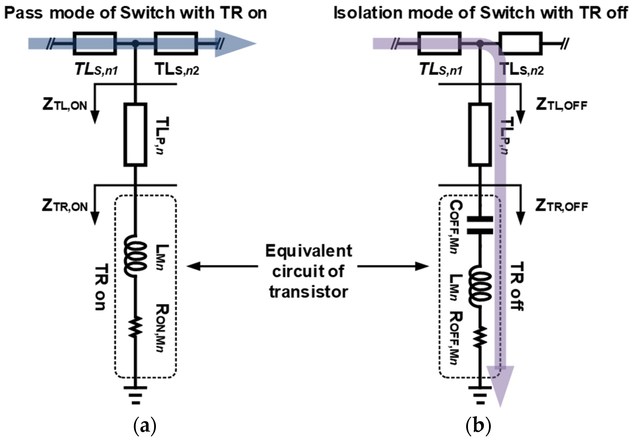
The designed switch consists of a unit branch as shown in Figure 1. The transmission line of TLS connects the port of the RFIN and the port of the RFOUT. For 50 Ω load impedance, the transmission line of TLS was designed to have a characteristic impedance of 50 Ω. In the final optimization process of the switch, the length of the TLS was adjusted to improve the input and output return losses. In Figure 2, the equivalent circuit of the unit branch is shown. In the case of the unit branch, it is composed of an HEMT transistor and a transmission line of TLP. The transmission line of TLP connects the drain of the transistor and the transmission line of TLS. The transistor and TLP determine the pass and isolation mode characteristics of the entire traveling-wave-type SPST switch.
As illustrated in Figure 2, ZTR,ON and ZTR,OFF are impedances due to the parasitic components of the transistor depending on the on and off states of the transistor, respectively. In Figure 2, for the convenience of analysis, it is assumed that the ground connected to the source of the transistor is ideal. When the transistor is on, the transistor is equivalent to the inductance (LM) and the resistance (RON). On the other hand, when the transistor is off, the transistor is equivalent to inductance (LM), capacitance (COFF), and resistance (ROFF) [4,14,17,18]. Here, the transistor in the off state may be modeled in parallel with the resistance and the capacitance. However, in this study, the transistor in the off state was modeled with a series circuit of resistance and capacitance through parallel-to-series conversion.
Figure 3 shows the tendency of impedance change according to the on and off state of the transistor. In Figure 3, the values of ZTR,ON and ZTR,OFF are not actual values but are values for conceptualizing the proposed design technique. When points ZTR,ON and ZTR,OFF on the Smith chart were connected in a straight line, the impedance of the point where the straight line and the real axis of the Smith chart meet was set as the characteristic impedance value of the TLP. Thereafter, the impedances of ZTR,ON and ZTR,OFF were moved on the real axis using the θ value adjusted according to the length of the TLP.
If l is the length of the TLP, the equations for determining the characteristic impedance, Z0, and θ of TLP are as follows:
Z T R , O N = a + j b , Z T R , O F F = c + j d , β = θ l
Z T L , O N = Z 0 a + j b + Z 0 tan β l Z 0 + j a + j b tan β l , Z T L , O F F = Z 0 c + j d + Z 0 tan β l Z 0 + j c + j d tan β l
Z 0 2 tan β l + b 1 tan 2 β l Z 0 a 2 + b 2 tan β l = 0 Z 0 2 tan β l + d 1 tan 2 β l Z 0 c 2 + d 2 tan β l = 0
Z 0 2 = d a 2 + b 2 b c 2 + d 2 d b for tan β l > > 1 , tan β l < < 1 a 2 + b 2 = c 2 + d 2 for tan β l 1
tan β l = Z 0 b 1 a 2 + b 2 d b d a 2 + b 2 b c 2 + d 2 for tan β l > > 1 1 for tan β l 1 d b a 2 + b 2 c 2 + d 2 Z 0 for tan β l < < 1
The ZTR,ON and ZTR,OFF moved by the TLP are shown in Figure 3 as ZTL,ON and ZTL,OFF, respectively. From the perspective of the whole SPST switch, ZTL,ON has a relatively high resistance and ZTL,OFF has a relatively low resistance, so the on and off states of the transistor were used as the pass and isolation modes of the switch, respectively, as shown in Figure 3. Consequently, the proposed design technique of the switch could realize the pass and isolation modes of the switch by adjusting the characteristic impedance and length of the transmission line, TLP according to the on and off impedances of the transistor.

3. Design of the W-Band SPST Switch

A W-band SPST switch based on the 100 nm GaN HEMT process was designed using the proposed design methodology for the switch. First, we investigated the transistor size of the unit branch to obtain low insertion loss and high isolation performance in the pass and isolation modes of the SPST switch as shown in Figure 4.
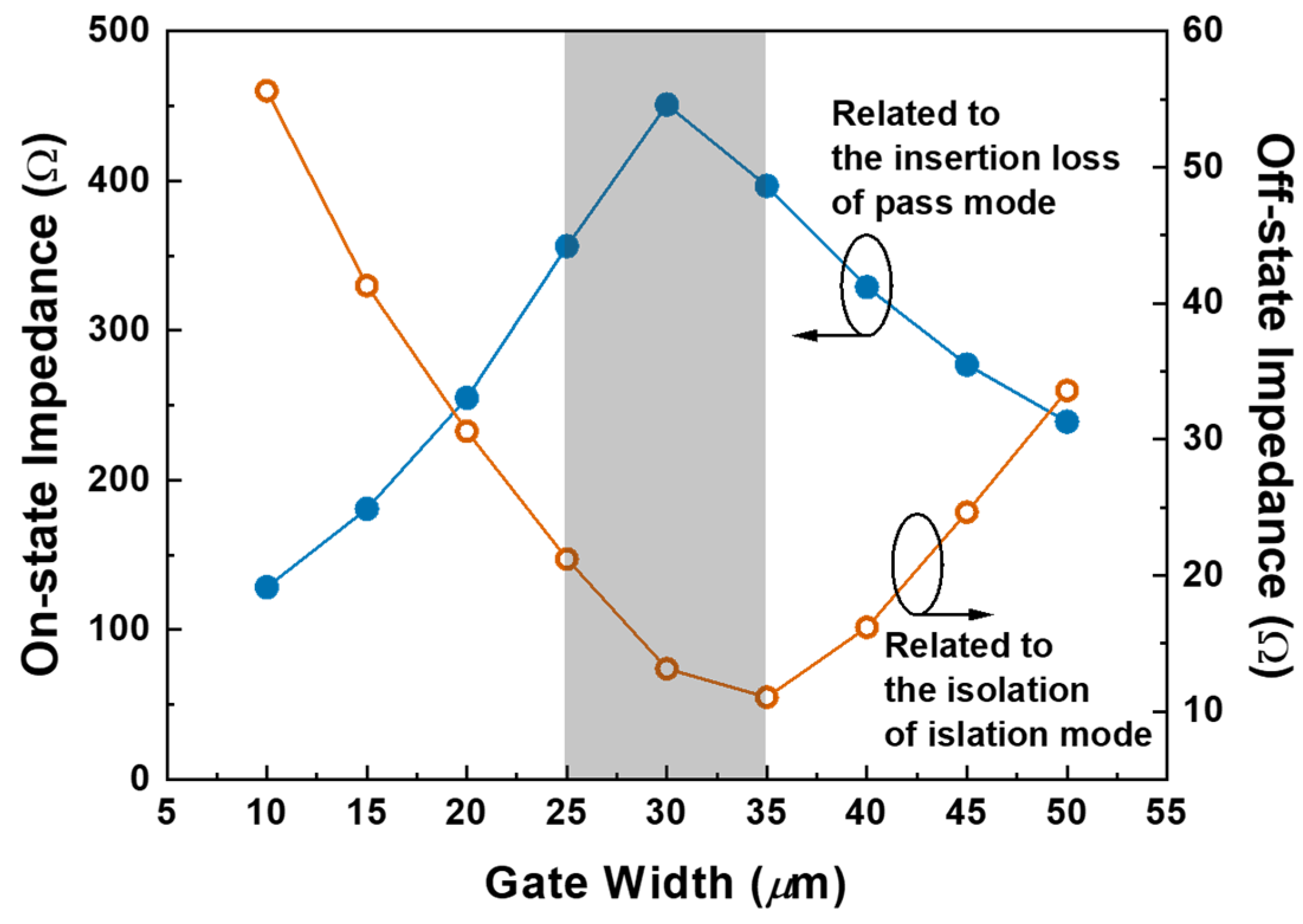
As previously described, the proposed switch operates in pass mode when the transistor is off. Conversely, the switch operates in isolation mode when the transistor is on. Therefore, it is advantageous for the individual transistors that make up the switch to have high and low impedances in the on and off states, respectively. Figure 4 shows the impedance of the transistor according to the gate width of the transistor when the transistor is in the on and off states. As shown in Figure 4, the insertion loss and isolation characteristics can be improved when the gate width is from 25 μm to 35 μm. In this study, 30 μm was used as the initial value of the gate width, while the gate length and operating frequency were 100 nm and 96 GHz, respectively.
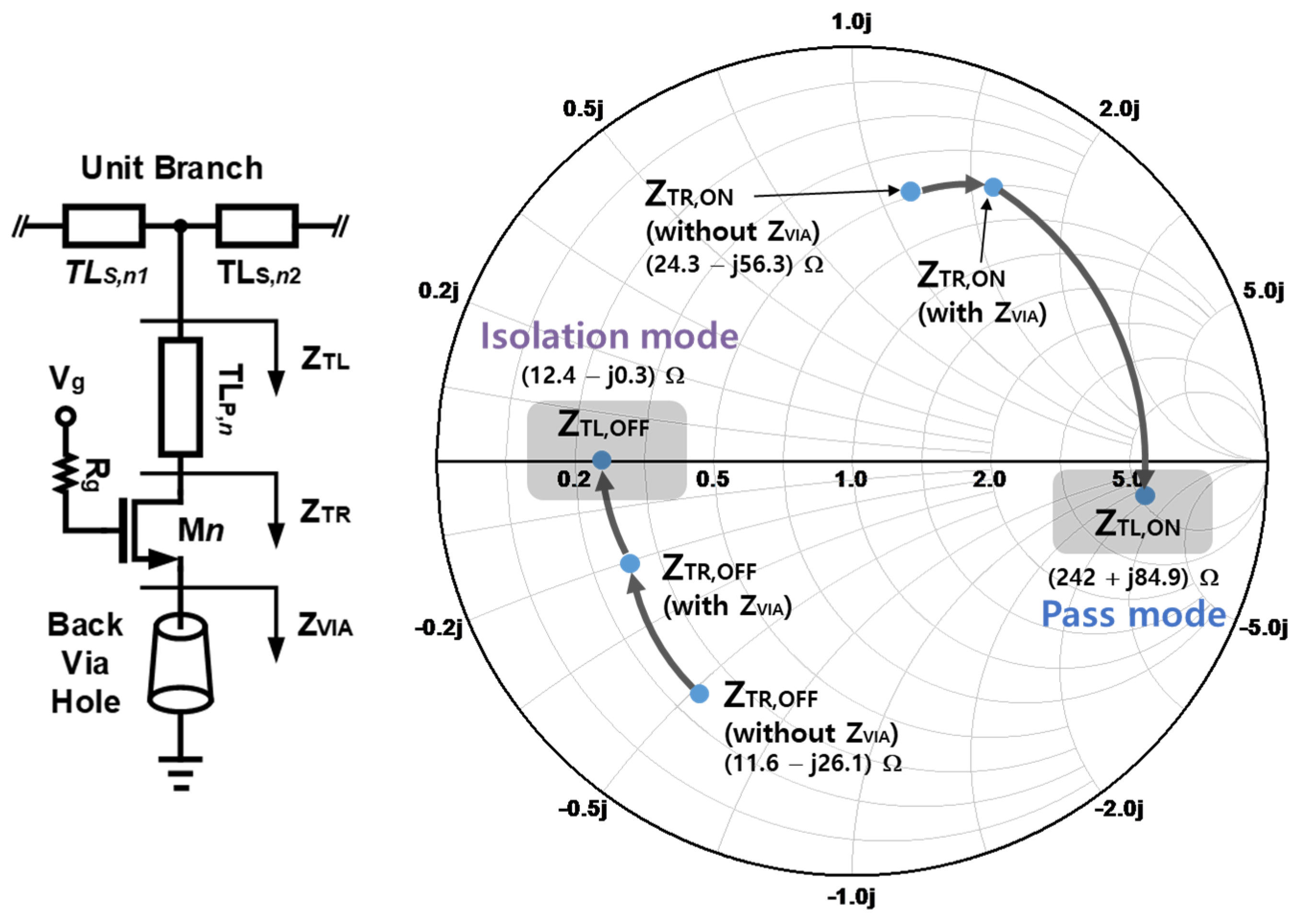
The unit branch with a transistor of 30 μm gate length was designed, as illustrated in Figure 5, using the proposed design methodology. The source of the transistor is connected to the ground through the back via a hole. Here, the effect of the back via the hole provided for ground in the GaN HEMT process was considered. The on and off states of the transistor are controlled by the gate voltage, and the gate is connected to the voltage source through Rg of 5 kΩ. In Figure 5, the impedance trajectory at the unit branch is shown using the Smith chart. The actual design process shown in Figure 5 is very similar to the conceptual diagram of the proposed design methodology shown in Figure 3.
As the next step, the number of unit branches constituting the SPST switch was determined through the insertion loss and isolation characteristics. As shown in Figure 6, as the number of unit branches increases, the isolation characteristic improves, but the insertion loss degrades, so we chose the number of unit branches to be three.
As a result, the schematic of the designed SPST switch is configured as shown in Figure 1. However, the size of the transistor slightly changed during the final detailed tuning process. Finally, the used gate widths of M1, M2, and M3 were 25 μm, 30 μm, and 25 μm, respectively.

4. Measurement Results

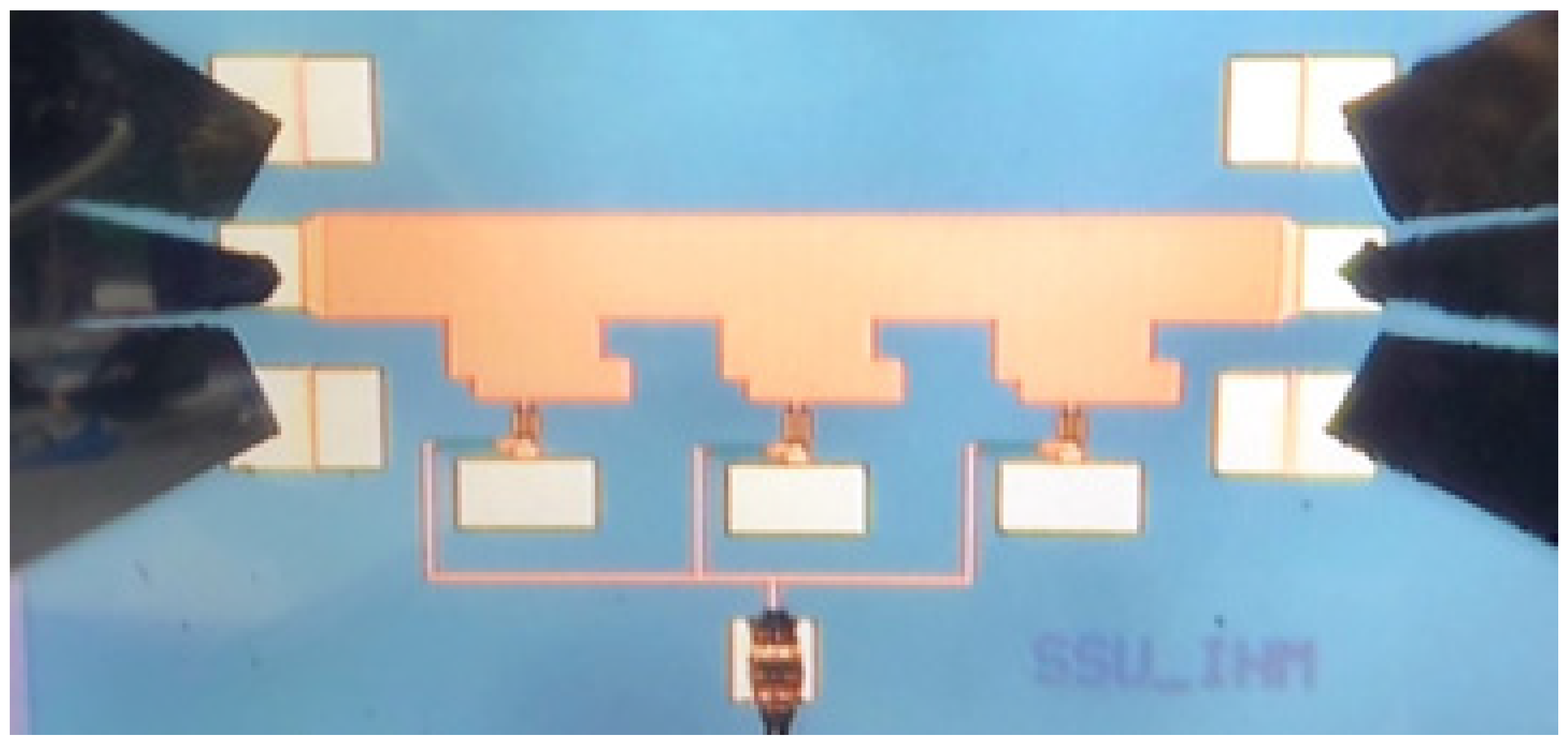
We designed a W-band SPST switch using a 100 nm GaN HEMT process to verify the feasibility of the proposed design technique. Figure 7 shows the chip photograph of the designed SPST switch with a chip size of 1.13 × 0.67 mm2 including test pads. For measurement, Rohde & Schwarz’s ZVA67 network analyzer and ZVA-Z110E converter were used. For the measurement of power handling capability, a driver amplifier and an attenuator were used. The gate voltages for the isolation and pass modes were −1.4 V and 0 V, respectively.
Figure 8 shows the measured insertion loss and isolation characteristics. The measurement results showed a similar tendency to the simulation as a whole, although the insertion loss was somewhat degraded compared to the simulation results. Insertion loss and isolation were measured below 2.9 dB and above 23.5 dB, respectively, in the range of operating frequencies from 91 GHz to 101 GHz.
As shown by the measured S-parameters of Figure 9, both S11 and S22 were measured to be −10 dB or less in the measurement frequency range of 75 GHz to 105 GHz.
Figure 10 shows the measured output power according to the input power in the operating frequency of 96 GHz. In general, when the switch operates in pass mode while the transistor constituting the switch is off, the power handling capability is limited by the breakdown voltages between the drain-source or drain-gate of the transistors. On the other hand, in this study, it is advantageous in terms of power handling capability because the switch operates in pass mode while the transistors constituting the switch are on. At the 96 GHz operating frequency, the output power of the switch has a loss of 2.68 dB compared to the input power. As shown in Figure 10, 0.23 dB compression was measured at an output power point of 12.4 dBm with 14.9 dBm input power. The higher output power could not be measured due to the power limit of the equipment we used. Therefore, the input P1dB and output P1dB of the designed switch may be higher than 14.9 dBm and 12.4 dBm, respectively.
Table 1 summarizes the performance of state-of-the-art switches. As shown in Table 1, the designed switch has a somewhat narrow operating frequency range, but has reasonable insertion loss and isolation, and the input P1dB of the switch also exceeds 14.9 dBm. In addition, if the gate length of the GaN HEMT used in the switch decreases, the on-resistance decreases. Therefore, when using GaN HEMT with a reduced gate length, insertion loss is expected to be improved in the pass mode of the switch.

5. Conclusions

In this study, for the design of a W-band SPST switch, a design technique for determining the characteristic impedance and length of a transmission line after confirming the impedance of the transistor has been proposed. The proposed design methodology consists of one transistor and one transmission line. At this time, the transmission line is connected in series with the drain of the transistor. The characteristic impedance and length of the transmission line were determined by the impedance and the angle at which the straight line connecting the impedances of the on and off states of the transistor meets the real axis of the Smith chart. Accordingly, the impedance matching networks of the on and off states of the traveling-wave-type SPST switch were simultaneously completed. In addition, in order to improve the pass and isolation mode characteristics of the switch, the transistor size was investigated, and the number of unit branches was optimized. As a result, the switch was designed with a total of three unit branches using the proposed design technique. The measured insertion loss and isolation were below 2.9 dB and above 23.5 dB, respectively, in the frequency range from 91 GHz to 101 GHz. The measured output P1dB was higher than 12.4 dBm in the operating frequency of 96 GHz.

Author Contributions

Conceptualization, H.I. and C.P.; methodology, H.I., J.L. and C.P.; investigation, H.I.; supervision, C.P.; writing—original draft, H.I. and J.L.; review and editing C.P. All authors have read and agreed to the published version of the manuscript.

Funding

This work was supported in part by a National Research Foundation of Korea (NRF) grant funded by the Korean government (MSIT) (No. 2021R1A2C1013666) and in part by the Development of Civil Military Technology Project (No. 21-CM-RA-02) from the Institute of the Civil Military Technology Cooperation (ICMTC).

Data Availability Statement

All the data included in the study are mentioned in the article.

Conflicts of Interest

The authors declare no conflict of interest.

References

  1. Lam, K.; Ding, H.; Liu, X.; Orner, B.A.; Rascoe, J.; Bewitt, B.; Mina, E.; Gaucher, B. Wideband millimeter wave pin diode SPDT switch using IBM 0.13 μm SiGe technology. In Proceedings of the 2007 IEEE European Microwave Integrated Circuit Conference, Munich, Germany, 8–10 October 2007; pp. 108–111. [Google Scholar]
  2. Hongtao, W.; Xuebang, G.; Hongjang, W.; Bihua, W.; Yanan, L. W-band GaAs pin diode SPST switch MMIC. In Proceedings of the 2012 IEEE International Conference on Computational Problem-Solving (ICCP), Leshan, China, 19–21 October 2012; pp. 93–95. [Google Scholar]
  3. Song, P.; Schmid, R.L.; Ulusoy, A.C.; Cressler, J.D. A highpower, low-loss W-band SPDT switch using SiGe PIN diodes. In Proceedings of the 2014 IEEE Radio Frequency Integrated Circuits Symposiu, Tampa, FL, USA, 1–3 June 2014; pp. 195–198. [Google Scholar]
  4. Lin, K.-Y.; Tu, W.-H.; Chen, P.-Y.; Chang, H.-Y.; Wang, H.; Wu, R.-B. Millimeter-wave MMIC passive HEMT switches using traveling-wave concept. IEEE Trans. Microw. Theory Tech. 2004, 52, 1798–1808. [Google Scholar] [CrossRef]
  5. Monayakul, S.; Sinha, S.; Weimann, N.; Schmückle, F.J.; Hrobak, M.; Krozer, V.; John, W.; Weixelbaum, L.; Wolter, P.; Krüger, O.; et al. Flip-Chip Interconnects for 250 GHz Modules. IEEE Microw. Wirel. Compon. Lett. 2015, 25, 358–360. [Google Scholar] [CrossRef]
  6. Lin, K.Y.; Wang, Y.J.; Niu, D.C.; Wang, H. Millimeter-wave MMIC single-pole-double throw passive HEMT switches using impedance-transformation networks. IEEE Trans. Microw. Theory Tech. 2003, 51, 1076–1085. [Google Scholar] [CrossRef]
  7. Thome, F.; Ture, E.; Bruckner, P.; Quay, R.; Ambacher, O. W-Band SPDT Switches in Planar and Tri-Gate 100-nm Gate-Length GaN-HEMT Technology. In Proceedings of the 2018 11th IEEE German Microwave Conference (GeMiC), Freiburg, Germany, 12–14 March 2018; pp. 331–334. [Google Scholar]
  8. Thome, F.; Ambacher, O. Highly-Isolating and Broadband Single-Pole Double-Throw Switches for Millimeter-Wave Applications up to 330 GHz. IEEE Trans. Microw. Theory Tech. 2018, 66, 1998–2009. [Google Scholar] [CrossRef]
  9. Thome, F.; Massler, H.; Wagner, S.; Leuthe, A.; Kallfass, I.; Schlechtweg, M.; Ambacher, O. Comparison of two W-band low-noise amplifier MMICs with ultra low power consumption based on 50 nm InGaAs mHEMT technology. In Proceedings of the 2013 IEEE MTT-S International Microwave Symposium Digest (MTT), Seattle, WA, USA, 2–7 June 2013; pp. 1–4. [Google Scholar]
  10. Dyskin, A.; Peleg, N.; Wagner, S.; Ritter, D.; Kallfass, I. An asymmetrical 60–90 GHz single-pole double throw switch MMIC. In Proceedings of the 2013 IEEE European Microwave Integrated Circuit Conference, Nuremberg, Germany, 6–8 October 2013; pp. 145–148. [Google Scholar]
  11. Tsai, Z.-M.; Yeh, M.-C.; Lei, M.-F.; Chang, H.-Y.; Lin, C.-S.; Wang, H. DC-to-135 GHz and 15-to-135 GHz SPDT traveling wave switches using FET-integrated CPW line structure. In Proceedings of the IEEE MTT-S International Microwave Symposium Digest, Long Beach, CA, USA, 17 June 2005; pp. 1–4. [Google Scholar]
  12. Kallfass, I.; Diebold, S.; Massler, H.; Koch, S.; Seelmann-Eggebert, M.; Leuther, A. Multiple-throw millimeter-wave FET switches for frequencies from 60 up to 120 GHz. In Proceedings of the 2008 38th IEEE European Microwave Conference, Amsterdam, The Netherlands, 27–31 October 2008; pp. 1453–1456. [Google Scholar]
  13. Kim, J.; Ko, W.; Kim, S.-H.; Jeong, J.; Kwon, Y. A high-performance 40–85 GHz MMIC SPDT switch using FET-integrated transmission line structure. IEEE Microw. Wirel. Compon. Lett. 2003, 13, 505–507. [Google Scholar]
  14. Kim, T.; Im, H.; Lee, S.-H.; Kim, K.-J.; Park, C. Highly Linear K-/Ka-Band SPDT Switch Based on Traveling-Wave Concept in a 150-nm GaN pHEMT Process. IEEE Microw. Wirel. Compon. Lett. 2022, 32, 987–990. [Google Scholar] [CrossRef]
  15. Singh, A.; Mandal, M.K. Parasitic Compensation and Hence Isolation Improvement of PIN Diode-Based Switches. IEEE Trans. Circuits Syst. II-Express Briefs 2021, 68, 97–101. [Google Scholar] [CrossRef]
  16. Xu, Z.; Xu, J.; Cui, Y.; Guo, J.; Qian, C. A low-cost W-band SPDT switch with Q-MMIC concept using quartz substrate. J. Electromag. Waves Appl. 2018, 32, 428–438. [Google Scholar] [CrossRef]
  17. Trinh, K.T.; Kao, H.-L.; Chiu, H.-C.; Karmakar, N.C. A Ka-Band GaAs MMIC Traveling-Wave Switch with Absorptive Characteristic. IEEE Microw. Wirel. Compon. Lett. 2019, 29, 394–396. [Google Scholar] [CrossRef]
  18. Zhao, L.; Liang, W.-F.; Zhou, J.-Y.; Jiang, X. Compact 35–70 GHz SPDT Switch with High Isolation for High Power Application. IEEE Microw. Wirel. Compon. Lett. 2017, 27, 485–487. [Google Scholar] [CrossRef]
  19. Margomenos, A.; Kurdoghlian, A.; Micovic, M.; Shinohara, K.; Moyer, H.; Regan, D.C.; Grabar, R.M.; McGuire, C.; Wetzel, M.D.; Chow, D.H. W-Band GaN Receiver Components Utilizing Highly Scaled, Next Generation GaN Device Technology. In Proceedings of the 2014 IEEE Compound Semiconductor Integrated Circuit Symposium (CSICS), La Jolla, CA, USA, 19–22 October 2014; pp. 1–4. [Google Scholar]
  20. Sonnenberg, T.; Romano, A.; Verploegh, S.; Pinto, M.; Popović, Z. V- and W-Band Millimeter-Wave GaN MMICs. IEEE J. Microw. 2023, 3, 453–465. [Google Scholar] [CrossRef]
Figure 1. Schematic of the designed W-band SPST switch.
Electronics 12 02236 g001
Figure 2. Equivalent circuit according to the transistor being on and off: (a) pass and (b) isolation modes of the SPST switch.
Electronics 12 02236 g002
Figure 3. Impedances according to the on and off state of the transistors and the impedance changes due to TLP.
Electronics 12 02236 g003
Figure 4. Impedance of the transistor according to the gate width with the gate length of 100 nm and the operating frequency of 96 GHz.
Electronics 12 02236 g004
Figure 5. Unit branch design: impedance matching process.
Electronics 12 02236 g005
Figure 6. Switch characteristics based on the number of unit branches: (a) insertion loss and (b) isolation.
Electronics 12 02236 g006
Figure 7. Chip photograph of the designed switch (chip size: 1.13 × 0.67 mm2).
Electronics 12 02236 g007
Figure 8. Measurement results: insertion loss and isolation.
Electronics 12 02236 g008
Figure 9. Measurement results: S-parameters.
Electronics 12 02236 g009
Figure 10. Measurement results: output power according to the input power.
Electronics 12 02236 g010
Table 1. Performance comparison of state-of-the-art GaN switches.
[19][20][20][20]This Work
StructureSPSTSPSTSPSTSPDTSPST
Tech. (nm)40404040100
Freq. (GHz)60–11075–11075–11075–11091–101
Insertion loss (dB)0.9–1.40.9–3.51.0–2.21.8–8.0<2.9
Isolation (dB)>925–3015–2030–40>23.5
IP1dB (dBm)>24>10 (1)>10 (1)>10 (1)>14.9 (2)
Chip size (mm2)0.544---0.757
(0.306 (3))
(1) Peak large-signal values, (2) limited by available source power, and (3) core size.
Disclaimer/Publisher’s Note: The statements, opinions and data contained in all publications are solely those of the individual author(s) and contributor(s) and not of MDPI and/or the editor(s). MDPI and/or the editor(s) disclaim responsibility for any injury to people or property resulting from any ideas, methods, instructions or products referred to in the content.