Article

A Comparative Analysis of S-S and LCCL-S Compensation for Wireless Power Transfer with a Wide Range Load Variation

1
School of Advanced Technology, Xi’an Jiaotong-Liverpool University, Suzhou 215123, China
2
Department of Electrical Engineering and Electronics, University of Liverpool, Liverpool L69 3GJ, UK
3
Gpower Semiconductor Company, Suzhou 215123, China
*
Author to whom correspondence should be addressed.
Electronics 2022, 11(3), 420; https://doi.org/10.3390/electronics11030420
Submission received: 27 December 2021 / Revised: 23 January 2022 / Accepted: 26 January 2022 / Published: 29 January 2022

Abstract

:
Wireless power transmission (WPT) has great potential for charging electric vehicles. Constant voltage (CV) and constant current (CC) are two major types of battery charging modes. In this paper, we analyze the output characteristics of series-series (S-S) topology and double capacitances and inductances-series (LCCL-S) topology. Voltage gain variation is achieved in the LCCL-S compensation structure without additional components, and the system is still kept in resonant condition. A WPT experimental platform was also built and tested based on the theoretical analysis. When the load resistance is 300 Ω, a voltage gain of 0.7 or 2.22 is achieved for the LCCL-S with a compensating inductor of 100 μH or 33 μH, respectively. The experimental results fit the theoretical analysis. The CC/CV output characteristics and efficiencies of S-S and LCCL-S topologies in a wide load resistance range are also demonstrated. Moreover, zero voltage switch (ZVS) is also implemented in both two systems.

1. Introduction

With the growth of the electric vehicle industry in recent years and the limitations of battery capacity, a flexible, safe, and efficient charging method is required [1]. Compared to traditional plug-in wired charging, wireless power transmission (WPT) eliminates the need for charging cables and plugs. Meanwhile, the potential risk of electric shock is also reduced. Furthermore, the charging device can be designed to be more hermetically sealed, which allows it to be more suitable for extreme operating condition, such as rain, snow, and typhoons [2].
To increase the efficiency and reduce the reactive power of the WPT system, it is necessary to achieve the resonant condition for both transmitter and receiver sides [3]. There are four types of traditional resonant topologies using a capacitor compensated coil on one side as series-series (S-S), Series-Parallel (S-P), Parallel-Series (P-S), Parallel-Parallel (P-P) [4]. Aubakirov [5] from the National Research University of Electronic Technology optimizes the S-S and S-P topology, while the S-P topology is limited by load variations.
These traditional topologies are strongly influenced by the loosely coupled transformer (LCT) parameters [6]. Therefore, researchers proposed higher-order compensation networks to increase the system design freedom such as LCL, LCCL. Yao et al. [6] used the double side-LCL (DS-LCL) topology with conventional compensation and improved compensation with parameter tuning to achieve 200 W output and reduce harmonics in the system. Kavimandan et al. [7] compared the tolerance of LCCL-S with LCCL-P for the case where the coils are aligned. It was found that LCCL-P possesses better resistance to offsets, while the LCCL-S topology is used to reduce the reactive power. Chen et al. [8] investigated the output characteristics of the S-S and LCCL-S topologies under detuned condition. The results demonstrate that the S-S topology has better performance to high power levels condition, while the LCCL-S topology can achieve higher efficiency at lower power levels. Moreover, due to the charging characteristics of Li-ion batteries, the constant voltage (CV) or constant current (CC) output of the topology needs to be addressed [9]. Li et al. [10] proposed a parameter tuning method for the DS-LCC topology. This method can be used to achieve CC output and to realize zero phase angle, which improves the power factor of the system. Chen et al. [11] propose an asymmetric parameter tuning method that varies the values of the two compensating inductors of the LCC-LCC topology. The efficiency of the system is improved without changing the system CC output. However, too many passive components will cause extra loss [12]. Li et al. [13] also demonstrated that the S-S topology possesses higher efficiency than the LCL-S topology. In addition, wide band semiconductor devices are used to improve the efficiency of WPT systems due to their excellent performance [14]. Qian et al. verified that cascade GaN HEMTs have efficiency advantages for Si MOS over the wide load range in WPT system [15]. As mentioned by Hu et al. [16] and Vitols et al. [17], the required voltage levels are specified for different loads. Electric vehicles have DC voltages from a few volts to several hundred volts depending on the battery packs, while the electric scooter only requires a low voltage level of 24–72 V. Laha et al. [18] utilized a cascade converter to vary the output voltage at the secondary side by an external control system. However, this method causes additional power losses and raises costs. Thus, to investigate the tuning of topological parameters to produce different voltage gains for the same coil is necessary.
In this paper, the main purpose is to investigate the implementation of the LCCL-S topology with varying voltage gain, without adding additional components and ensuring a resonant state. The equivalent circuit models of two topologies, S-S and LCCL-S, are analyzed. The S-S is utilized for the CC model, and two sets of LCCL-S topologies for the CV model with different voltage gains are designed. A WPT experimental platform was built to demonstrate the output implementation of two optimized LCCL-S topologies and the S-S topology over a wide range of load variations.

2. S-S and LCCL-S WPT System Modeling Analysis

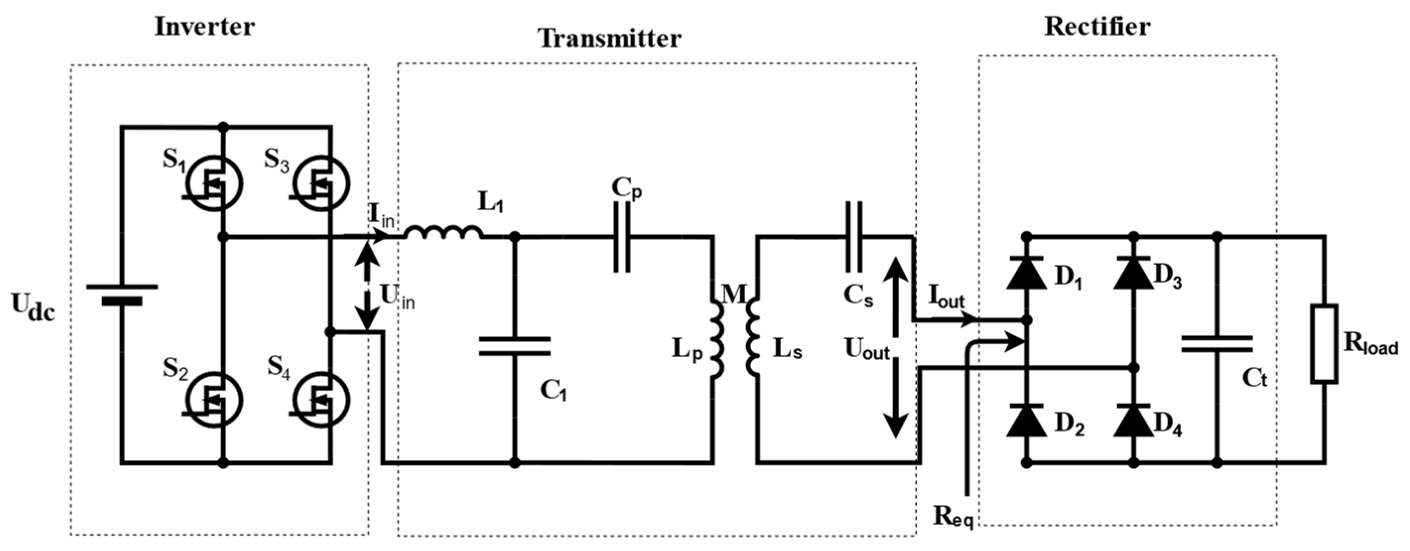
2.1. WPT System Structure

The WPT system diagram used in this paper is shown in Figure 1. It mainly contains four components: full bridge inverter (FBI), transmitter, rectifier circuit, and load resistance. For the transmitter part, there is a transmitting coil and a receiving coil with correspondent resonant compensation circuits. Udc is the DC supply voltage. S1S4 are the four transistors used in the FBI. Uin and Uout are the input and output voltages of the resonant network, respectively. Iin and Iout are the input and output current of the resonant network, respectively. L1 is the inductance in the LCCL-S topology. C1, Cp, and Cs are the capacitances in this topology. Lp and Ls represent the self-inductance of the transmitter-receiver coils. M represents the mutual inductance between the coils. Req is the equivalent load on the secondary side. D1D4 are the four diodes used in the rectifier. Ct is the rectifier filter capacitor. Rload is the load resistor.
On the primary side, the DC source Udc is converted to a square wave voltage Uin through the FBI and then flow into the resonance compensation topology. On the secondary side, a full bridge rectifier filter is utilized for converting the transferred AC voltage into DC voltage to load resistance.
T-type model is widely used to analyze WPT charging systems [19,20]. The model of a T-type circuit is shown in Figure 2. Z1, Z2, and Z3 are the impedance values on each branch of the T-type circuit and ZL-T is the load impedance of the T-type circuit. When Z1 = Z2 = Z3 = jX, the topology achieves conversion from a constant current supply to a constant voltage supply, or from constant voltage input to constant current output [21]. X represents the value of reactance, and the unit imaginary number is represented by j. While achieving these functions, the T-type circuit can also achieve zero phase angle (ZPA) if the load is purely resistive.
The equation for the conversion of a CV source to a CC source is:
I o u t - T = U i n - T j X
U i n - T is the input voltage of the T-type circuit. I o u t - T is the output current of this circuit.
The equation for the conversion of a CC source to a CV source is:
U o u t - T = j X I i n - T
I i n - T is the input current of the T-type circuit. U o u t - T is the output voltage of this circuit.
Input impedance is set to Zin-T. Its input impedance is:
Z i n - T = X 2 Z L - T
ZL-T is the load impedance.

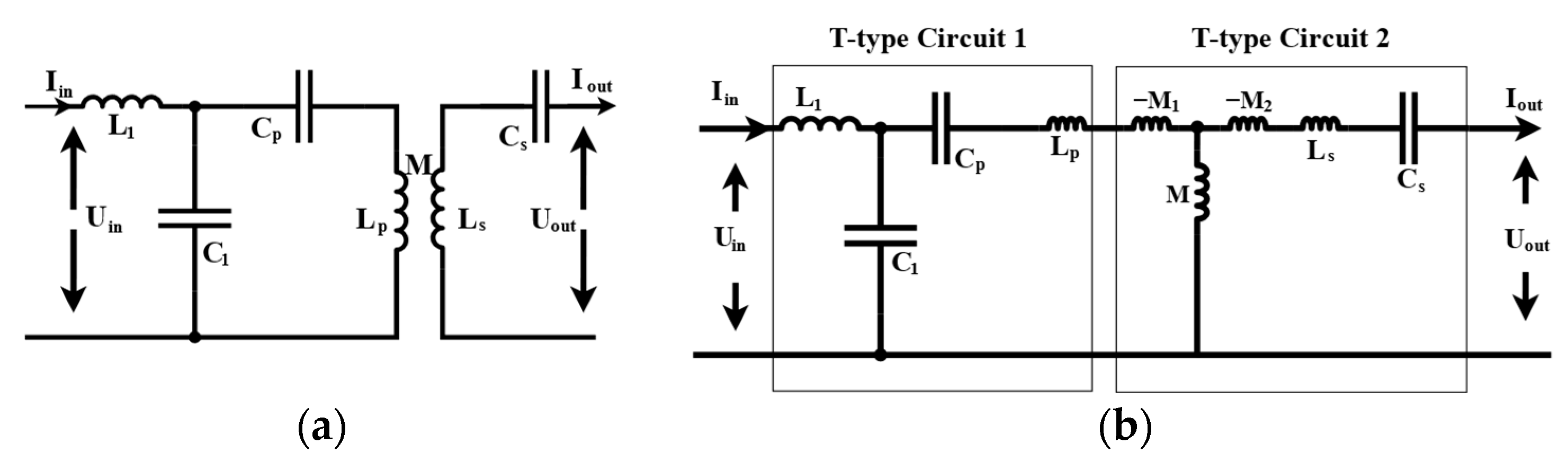
2.2. S-S Resonant Topology

The S-S resonant compensation topology model is depicted in Figure 3a, where the inductance of the coil is directly compensated by the capacitance which is connected in series with it [4]. Cp represents the primary side compensated capacitor and Cs represent the secondary side compensated capacitor. As shown in Figure 3b, the mutual inductance M of the symmetrical coil can be equated to a T-type circuit [22].
The relationship between its compensation capacitance and coil inductance is as follows.
ω 0 L s = 1 ω 0 C s
ω 0 L p = 1 ω 0 C p
ω 0 is the angular frequency of the system at resonance.
In Figure 3b, the impedances of Cp, Lp, and −M1 are equivalent to Z1 of the T-type circuit model. The impedance of −M2, Ls, and Cs are equivalent to Z2. The impedance of M is equivalent to Z3. As the S-S topology is equated to a T-type circuit at resonance, the topology functions as such, converting constant voltage input into constant current output.
According to Equation (1), CC output is:
I o u t 0 ( S - S ) = U i n j ω 0 M
Iout0(S-S) is the output current of the topology at resonance.
The equivalent impedance at resonance:
Z i n 0 ( S - S ) = ω 0 2 M 2 R e q
Zin0(S-S) is the input impedance.

2.3. LCCL-S Resonant Topology

The structure of the LCCL-S topology is shown in Figure 4a [23], and the equivalent circuit diagram for the LCCL-S topology could be found in Figure 4b. The coil is connected in series with the capacitor Cp, which equates to Z3 in a T-type circuit; this combination forms a T-type equivalent circuit with L1 and C1. The mutual inductance of the symmetrical coils is also equivalent to a T-type circuit. Therefore, the LCCL-S circuit would be equated to a cascade of two T-type circuits. The parameters of the T-type circuit equivalent of the mutual inductor cannot be changed, while the T-type circuit parameters of L1 can be freely designed.
The relationship between its compensation capacitance and coil inductance in LCCL-S topology is as follows.
ω 0 L 1 = 1 ω 0 C 1 = ω 0 L P 1 ω 0 C P
1 ω 0 C s = ω 0 L s
In T-type circuit 1, shown in Figure 4b, the impedance of L1 is equivalent to Z1 of the T-type circuit model, the impedance of Lp and Cp is equivalent to Z2, and the impedance of C1 is equivalent to Z3. In T-type circuit 2, the −M1 impedance is equivalent to Z1; the impedances of −M2, Ls, and Cs are equivalent to Z2 of the T-type circuit; and the impedance of M is equivalent to Z3. The LCCL-S topology is equated to two T-type circuits cascaded. Thus, T-type circuit 1 converts the CV input into a CC output, and T-type circuit 2 converts this CC output into a CV output again. According to Equations (1) and (2), the topology achieves a constant voltage output independent of the load.
For the CV output:
U o u t 0 ( L C C L - S ) = U i n M L 1
The relative positions between the transmitter coil and receiver coil are assumed to be unchanged in the transmitting process. Therefore, the mutual inductor M is a constant value. Thus, according to Equation (10), the gain of the output voltage Uout0 (LCCL-S) with respect to Uin can be varied by the parameters of T-type circuit 1 configured based on the value of L1. The equivalent impedance at resonance.
Z i n 0 ( L C C L - S ) = L 1 2 M 2 R e q
Uout0(LCCL-S) is the output current of the topology at resonance. Zin0(LCCL-S) is the input impedance.

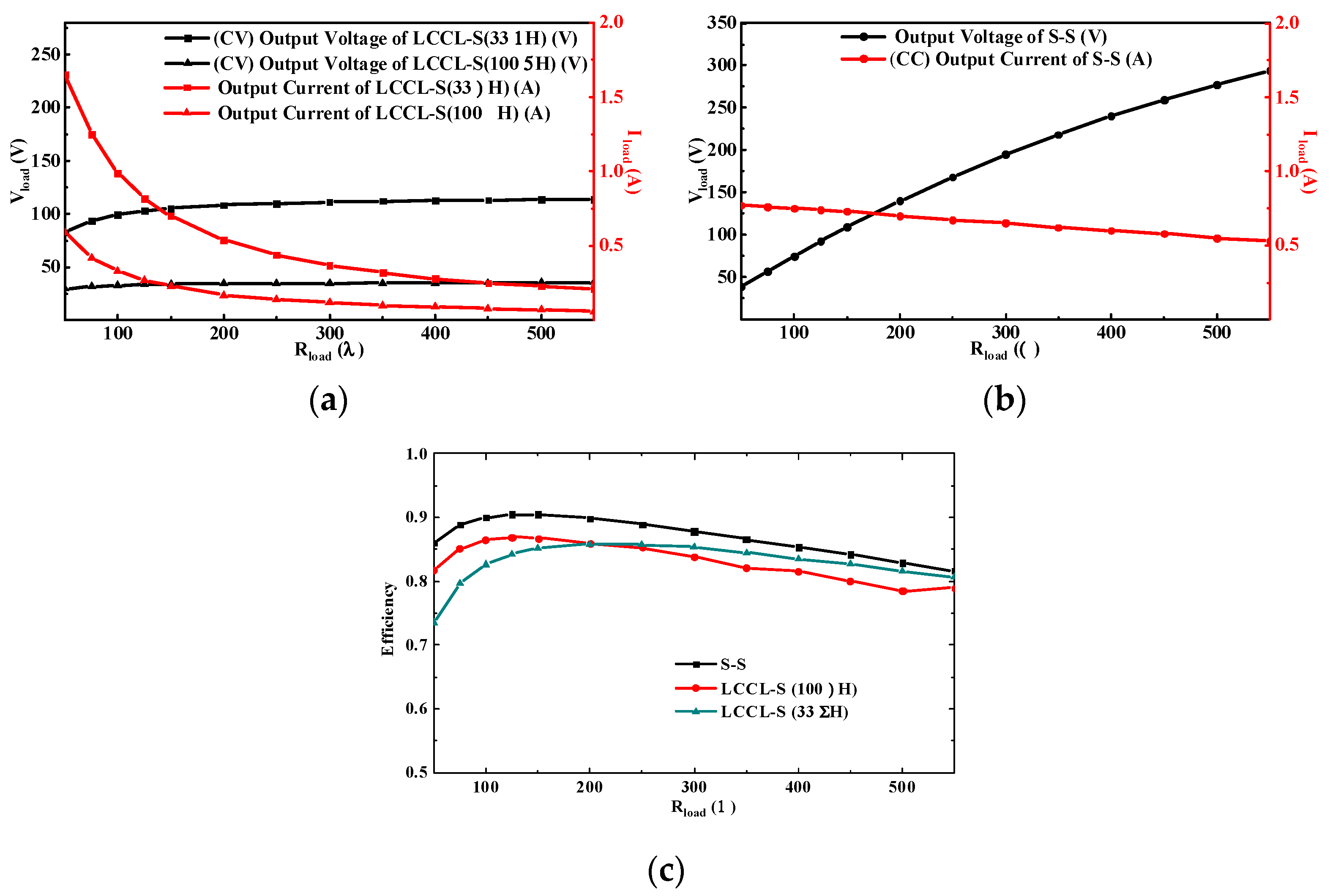
3. Experiment Verification

It is necessary to verify the feasibility of the WPT charging systems. Figure 5 shows the WPT prototype platform and cascade GaN-based FBI. The DC input sources (ITECH IT6526D) is used to supply high-level DC power to the WPT system. Auxiliary power supply (ITECH IT6721) is utilized to support DSP (TMS320F28335) and FBI. The DSP controller requires the input voltage to be 5 V and the FBI requires the constant voltage supply level to be 12 V. The programmable resistors choose ITECH DC electric load IT8816B to provide variable load resistors. The voltage and current measurements are used a current probe (Tektronix P5200A) and a differential voltage probe (Tektronix TCP2020) with an oscilloscope (Agilent DSOX2024A). FBI was formed by four Cascade GaN HEMT(TPH3206PS) and Silicon Carbide Schottky Diode (C3D08060A) are utilized to build the rectifier. The transmitter and receiver coil have the same size with outer diameter of 45 cm and an inner diameter of 30 cm formed with litz wire. The spacing between two coils is 12.5 cm. According to the model equation and experiment measurement result, the parameters of S-S and LCCL-S resonant compensation are shown in Table 1. To verify the relationship between the parameters of the resonant compensating inductor L1 and the voltage gain, the LCCL-S resonant topology with two set of parameters is designed.
To reduce the switching losses of the WPT system on the inverter, the Iin needs to lag behind the Uin by a small angle. In this way, the zero voltage switching (ZVS) is also realized [24]. Figure 6a–c show the output voltage (Uin) phase leads output current (Iin) of the FBI. Figure 6d–f show the Vds and Vgs for transistor S4 in FBI, demonstrating that Vds has dropped to zero before Vgs rises.
The DC supply voltage is used to 50 V and the load resistance is varied from 50 Ω to 550 Ω by a programmable load. Experimental data for CC and CV models with different resonant compensation topologies are shown in part a and part b of Figure 7. Simultaneously, the efficiency of the WPT system with different topologies is shown in part c of Figure 7. S-S topology is used to implement CC Mode and LCCL-S is used to implement CC Mode. For the LCCL-S structure, the experimental results demonstrate the relationship between the magnitude of L1 and the system mutual inductance M allows the output voltage to be achieved above or below the input voltage. When L1 is greater than the mutual inductance M, the voltage gain will be less than 1; when L1 is less than the M, the voltage gain will be greater than 1. According to Equation (10), the output voltage of the LCCL-S (33 μH) is 121 V for a DC input voltage of 50 V, which is approximately 113 V in the actual test. The output voltage of the LCCL-S (100 μH) is 40 V, which is approximately 35 V in the experimental result.
Figure 6a,b shows the output voltage and current for two LCCL-S topologies with different compensated inductors L1 as well as for the S-S topology. For example, the output voltage and current for the two LCCL-S topologies are 35.05 V, 0.12 A (100 μH), and 112.16 V, 0.37 A (33 μH) and the S-S topology voltage and current are 194.79 V, 0.65 A, for a load resistance equal to 300 Ω. As can be seen in Figure 7a, the output voltage variation rates for the two LCCL-S topologies are 2.6% (100 μH) and 4.8% (33 μH) for load resistances greater than 200 Ω, giving a good constant voltage output performance. Figure 7b shows that the S-S topology has a current variation of 7.9% at loads of 75–200 Ω. At loads above 200 Ω, the constant current performance deteriorates, and the output voltage is extremely high. This can cause damage to devices such as rectifier diodes. Figure 7c shows the variation in efficiency of the three topologies over a wide load range. The topology efficiency rises and then falls as the load resistance changes, with the S-S topology reaching a maximum efficiency of 90.46% at 150 Ω. The LCCL-S (100 μH) reaches a maximum efficiency of 86.92% at 125 Ω. The LCCL-S (33 μH) reaches a maximum efficiency of 85.79% at 200 Ω. However, the LCCL-S topology is the better choice for load ranges above 200 Ω and where a constant voltage output is required. It can also be seen from Figure 7c that the LCCL-S topology with a small compensating inductor is slightly more efficient for load resistances above 200 Ω.
Both the S-S and LCCL-S topologies maintain a high level of efficiency over a wide range of load variations. The overall efficiency of the LCCL-S topology is lower than that of the S-S topology as the LCCL-S topology has more passive components than the S-S topology. For the LCCL-S structure, two group parameters are necessary to be compared. An LCCL-S system with an L1 value of 100 μH will have a higher efficiency than a system with an L1 value of 33 μH for a load range of less than 200 Ω. At larger loads, the topology with an L1 value of 33 μH generates a larger current on the primary side coil, causing larger losses. In a load range greater than 200 Ω, the efficiency of an LCCL-S WPT system with an L1 value of 100 μH will be lower than an LCCL-S WPT system with an L1 value of 33 μH. The possible reason for this analysis is that the losses generated by the rectifier account for a larger proportion of the overall losses due to the smaller voltage gain of the topology with an L1 value of 100 μH.

4. Conclusions

In this paper, equivalent circuit models for the S-S and LCCL-S topology are analyzed. The expressions for the output voltage, current and input impedance are derived. The relationship between the output voltage and inductor L1 is investigated for the LCCL-S topology. The parameters of the S-S and the LCCL-S topology are specified for the ZVS based on the parameters of the transmission coil and the implementation condition. Two different LCCL-S systems are also developed to verify the relationship between the L1 inductance value and the mutual inductance M. Under a DC voltage input of 50 V, both topologies achieve ZVS. In the S-S topology, with the load range of 75–200 Ω, it achieves a maximum efficiency of 90.45%. In the LCCL-S topology (100 μH), with the load range of 200–550 Ω, it achieves a maximum efficiency of 85.94%. In the LCCL-S topology (33 μH), with the range of 200–550 Ω, it achieves a maximum efficiency of 85.79%. The output voltage and current also demonstrate that the different topologies accomplish the corresponding CC and CV functions. With a load resistance of 75–200 Ω, the S-S current varies by 7.9%. With a load resistance greater than 200 Ω, the voltage variation is 4.8% for the LCCL-S with a compensating inductor L1 of 100 μH and 2.6% for the L1 equal to 33 μH. Two sets of LCCL-S WPT systems obtained special voltage gain. Therefore, the parameter optimization of the LCCL-S WPT system would achieve different voltage gains for same transmitter coil and it is suitable for wide load variation. When the load resistance is equal to 300 Ω, the voltage gain is 0.7 for the LCCL-S with a compensating inductor of 100 μH and 2.22 for the LCCL-S with a compensating inductor of 33 μH.

Author Contributions

Conceptualization, Y.Z. (Yuhao Zhu) and H.W.; methodology, Y.Z. (Yuhao Zhu) and H.W.; investigation, Y.Z. (Yuhao Zhu); formal analysis, H.W.; writing—original draft preparation, Y.Z. (Yuhao Zhu) and H.W.; writing—review and editing, F.L., Y.Z. (Yongsheng Zhu) and W.L; supervision, W.L. and Y.P.; project administration, W.L.; funding acquisition, W.L. All authors have read and agreed to the published version of the manuscript.

Funding

This work was supported in part by the Suzhou Science and Technology program under Grant SYG201923 and SYG202131; in part by the Key Program Special Fund in Xi’an Jiaotong–Liverpool University (XJTLU) under Grant KSF-T-07.

Conflicts of Interest

The authors declare no conflict of interest.

References

  1. Feng, H.; Tavakoli, R.; Onar, O.C.; Pantic, Z. Advances in High-Power Wireless Charging Systems: Overview and Design Considerations. IEEE Trans. Transp. Electrif. 2020, 6, 886–919. [Google Scholar] [CrossRef]
  2. Kan, T.; Zhang, Y.; Yan, Z.; Mercier, P.P.; Mi, C.C. A rotation-resilient wireless charging system for lightweight autonomous underwater vehicles. IEEE Trans. Veh. Technol. 2018, 67, 6935–6942. [Google Scholar] [CrossRef]
  3. Mahesh, A.; Chokkalingam, B.; Mihet-Popa, L. Inductive Wireless Power Transfer Charging for Electric Vehicles–A Review. IEEE Access 2021, 9, 137667–137713. [Google Scholar] [CrossRef]
  4. Wang, C.S.; Stielau, O.H.; Covic, G.A. Design considerations for a contactless electric vehicle battery charger. IEEE Trans. Ind. Electron. 2005, 52, 1308–1314. [Google Scholar] [CrossRef]
  5. Aubakirov, R.R. Comparison of the geometry of the optimized coil pair of wireless power transmission systems with SS and SP compensation. In Proceedings of the 2021 IEEE Conference of Russian Young Researchers in Electrical and Electronic Engineering (ElConRus), St. Petersburg, Russia, 26–29 January 2021; pp. 2783–2786. [Google Scholar] [CrossRef]
  6. Yao, Y.; Wang, Y.; Liu, X.; Lin, F.; Xu, D. A Novel Parameter Tuning Method for a Double-Sided LCL Compensated WPT System With Better Comprehensive Performance. IEEE Trans. Power Electron. 2018, 33, 8525–8536. [Google Scholar] [CrossRef]
  7. Kavimandan, U.D.; Galigekere, V.P.; Onar, O.; Mohammad, M.; Ozpineci, B.; Mahajan, S.M. The Sensitivity Analysis of Coil Misalignment for a 200-kW Dynamic Wireless Power Transfer System with an LCC-S and LCC-P Compensation. In Proceedings of the 2021 IEEE Transportation Electrification Conference & Expo (ITEC), Chicago, IL, USA, 21–25 June 2021; pp. 1–8. [Google Scholar] [CrossRef]
  8. Chen, Y.; Zhang, H.; Park, S.-J.; Kim, D.-H. A Comparative Study of S-S and LCCL-S Compensation Topologies in Inductive Power Transfer Systems for Electric Vehicles. Energies 2019, 12, 1913. [Google Scholar] [CrossRef] [Green Version]
  9. Vu, V.B.; Tran, D.H.; Choi, W. Implementation of the constant current and constant voltage charge of inductive power transfer systems with the double-sided LCC compensation topology for electric vehicle battery charge applications. IEEE Trans. Power Electron. 2018, 33, 7398–7410. [Google Scholar] [CrossRef] [Green Version]
  10. Li, S.; Li, W.; Deng, J.; Nguyen, T.D.; Mi, C.C. A Double-Sided LCC Compensation Network and Its Tuning Method for Wireless Power Transfer. IEEE Trans. Veh. Technol. 2015, 64, 2261–2273. [Google Scholar] [CrossRef]
  11. Chen, Y.; Zhang, H.; Shin, C.-S.; Jo, C.-H.; Park, S.-J.; Kim, D.-H. An Efficiency Optimization-Based Asymmetric Tuning Method of Double-Sided LCC Compensated WPT System for Electric Vehicles. IEEE Trans. Power Electron. 2020, 35, 11475–11487. [Google Scholar] [CrossRef]
  12. Li, W.; Zhao, H.; Deng, J.; Li, S.; Mi, C.C. Comparison Study on SS and Double-Sided LCC Compensation Topologies for EV/PHEV Wireless Chargers. IEEE Trans. Veh. Technol. 2016, 65, 4429–4439. [Google Scholar] [CrossRef]
  13. Li, Y.; Zhu, Y.; Liu, W.; Wen, H.; Zhao, C.; Zhu, Y.; Pei, Y. High Efficiency WPT System for Electric Vehicles with LCL-S and SS compensation. In Proceedings of the 2019 IEEE 4th International Future Energy Electronics Conference, IFEEC, Singapore, 25–28 November 2019. [Google Scholar] [CrossRef]
  14. Rezk, T.M.; Fahmy, G.A.; Ibrahim, S.A.; Ragai, H.F. Design of a differential pow-er oscillator for 433 MHz WPT using e-GaN HEMTs. Ain Shams Eng. J. 2022, 13, 101581. [Google Scholar] [CrossRef]
  15. Qian, H.; Zhu, Y.; Deng, G.; Liu, W.; Chen, D.; Pei, Y. Cascode GaN Power Device and Its Application in Wireless Power Transmission System. J. Power Supply 2019, 17, 38–43. [Google Scholar] [CrossRef]
  16. Hu, J.S.; Lu, F.; Zhu, C.; Cheng, C.Y.; Chen, S.L.; Ren, T.J.; Mi, C.C. Hybrid Energy Storage System of an Electric Scooter Based on Wireless Power Transfer. IEEE Trans. Ind. Inform. 2018, 14, 4169–4178. [Google Scholar] [CrossRef]
  17. Vitols, K.; Poiss, E. Development of electric scooter battery pack management system. In Proceedings of the 2018 IEEE 59th International Scientific Conference on Power and Electrical Engineering of Riga Technical University (RTUCON), Riga, Latvia, 12–13 November 2018; pp. 1–5. [Google Scholar] [CrossRef]
  18. Laha, A.; Jain, P. Maximizing efficiency while maintaining voltage regulation of wireless power transfer systems using a buck-boost converter. In Proceedings of the 2021 IEEE Applied Power Electronics Conference and Exposition (APEC), Phoenix, AZ, USA, 14–17 June 2021; pp. 700–705. [Google Scholar] [CrossRef]
  19. Zhang, W.; Mi, C.C. Compensation Topologies of High-Power Wireless Power Transfer Systems. IEEE Trans. Veh. Technol. 2016, 65, 4768–4778. [Google Scholar] [CrossRef]
  20. Li, Y.; Hu, J.; Li, X.; Cheng, K.-W.E. A Flexible Load-Independent Multi-Output Wireless Power Transfer System Based on Cascaded Double T-Resonant Circuits: Analysis, Design and Experimental Verification. IEEE Trans. Circuits Syst. I Regul. Pap. 2019, 66, 2803–2812. [Google Scholar] [CrossRef]
  21. Lu, J.; Zhu, G.; Lin, D.; Zhang, Y.; Jiang, J.; Mi, C.C. Unified Load-Independent ZPA Analysis and Design in CC and CV Modes of Higher Order Resonant Circuits for WPT Systems. IEEE Trans. Transp. Electrif. 2019, 5, 977–987. [Google Scholar] [CrossRef]
  22. Ali, E.M.; Alibakhshikenari, M.; Virdee, B.S.; Soruri, M.; Limiti, E. Efficient Wireless Power Transfer via Magnetic Resonance Coupling Using Automated Impedance Matching Circuit. Electronics 2021, 10, 2779. [Google Scholar] [CrossRef]
  23. Feng, H.; Cai, T.; Duan, S.; Zhao, J.; Zhang, X.; Chen, C. An LCC-Compensated Resonant Converter Optimized for Robust Reaction to Large Coupling Variation in Dynamic Wireless Power Transfer. IEEE Trans. Ind. Electron. 2016, 63, 6591–6601. [Google Scholar] [CrossRef]
  24. Li, G.; Kim, D.-H. A wireless power transfer charger with hybrid compensation topology for constant current/voltage onboard charging. Appl. Sci. 2021, 11, 7569. [Google Scholar] [CrossRef]
Figure 1. Block diagram of LCCL-S WPT system.
Electronics 11 00420 g001
Figure 2. T-type circuit model.
Electronics 11 00420 g002
Figure 3. (a) S-S resonant compensation topology, (b) Equivalent circuit for S-S topology.
Electronics 11 00420 g003
Figure 4. (a) LCCL-S resonant compensation topology, (b) Equivalent circuit for the LCCL-S topology.
Electronics 11 00420 g004
Figure 5. (a) Experimental platform of proposed WPT system, (b) Cascade GaN based high frequency full bridge inverter.
Electronics 11 00420 g005
Figure 6. FBI output current/voltage waveformes and ZVS condition of (a,d) LCCL-S with L1 = 33 μH, (b,e) LCCL-S with L1 = 100 μH, and (c,f) S-S.
Electronics 11 00420 g006
Figure 7. Experimental results for (a) CV model with two sets of LCCL-S resonant compensation circuits and (b) CC model with S-S resonant compensation topology. (c) The efficiency of the WPT system with different topologies.
Electronics 11 00420 g007
Table 1. Parameters of S-S and LCCL-S resonant compensation.
ParametersS-SLCCL-S
(L1 = 33 μH)
LCCL-S
(L1 = 100 μH)
System Frequency f0100 kHz100 kHz100 kHz
Coil self-inductances Lp, Ls385 μH385 μH385 μH
Coil mutual-inductances M80 μH80 μH80 μH
Primary compensation inductance L1\33 μH100 μH
Primary parallel capacitance C1\76 nF25.33 nF
Primary series capacitance Cp6.6 nF7.19 nF8.89 nF
Secondary series capacitance Cs6.6 nF6.6 nF6.6 nF
Publisher’s Note: MDPI stays neutral with regard to jurisdictional claims in published maps and institutional affiliations.

