Article

FPSNET: An Architecture for Neural-Network-Based Feature Point Extraction for SLAM

School of Integrated Circuits, Tsinghua University, Haidian District, Beijing 100084, China
*
Author to whom correspondence should be addressed.
Electronics 2022, 11(24), 4168; https://doi.org/10.3390/electronics11244168
Submission received: 26 October 2022 / Revised: 22 November 2022 / Accepted: 8 December 2022 / Published: 13 December 2022
(This article belongs to the Section Artificial Intelligence Circuits and Systems (AICAS))

Abstract

:
The hardware architecture of a deep-neural-network-based feature point extraction method is proposed for the simultaneous localization and mapping (SLAM) in robotic applications, which is named the Feature Point based SLAM Network (FPSNET). Some key techniques are deployed to improve the hardware and power efficiency. The data path is devised to reduce overall off-chip memory accesses. The intermediate data and partial sums resulting in the convolution process are stored in available on-chip memories, and optimized hardware is employed to compute the one-point activation function. Meanwhile, address generation units are used to avoid data overlapping in memories. The proposed FPSNET has been designed in 65 nm CMOS technology with a core area of 8.3 mm2. This work reduces the memory overhead by 50% compared to traditional data storage for activation and overall by 35% for on-chip memories. The synthesis and simulation results show that it achieved a 2.0× higher performance compared with the previous design while achieving a power efficiency of 1.0 TOPS/W, which is 2.4× better than previous work. Compared to other ASIC designs with close peak throughput and power efficiency performance, the presented FPSNET has the smallest chip area (at least 42.4% reduction).

1. Introduction

Simultaneous localization and mapping (SLAM) has become one of the major research topics with the fast development of robotics. SLAM is the technology enabling the robot to locate itself and construct the map of the surrounding environment [1,2]. For the SLAM algorithms based on feature points, the extraction of feature points and the corresponding descriptors is a vital procedure that largely influences the performance of the whole system [3]. Different feature points and descriptors have been proposed, including SURF [4], ORB [5], and SIFT [6]. Various SLAM systems are based on these traditional feature point extraction algorithms. However, they may fail to provide consistent feature detection and associated results in complex environments. In comparison, feature extraction based on deep convolutional neural networks (CNNs) has replaced the hand-crafted features for SLAM-related research and applications. Recently, SuperPoint based on CNN was proposed for feature point extraction and it outperformed the traditional algorithms in both accuracy and stability [7]. It is suggested as an alternative for patch-based neural networks that work on a fully convolutional model on full-sized images and jointly compute pixel-level interest point locations and associated descriptors. Other CNN-based methods also present a significant improvement in feature extraction and descriptor generation such as DeepDesc [8] and GeM [9]. However, CNN has a much higher computational complexity and it requires more memory footprint. The computation of SuperPoint is time- and resource-consuming, making it hard to implement on mobile devices such as robots and unmanned aerial vehicles (UAVs). Considering these constraints, an area- and power-efficient hardware accelerator architecture with a reduced memory footprint toward the ASIC (application-specific integrated circuit) implementation is proposed in this work, which we call FPSNET. It supports SuperPoint for feature point extraction in SLAM.
Various neural-network-based accelerators have been presented in recent years aiming for robotics and vision [10,11,12]. In the hardware aspect, an FPGA-based accelerator for SuperPoint was given in [13], which tried to optimize the activation function and normalization. In other work, based on the SuperPoint, an FPGA-based real-time keypoint extraction hardware accelerator through algorithm-hardware co-design for mobile VSLAM applications is proposed, which improves the processing speed while maintaining high accuracy [14]. The design of Ref. [15] achieved a fast and energy-efficient FPGA implementation of the feature extraction algorithm with effective local search. Over the years, some ASIC-based CNN accelerators have been presented in the literature [16,17,18,19,20,21,22]. However, to the best of our knowledge, we are the first to design ASIC for deep-neural-network-based feature point extraction for SLAM.
To implement the neural-network-based feature point extraction for SLAM, a few implementation problems require solutions in terms of hardware optimizations. The data path optimization is critical due to the large neural network size (∼46 GOPS for image resolution of 480 × 640) of SuperPoint. There is a large transmission of data between off-chip and on-chip memories. In [23,24,25,26,27], the CNN accelerators optimized the data path using loop unrolling and tiling for the enhanced performance of the convolution layer. Meanwhile, they managed to store intermediate results and partial sums, resulting in a process of convolution in extra memory registers, line buffers, or on-chip memories to reduce the off-chip data movement. The input size to every convolution layer is large, and therefore the memory constraint is strict and it is hard to store all the data in on-chip memory. Therefore, a pipelined architecture with reduced hardware resources is required to optimize the data path to restrict off-chip movement and extra on-chip storage. Considering the data storage, the traditional ping-pong buffer technique is an overhead in terms of memory consumption because it uses disjunctive memory space [28]. On-chip static random access memory (SRAM) is dominant for CNN accelerator designs [29]. Therefore, the reduction of memory size ultimately reduces the chip area and, consequently, chip cost. Meanwhile, due to large memory size, static power and energy consumption increase by a factor of 25× times due to the processing of fetched data [30,31]. The work in [28] advised the overlapped method for activation layers’ data rather than the traditional ping-pong buffering technique. However, it still requires extra memory to store overlapped data.
In this article, FPSNET handles the complex data flow by allowing the reuse of data efficiently. Memory architecture and data storage techniques are employed to reduce memory size and storage devices. ReLU operation is implemented to avoid the partial sum storage to off-chip memory. Therefore, the FPSNET accelerator mainly has the following four key innovations.
  • A new convolution layer data flow is implemented to manage the streaming data using a row-based feature processing.
  • An individual state controller (SC) and the bus arbiter and decoder module are deployed.
  • A multi-bank memory system employing feature and synapse parallelism is designed to meet the data access demand, which avoids the traditional ping-pong buffer.
  • Hardware implementation of the ReLU activation function is optimized.
The FPSNET design achieved a 1.0 TOPS/W of power efficiency which is 2.4× higher compared to previous ASIC design [32]. Moreover, it reduces an overall 35% of memory consumption and the area is improved by 1.9× to implement the feature point extraction for the SLAM algorithm.
The rest of the paper is organized as follows. In Section 2, a background of SLAM, SuperPoint neural network, and parallelism employed in this work is explained. FPSNET architecture and data path flow are presented in Section 3, followed by proposed optimization techniques in Section 4. Experimental and simulation results are explained in Section 5, and the conclusion is given in Section 6.

2. SLAM Based on SuperPoint Neural Network

Figure 1 shows the key elements of an algorithm in our neural-network-based SLAM system. It shows that keypoint extraction using a SuperPoint neural network is implemented. The following section gives a brief overview of CNN-based SLAM and its architecture.

2.1. CNN-Based SLAM

SLAM has become a major research topic in robotics. It is an algorithm to make the robot aware of the surrounding environment and the position of itself, which is a basic ability of humans. Currently, the basic framework of SLAM has been well-developed with some widely applied algorithms such as ORB-SLAM [33], LSD-SLAM [34], and DF-SLAM [35]. Generally, a SLAM system includes three threads: tracking, local mapping, and closure detection. There are different algorithms for tracking thread, such as feature-point-based and optical-flow-based algorithms. The feature-point-based algorithms are the major method due to the high robustness in different illumination conditions. The first step of feature-point-based algorithms is to extract the feature points from the input frame. Then, by matching the feature points between different frames, the relative rotation and translation can be estimated. In previous research, different hand-crafted extraction methods have been applied. Although sufficient works based on those algorithms have proved their efficiency and reliability, there still exist different shortcomings of different algorithms. With the fast development of deep neural networks, convolutional neural networks are promising in the field of interest point extraction. SuperPoint based on CNN outperforms the previous works significantly [7].

2.2. SuperPoint Architecture

The architecture of the feature point extraction method using the SuperPoint convolutional neural network is presented in [7]. It works on full-sized images and generates interest point detections with fixed-length descriptors in a single forward pass. This is where the complexity of neural network lies. It is working on a full-sized image and an encoder is shared and used to reduce the image dimensions, as shown in Figure 2.
The encoder part uses a VGG-style [36] to downsample the input image. It consists of convolution layers, max-pooling, and nonlinear activation function, i.e., ReLU. The three max-pooling layers reduce the input image size of H i n × W i n to H o u t = H i n /8 and W o u t = W i n /8. The encoder maps the input image I H i n × W i n to an intermediate tensor of X H o u t × W o u t × F with smaller spatial dimensions but with greater channel depth F. The input image size to this architecture is H i n × W i n = 480 × 640 . The architecture consists of eight convolution layers and a kernel size (K) of 3 × 3 with three max-pooling layers after every two convolution layers (group of two convolution layers Conv1a, Conv1b, etc.). The features are changing as 64–64–64–64–128–128–128–128 with a window stride ( S k ) of one. Therefore, considering an input image of 480 × 640 resolution, the network size becomes too large as ∼46 GOPS and it is hard to run on CPU and even on GPU/FPGA due to large power consumption. To use fewer hardware resources, the whole network is quantized (Q bits) to a 16-bit fixed point to achieve the required performance without any significant loss in accuracy [37].

2.3. Parallelism in Convolutional Neural Network

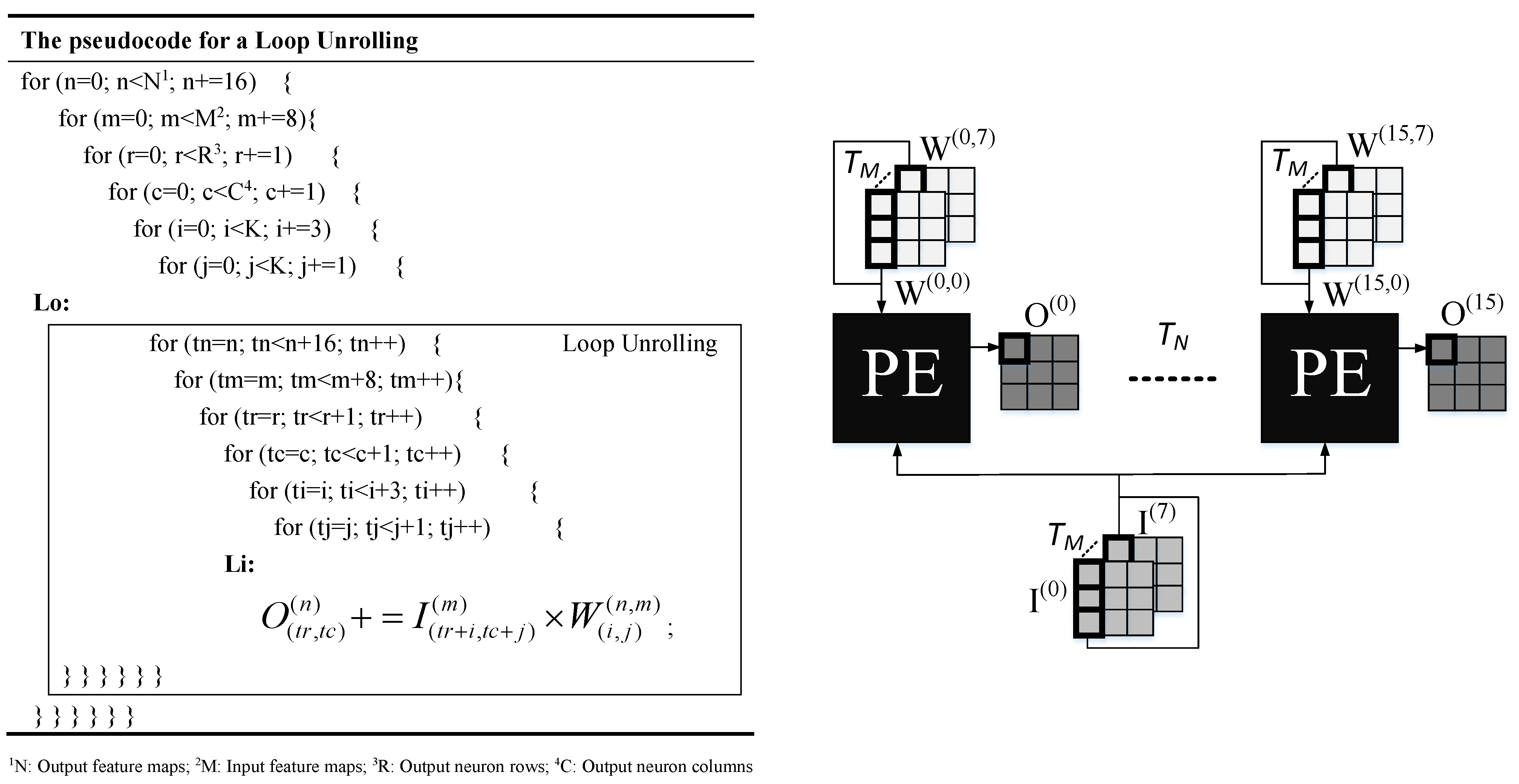
The basic computation in the encoder part of the SuperPoint neural network is the convolution of input feature maps with kernel weights. It is required to optimize the data path because it requires a huge amount of data transfer from off-chip to on-chip memories. Moreover, parallelism is also critical to acquire high throughput and use the limited hardware resources efficiently. Therefore, a data path is optimized in this work and it is explained in Section 3. The convolution layer can be unrolled and tiled as presented in [23,26]. Therefore, loop unrolling and tiling are performed in this work as shown in pseudocode of Figure 3, where τ = < T N , T M , T r , T c , T i , T j > is a set of unrolling factors. The loops which are marked by the inner box are unrolled to operate in parallel and the loops outside the inner box execute sequentially. Three types of parallelism can be achieved to different unrolling factors, which are as follows [19,26]:
  • The loops related to the feature map can be unrolled to T M and T N < T N , T M > factors. T M are input feature maps processed at the same time while generating T N output feature maps. This is called feature map parallelism (FP).
  • The loops for neurons are also unrolled with factors of < T r , T c > , where T r × T c of one output feature map are processed at the same time. It is called neuron parallelism (NP).
  • Synapse-related loops are also unrolled with factors < T i , T j > where T i × T j synapses of one kernel weight are computed in one processing step and called synapse parallelism (SP).
It is an ideal architecture that can support all of the abovementioned processing styles. However, it is not easy to utilize all of these parallelisms due to the different data flow in these processing styles. Therefore, in FPSNET, a multiple feature map, a single neuron, and multiple synapses (MFSNMS) are implemented with feature map and synapse parallelism. The feature map and synapse parallelism-related loops are unrolled with factors < T N = 16 , T M = 8 > and < T i = 3 , T j = 1 > , respectively, and neuron parallelism is taken as < T r = 1 , T c = 1 > . The final architecture on the basis of the abovementioned loops is shown in Figure 3. Therefore, at each clock cycle, T M input feature maps are convolved to generate T N output feature maps.

3. FPSNET Architecture and Data Path

3.1. Data Path Optimization for Pipelined Architecture

In [26], algorithm 1 shows the original loop computation to perform convolution in the convolution layer. To perform convolution efficiently, loop reordering and tiling have already been implemented by many researchers [23,25,26,27]. There is a problem with storing the entire intermediate results in on-chip or off-chip memories. Meanwhile, a doubled buffer scheme in [25,27] helped to pipeline the computation. However, there are problems of consuming a large number of on-chip RAMs when a network becomes deeper. Refs. [24,38,39,40,41] utilized off-chip storage for intermediate results to reduce the size of on-chip memories. Therefore, off-chip memory access slows the computation and also consumes more power.
In this design, the target is to eliminate the off-chip memory accesses for intermediate data and partial sum while reducing the on-chip SRAM. Similarly, pipelined architecture is applied to accommodate the streaming nature of data. Kernel weights are stored to on-chip SRAMs and are fully reused while activation data are changing at each clock cycle. The partial sum is stored to on-chip memories and fully reused partial sum to perform the ReLU activation function to generate output feature maps. Therefore, ReLU hardware optimization is implemented to efficiently reuse the partial sum. In this architecture, weights are fully reused by storing all the weights required for generating T N output feature maps, and input feature maps are partially reused for T M convolution. While shifting the convolution window towards F I N features, the next input feature maps ( T M ) are fetched from external memory to on-chip memory. Therefore, this operation repeats I t r = F I N / T M a number of times till the computations of all F I N features are completed.
The data flow implemented in this work is shown in Figure 4. The sliding cube of size ( K × 1 × T M ) from the input image slides along the width of an input image and it is called a row-based feature processing operation. This input sliding cube is convolved with T N number of weights every time to generate temporary T N output values. These weights are reused in a row-based feature processing operation till the columns reach a width of input image W i n . The input sliding cube then shifts T M channels and reaches towards the end of F I N features. These T N computations are performed in parallel and their partial sum is saved to on-chip memories to perform single-point ReLU operation after completion of all F I N features convolution. This process continues for the next change in a row till it completes the convolution of H i n input image. Optimized address generation logic in the output module is employed to efficiently perform the ReLU activation function by reusing the partial sum.
Considering the hardware resources, memory banks are required to provide the parallel data to T N number of processing elements (PEs). The memory size for the input image and kernel weights is dependent on the convolution layer number. However, the bit-width of each memory is of fixed size K × Q , where K is kernel size and Q is quantization bits of input image and weights. The depth of memory is dependent on the convolution layer number.

3.2. Architecture Overview

Figure 5 shows the FPSNET accelerator architecture for the SuperPoint neural network. It consists of registers for configuration, control, and status data. Bus arbitration is implemented for data bus handling and the decoder part is configured on the input address for the selection of memory banks and generation of required control signals. In this design, loop unrolling and tiling are employed with the factor of < T N = 16 , T M = 8 > . Input buffers consist of T M number of memories in a bank and they also consist of a finite-state controller to configure and manage the writing and reading of data from memories. The address generation unit (AGU) is designed to generate a reading address to efficiently manage the overlapped data. Similarly, weight buffers consist of T N memory banks and each memory bank contains T M number of memories. AGU manages to fully reuse kernel weights. Output buffers have T N number of memories and they store partial sums to memories that come from PE units. Optimized ReLU hardware is implemented to perform the activation function without sending intermediate data back to external memory. The overall architecture is designed for 16-bit fixed-point data.

3.3. Configuration Parameters

The configuration word is transferred to the chip from the external interface to the local register on a 64-bit data bus. The control register receives the control word which also includes the configuration information and commands. The configuration word information is shown in Table 1. The control register receives the configuration parameters as mentioned in Table 1 and transfers them to the configuration register. SpL command is reserved for the special convolution layer of the first input image of size 480 × 640 × 1 (one input feature).

3.4. Arbiter and Decoder

The arbiter executes the bus arbitration to manage the data flow from the output interface to internal on-chip memories and registers. Input data are received on a 64-bit data bus and memories are designed to store K × Q pixels at each memory location. Therefore, it requires 48 bits out of the 64-bit bus where the arbiter is handling the data and address bus. There is a 21-bit address ( A [ 20 : 0 ] ) bus and the decoder decodes and generates required control signals for AGUs in input, weights, and output buffer modules.
The lower 11 bits ( A [ 10 : 0 ] ) of the address bus are reserved for writing and reading of data to all memories. From A [ 20 : 11 ] , number of bits generate control signals for AGUs and the selection of each memory in independent module. The details about the individual address decoding are presented in Table 2.
Table 2 illustrates the address decoding for the decoder and it also shows the address range required for different memories and banks. For example, for each weight memory bank selection, the valid address A [ 17 : 14 ] range is 0000 to 1111, and within each memory bank, A [ 13 : 11 ] bits can select any memory out of a total T M memories.

3.5. Processing Element (PE) Design

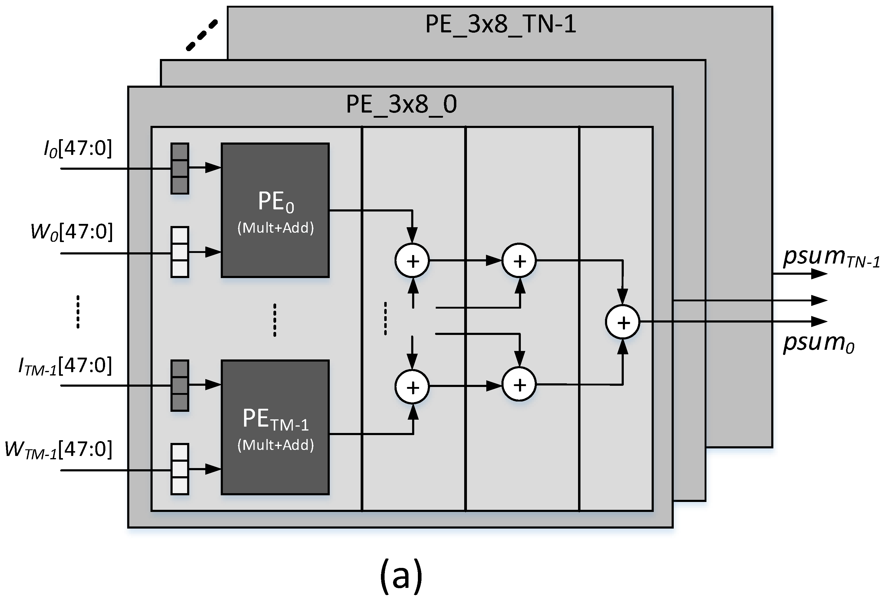
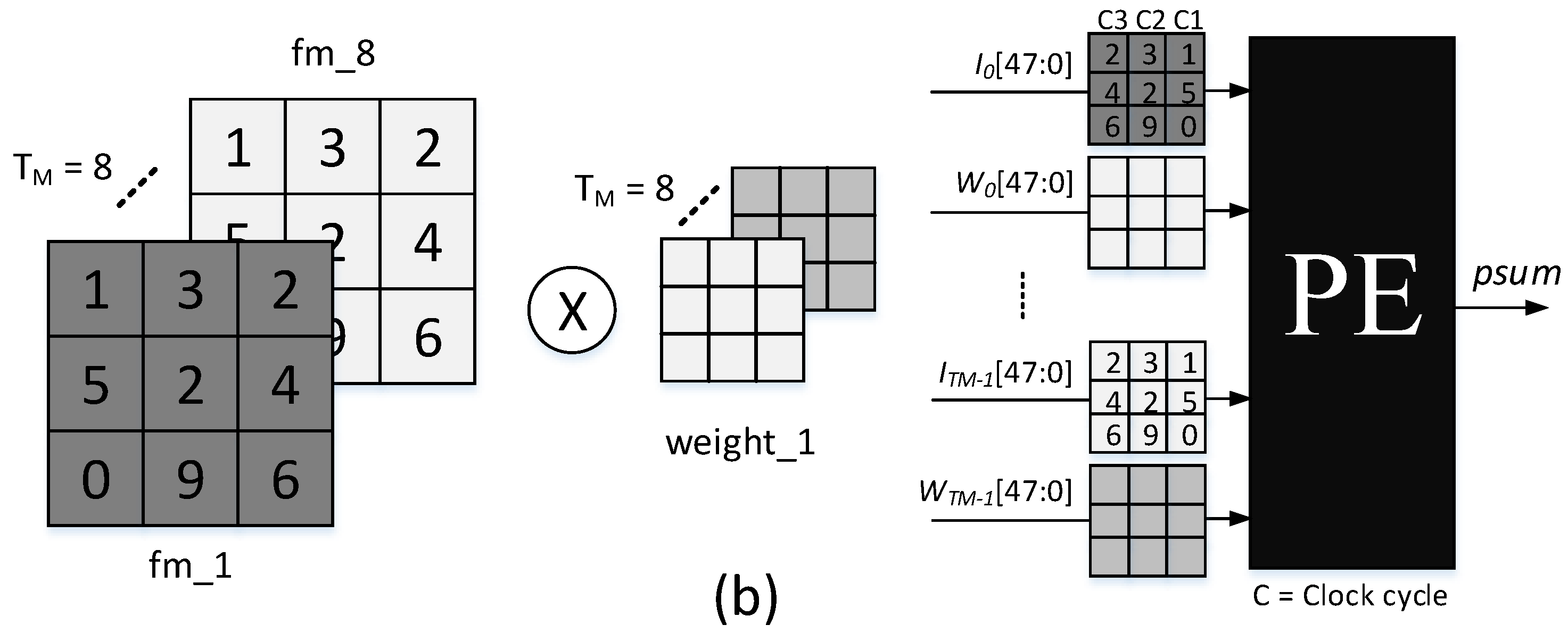
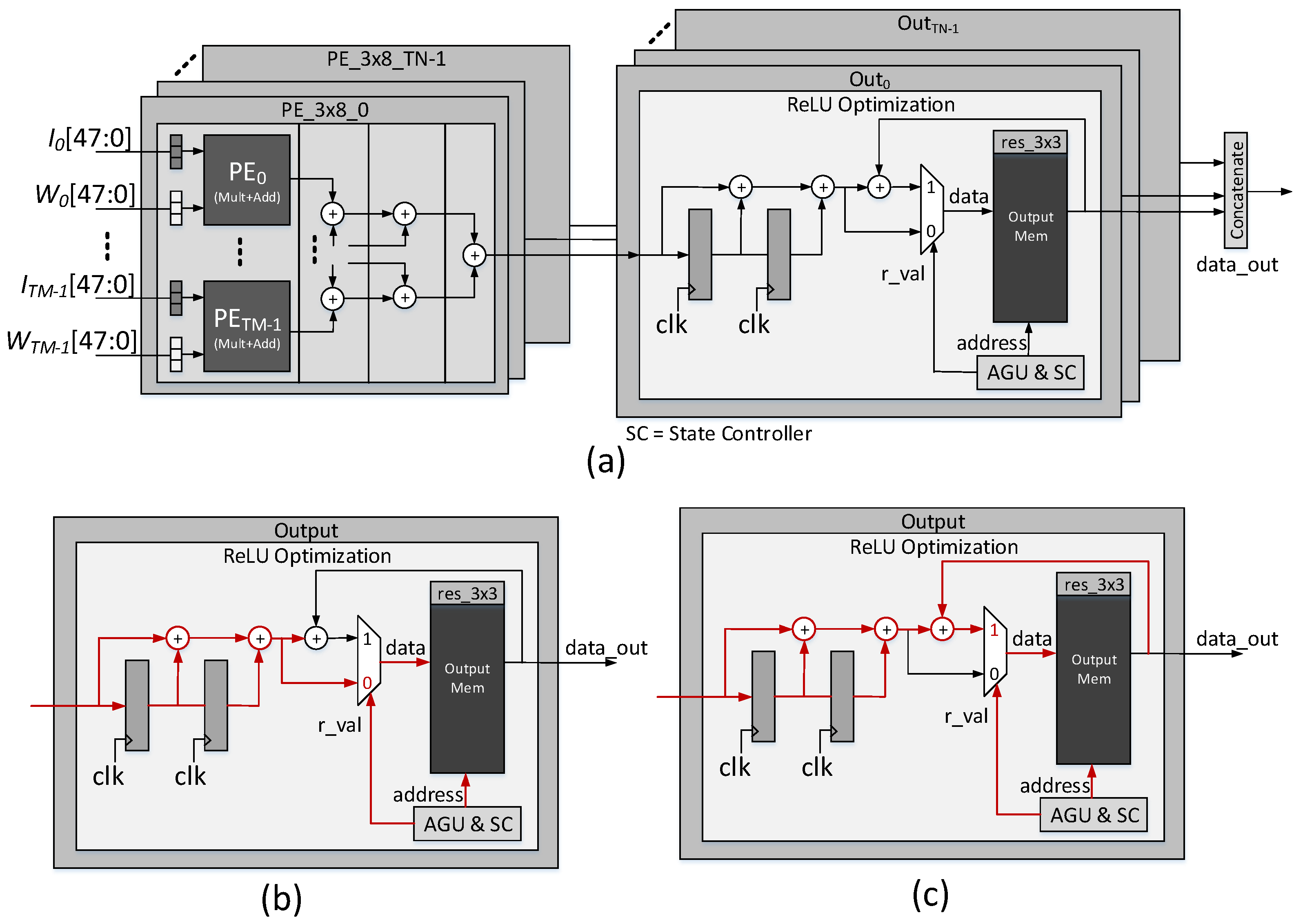
The processing element design is shown in Figure 6a. As discussed, the two feature-map-related loops are unrolled with a factor of < T N , T M > . At each clock cycle, this design handles the T M input to each PE unit and generates data for T N output feature maps in parallel. The number of PE units depends on the value of T N , and the input of each PE unit is based on T M , as shown in Figure 6a. Each PE unit design consists of ( K × T M ) multipliers and ( ( K × T M ) 1 ) adders. After initial latency, at every cycle, ( K × T M ) neurons and ( T N × K × T M ) synapses data are loaded. In each PE unit, they are multiplied and locally summed up to generate a partial sum. This output of partial sum is then saved into output on-chip memories and waits for the next data to come for further summation. Therefore, the number of clock cycles to complete T N neurons are equal to the size of K. This whole data flow to each PE unit is explained in Figure 6b. The PE unit is designed to have pipelined architecture, and the critical path is reduced to a delay of one multiplier and two adders. In each PE unit, there is a sub-PE unit to multiply the input of K inputs and sum the results for further addition to the top PE module. Therefore, the top PE unit receives the data from each sub-PE unit to generate the partial sum on ( K × T M ) inputs.
Figure 6. (a) Processing element (PE) unit design. (b) Processing element data flow.
Electronics 11 04168 g006aElectronics 11 04168 g006b

3.6. On-Chip Memory Architecture

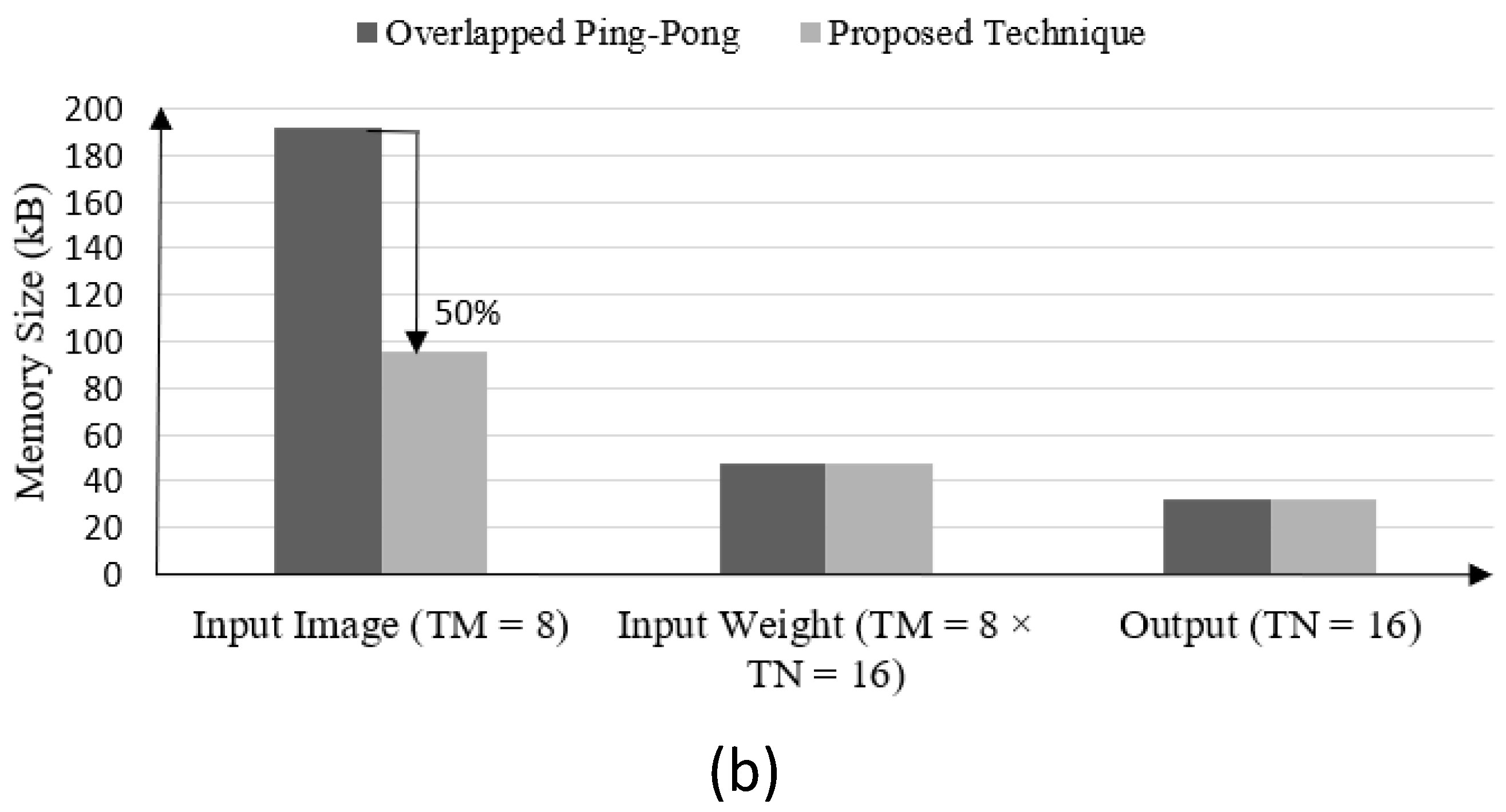
On-chip memory architecture is based on the unroll factor of < T N , T M > , as shown in Figure 5. Similarly, the memories are arranged to provide parallel data of ( K × T M ) neurons and ( T N × K × T M ) synapses to processing elements. Effective input image memory size is ( K × Q × ( W i n + 2 P ) × F c × T M ) , where P = number of zero padding and total memory size is 96 kB, because memory size depends on the number of address bits 2 x (x = number of address bits). Similarly, the weight memories are organized into T N memory banks and each memory bank contains T M number of memories. Therefore, the usable memory size for input weights is ( K × K × Q × F c × I t r N o × T N × T M ) . The actual memory size is 48 kB; output memory is arranged based on T N value, and memory size is ( Q × W i n × T N ) . Therefore, total output memories consist of 32 kB size. A total size of 176 kB is utilized as on-chip memory in this chip design.

4. Proposed Optimization Techniques

4.1. Data Arrangement in Memories

As explained in the previous section, the accelerator is based on unroll factor of < T N , T M > . Therefore, considering the input image memories, they depend on T M value and weight memories are placed according to ( T N × T M ) . The number of output memories is T N . The objective is to place activation data in memories to avoid overlapping and the traditional ping-pong storage technique. Further, the required data arrangement will help to compute the one-point ReLU activation function without transferring data to off-chip memories. Since the architecture is pipelined, after initial latency, results are computed at every clock cycle.
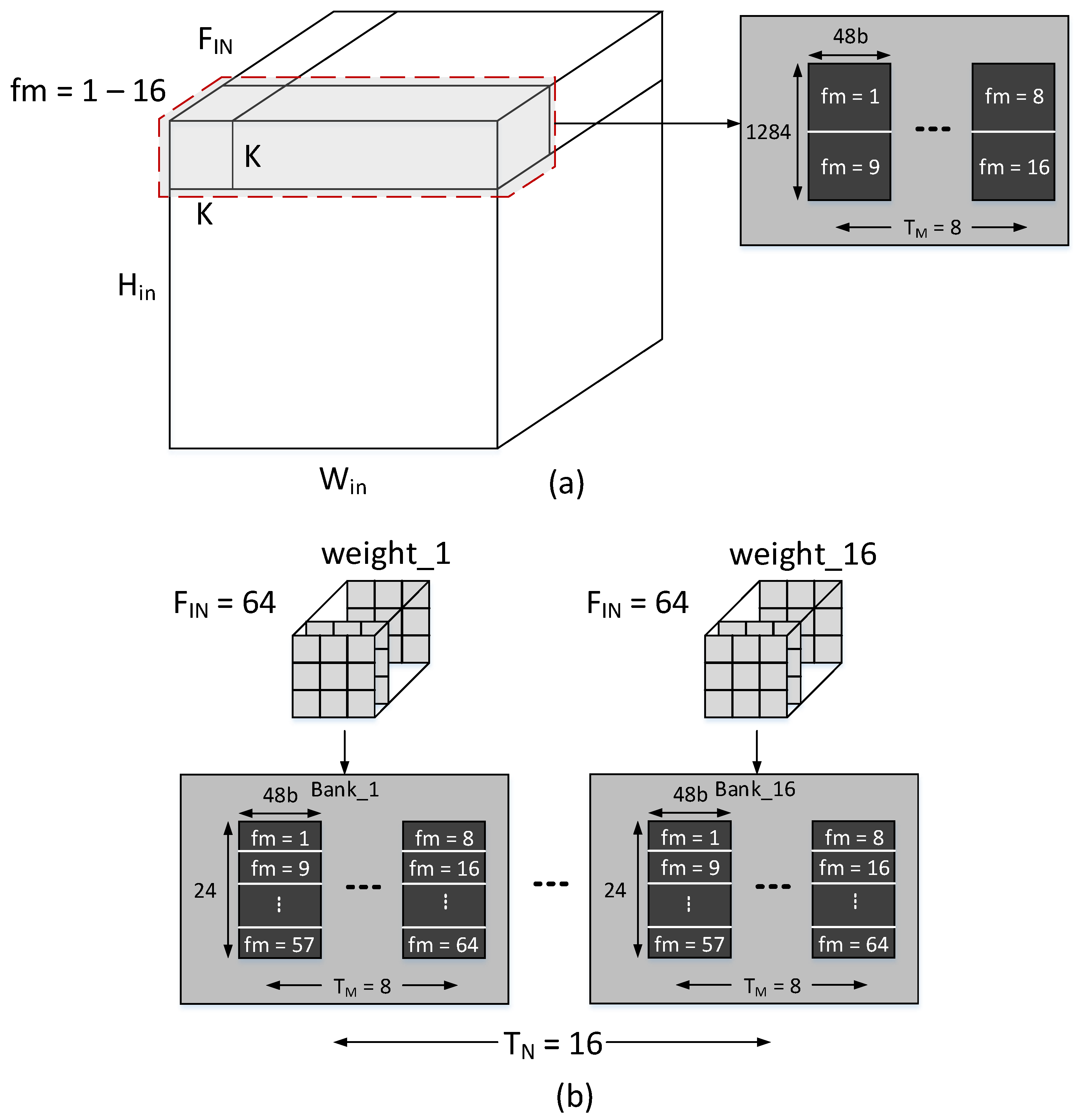
Each input and weight memory can store f m number of feature maps out of a total F I N input feature maps. In this design, a non-overlapped technique is proposed and implemented instead of the overlapped ping-pong technique. Therefore, more input features can be stored on-chip and it will reduce the memory transaction to off-chip memory. Figure 7a shows the data arrangement for an input image where, out of F I N = 64 features maps, f m = 16 number of input feature maps are stored to on-chip memories for Conv1b layer as an example. Meanwhile, in each memory, at a time, two f m ( F c = 2 ) are stored as depicted in Figure 7a. Similarly, Figure 7b shows the data arrangement for input weights. As compared to input features, all weights of T N numbers are stored in on-chip memories to avoid external memory access, and weights are fully reused for the entire convolution for T N output features. To implement the proposed data arrangement technique, the AGU becomes complex to manage the overlapping of data for activations.
Table 3 presents the parameters of the input image and weights for each convolution layer for the SuperPoint neural network. In all convolution layers, padding (P) is true and F c shows a total number of input features stored in each memory. H i n and W i n are the height and width of an input image. The iteration number and memory locations required for each memory are calculated as follows:
I m e m = ( W i n + 2 P ) × F c
I t r N o = F I N / ( T M × F c )
F I N and F O U T are input and output feature numbers, respectively, for each convolution layer. The iteration count I t r N o shows that a maximum number of iterations is required to complete convolution for all F i n features. The number of memory locations required to store all input weights can be computed as follows:
W m e m = K × F c × I t r N o

4.2. Address Generation Unit (AGU)

The independent AGU helps to generate an address for reading data of input features and weights. The AGU of the output module incorporates both read and write operations for special ReLU hardware implementation.
An AGU for input feature maps is designed to prevent extra storage required for overlapped data in the traditional ping-pong technique. When K × K window shifts by a factor of stride S k , there are overlapped data for input image and also intermediate results which require extra on-chip storage or off-chip movement [23,24,25,26,27,38,39,40,41]. In Figure 8, it can be observed that overlap data are unnecessarily written to on-chip memory to make the address generation logic simple with extra overhead of on-chip memory. To avoid this data arrangement, in this work, an optimized AGU logic is implemented to manage the overlapping. The data are written normally with consecutive write without writing overlapped data to memories, as depicted in Figure 8. However, to read the required data, AGU logic becomes complex but a considerable amount of memory is saved.
The AGU logic for reading an input image is shown in Algorithm 1. The final formula is given below after generating the required parameters for read address.
A i = ( S k × A p ) + O s
where
A p = A p + 1 , if ( O s = 2 ) 0 , otherwise ,   a n d O s = 0 , if ( O s = 2 ) O s + 1 , otherwise
where A i = image read address, S k = stride value, A p = address pointer, and O s = offset address.
Algorithm 1 AGU for input image reading.
Require: v a l i d 0 , 1
Require: S k : stride
1: O s 0  
2: A p 0  
3:while v a l i d 0 doValid signal from SC
4:     O s O s + 1  
5:     if O s = 2 then 
6:         O s 0  
7:     end if 
8:end while 
   
9:for i 0 , I m e m 1 do 
10:     if O s = 2 then 
11:         A p A p + 1  
12:     else 
13:         A p A p  
14:     end if 
15:end for 
16: A i ( S k × A p ) + O s  
Similarly, to provide the exact input weight for convolution with the input image, address generation logic is required because all weights are stored in on-chip memories. Algorithm 2 shows the address generation logic for weights. The formula to generate the required read address is given below:
A w = ( 3 × F c × I t r N o ) + ( 3 × F m ) + O s
where
F m = F m + 1 , if ( j = ( W m e m / F c ) ) F m , otherwise
where A w = weight read address, F m = current feature map for processing (i.e., 0, 1, ..., 15), i = {0, 1, ...( I m e m 1)}, and j = {0, 1, ...( W m e m 1)}.
Algorithm 2 AGU for input weights reading.
Require: v a l i d 0 , 1
Require: I t r N o : Iteration Number
Require: F c : Feature Count
1: O s 0
2: F m 0
3: P o 1
4:while v a l i d 0 do
5:     O s O s + 1
6:     if O s = 2 then
7:         O s 0
8:     end if
9:end while
  
10:for j 0 , W m e m 1 do
11:     if j = ( ( W m e m / F c ) × P o ) then
12:         F m F m + 1
13:         P o P o + 1
14:     else if j = W m e m then
15:         F m 0
16:         P o 0
17:     end if
18:end for
19: A w = ( 3 × F c × I t r N o ) + ( 3 × F m ) + O s

4.3. Memory Optimization

As discussed in the previous section, the AGU manages the overlapped data to prevent extra storage required for the temporary storage of data. The traditional ping-pong technique increases the memory size. Using the proposed method, there is a significant improvement in memory utilization. It helps to reduce memory consumption, power, and area because memory elements in ASIC are bulky and consume much power and physical area [29]. The following equations help to understand how much memory can be reduced.
W n o = W i n + 2 P K S k + 1
H m e m _ o = F c × K × W n o
H m e m _ n = W i n × F c
where W n o = number of windows, W i n = width of input image, K = kernel size, S k = stride, H m e m _ o = total number of memory locations for overlap, and H m e m _ n = total number of memory locations for proposed technique. The percentage in memory reduction can be calculated using Equations (9) and (10) while using the AGU and data flow of this architecture.

4.4. ReLU Hardware Optimization

Figure 9 shows the ReLU hardware optimization which is implemented in this architecture. The AGU and SC module control the reading and writing of data to output memories. SC generates the control signals for data selection of reading and writing to memories. For example, considering the Conv1b layer, convolution is performed on K × T M input feature maps with kernel weights. When computing convolution for feature maps f m = 1 to 8, there is an initial partial sum, stored at each memory location, resulting in a convolution of K × K window. During this calculation, the valid signal remains ‘0’ generated from SC, as presented in Figure 9b. However, when starting computing convolution of feature maps f m = 9 to 16, SC generates valid signal ‘1’ to the ReLU optimization block to read the previously written partial sum data, performs addition to new incoming partial sum from each PE unit, writes back to output memory, and waits for the next partial sum result, as in Figure 9c. This process continues till all input features, Fin, are convolved, and then the final sum can be used to perform a single-point ReLU operation. Since intermediate data are not written back to external memory, off-chip data transmission is saved. While reading the data from output memories after completing the convolution on all input features, ReLU is performed when data read back to external memory.

5. ASIC Implementation and Results

FPSNET ASIC is designed using 65 nm LP CMOS technology. The chip layout picture and specifications are shown in Figure 10. The design is implemented in Verilog HDL, VCS is used for simulation, and Synopsys design tool flow is followed for TSMC 65 nm technology. It achieves a power efficiency of 1.0 TOPS/W for a core area of 8.3 mm2.

5.1. ASIC Design

The FPSNET accelerator chip is based on FP and SP parallelism with the unroll factor of < T N = 16 , T M = 8 > . The design is implemented in Verilog HDL, and Synopsys design tool flow is followed on TSMC 65 nm LP technology. Synopsys Verilog Compile Simulator (VCS) is used for simulation at each design step, i.e., pre-post synthesis and post place-and-route (PnR) netlist simulation. Synopsys PrimeTime (PT) is employed to estimate the power, and the IC compiler is used for PnR and final GDS-II generation.

5.2. Network Architecture

The ASIC is designed for feature point extraction for the SLAM algorithm. The SuperPoint neural network consists of eight convolution layers, an activation function, and two max-pooling layers. The whole network is quantized to a 16-bit fixed point and there is no significant loss of accuracy for targeted application. The 16-bit quantization with < s , i , f > = < 1 , 8 , 7 > , where s = sign bit, i = integer bits, f = fraction bits, is employed in this architecture. The MS-COCO 2014 dataset [42] with 80,000 test images are used for training of SuperPoint.
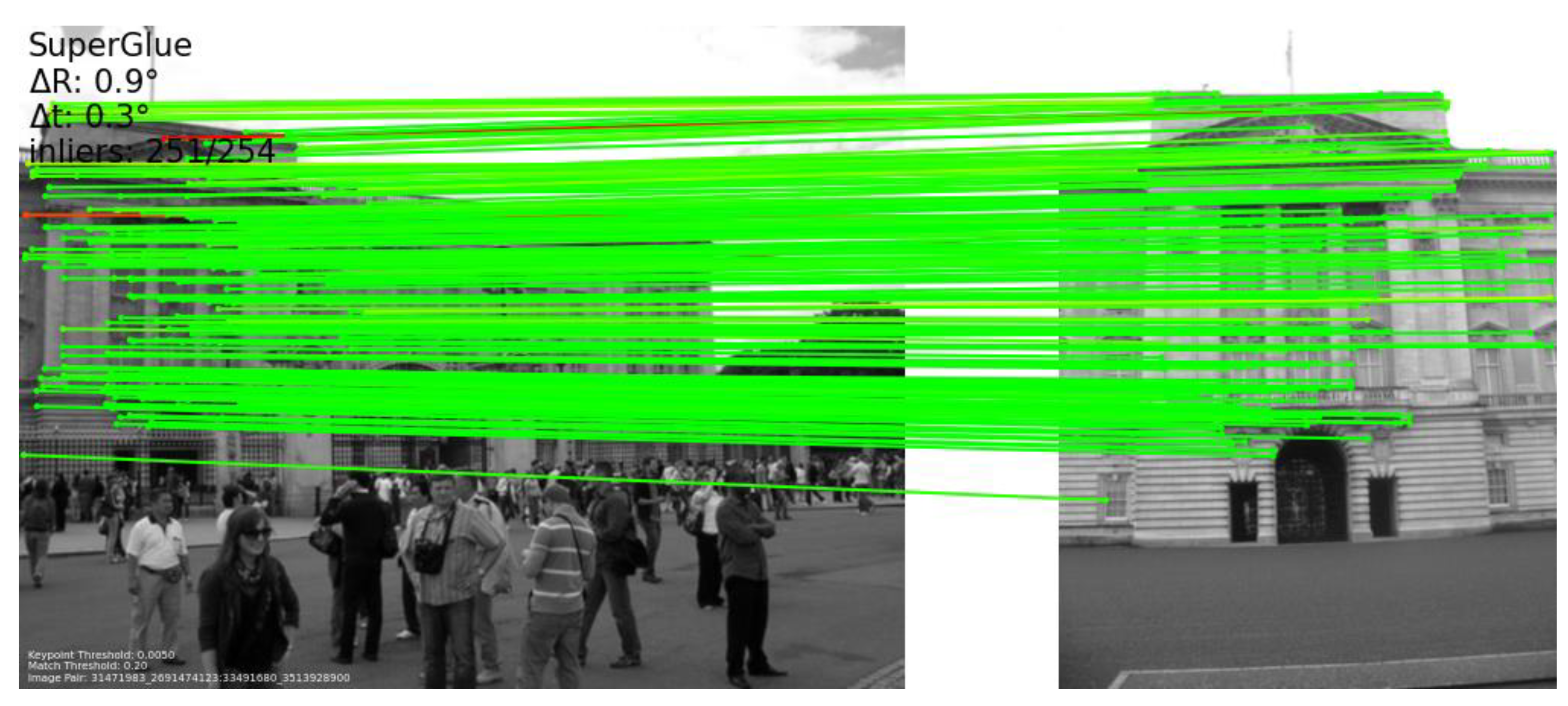
A total of 4000 pairs of images are tested on a trained SuperPoint neural network for matching. The matching score (M. Score) is the measure to determine the effectiveness of the matching technique. M. Score is the average ratio of the number of correct matches to the total number of detected keypoints. Figure 11 illustrates the visual results of extraction and matching of SuperPoint feature points. Initially, the feature points of both input images are extracted by the SuperPoint network. Then, the feature points of the two images are matched by the SuperGlue network [43]. Green pairs are the ones with an accurate matching, while red ones are mismatched. Then, the translation and rotation of the two images are estimated and compared with the ground truth. The error of estimation is very small, showing that SuperPoint has a high M. Score. Table 4 shows the matching results of the proposed technique using SuperPoint neural-network-based feature point extraction and SuperGlue for matching. The simulation results show a high M. Score as compared to the baseline of 32-bit floating-point architecture. Moreover, the M. Score of Figure 11 is 32.86, which is 1.4× better than floating-point results.

5.3. ReLU Optimization and Simulation

As discussed in Section 4, ReLU hardware optimization is implemented without storing intermediate results and partial sum to off-chip memory. ReLU activation function is a single-point operation and it is critical to optimize the data path for successful implementation of ReLU operation. There are only two clock cycles to generate a result of K × K window convolution. However, the partial sum is received at every clock cycle and we need two pipeline registers to manage the ReLU calculation, as shown in Figure 9. The simulation results are depicted in Figure 12. It can be observed that on the first clock cycle, the data are fetched from on-chip memory, addition is performed with incoming data from each PE unit, and new sum data are written back to the memory at the second clock cycle.

5.4. Area and Power of PE unit

The PE unit of previous work [26] is synthesized using Synopsys design compiler (DC), and the results are compared with our proposed design, as presented in Table 5. Both architectures use the parallelism of FP and SP; therefore, each PE unit takes ( K × T M ) pair of input features and weights at each clock cycle. To compare the PE design with previous work, the design of the PE unit in [26] is modified to make a fair comparison with this design in terms of area, power, and speed. Table 5 shows that both designs implement the same number of operations. There is an area reduction of 1.5×, and 1.2× improvement in terms of power consumption of this work. The design in [26] does not use built-in adders and multipliers; instead, Booth-encoding multipliers with Wallace tree adders for its PE design are implemented.

5.5. Input Image and Weight Memories

Figure 13 shows memory utilization compared with the traditional ping-pong memory technique. Figure 13a represents the percentage improvement of active memory locations for each convolution layer group. It can be observed that a maximum of 67% improvement in memory utilization is achieved, as compared to a traditional approach. Figure 13b shows the overall memory utilization for implemented SuperPoint architecture. For the input image, there is a considerable improvement of 50% in memory size as compared to a traditional approach, and an overall 35% of memory size is reduced. Therefore, it shows the effectiveness of the proposed design technique that is implemented in this work.
Figure 13. On-chip memory size comparison. (a) The results are for traditional ping-pong memory technique with proposed design. (b) The overall memory size comparison.
Electronics 11 04168 g013aElectronics 11 04168 g013b

5.6. Reusability of Data

The SuperPoint neural network size is very large (∼46 GOPS) and it requires a large amount of data movement from off-chip to on-chip. Therefore, as discussed in Section 4, the architecture is designed to fully utilize the intermediate and partial sums generated in a process of convolution without moving data to off-chip memories. As a result, it reduces off-chip data transactions and power consumption. The architecture is also pipelined, and after initial latency, the results are generated at every clock cycle. ReLU architecture is designed to manage the one-point computation of the ReLU activation function. Moreover, memory organization is arranged to manage the overlapping of data.
The architecture also exploits the loop unrolling and tiling. It uses the FP and SP parallelism that further relaxes the architecture to work in parallel on input feature maps and generate output features at the same time. Further, it can be observed from Figure 13 that a considerable amount of memory is saved.

5.7. Implementation Results and Comparison

5.7.1. Overall Chip Area and Power Consumption

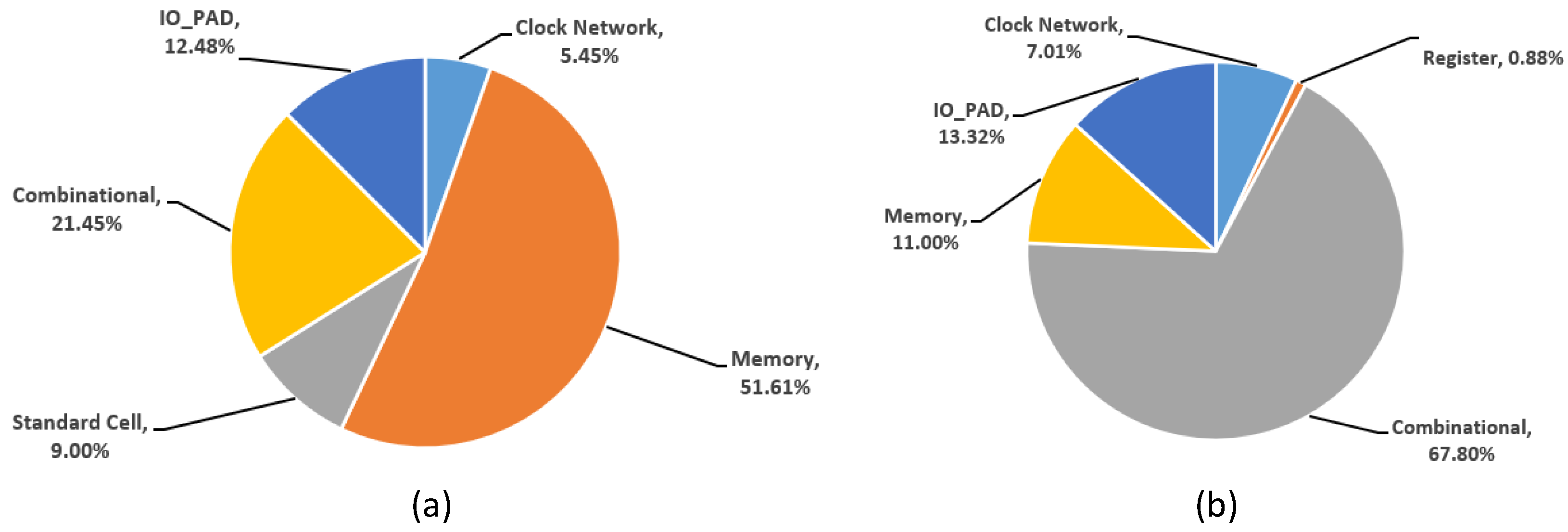
Figure 10 shows the chip picture, and its core area is 3.3 × 2.5 mm2. In simulation, the chip consumes power of 203 mW with a core voltage of 1.2 V. The total number of PEs is 16 and the number of operations is 816. Figure 14 shows the chip area and simulated component-wise power breakdown. The power breakdown is obtained through the post-layout simulation with actual workloads. The area breakdown is obtained using the area report of post-place and route. The power consumption of memories remains at 11% and the area occupied by memories is 51.61%. This is because a multi-bank memory system is employed using FP and SP to support the proposed data path.

5.7.2. Comparison with other ASIC designs

FPSNET achieves a peak throughput of 204 GOPS at a working frequency of 250 MHz. The power efficiency of 1.0 TOPS/W is achieved by the FPSNET for SuperPoint architecture.
To the best of our knowledge, this is the first ASIC design for SLAM application for feature point extraction using a SuperPoint neural network. However, to make a comparison, we compared the FPSNET accelerator chip with the previous ASIC designs, which are proposed as general-purpose accelerators. Table 6 shows the comparison of FPSNET with other neural network architectures.
FPSNET architecture is based on 16-bit fixed-point architecture, while other architectures use a different number of precision bits. We tried to make a comparison for other designs using a 16-bit design and with the same technology of 65 nm. The power efficiency results without voltage scaling are reported and compared with FPSNET. Eyeriss achieved a peak throughput of 84 GOPS with a power efficiency of 0.14 TOPS/W at 16 bits. However, FPSNET performed 2.4× better in terms of throughput and 7.1× better considering power efficiency as compared to Eyeriss. Moreover, DNPU [44] performed 1.5× better in terms of throughput than FPSNET but it has the same power efficiency. ENVISION [45] and THINKER [32] can operate on 4, 8, and 16 bits with peak throughput of 76 @ 4b and 410 @ 8b GOPS, respectively. It can be observed that the FPSNET achieved a 2× improvement in performance with the state-of-the-art design STICKER [32]. Moreover, it also achieved a power efficiency of 1.0 TOPS/W, which is 2.4× improved efficiency, as compared to STICKER. Considering the efficiency concerning area, FPSNET has 1.9× better area efficiency compared to STICKER. As FPSNET is compared with other designs using the same technology of 65 nm, compared to the DNPU [44] and THINKER [21] with close peak throughput and power efficiency performance, the presented FPSNET has the smallest chip area (at least 42.4% reduction).

6. Conclusions

The FPSNET architecture is proposed and designed in 65 nm CMOS technology for the feature point extraction in SLAM using SuperPoint neural network. The proposed chip consists of 16 PE units that can achieve a peak throughput of 204 GOPS at a working frequency of 250 MHz. To improve the power efficiency, data path optimization is deployed, which reduces the off-chip memory access operations. FPSNET avoids data overlapping to on-chip memories with specially designed address generation logic. Moreover, the optimized ReLU hardware technique is implemented without transferring the partial sum to off-chip memory. With all these optimization techniques, the presented FPSNET achieved remarkable chip area and power efficiency improvement compared to other ASIC designs in the literature.

Author Contributions

Conceptualization, F.U.D.F.; data curation, W.Z.; formal analysis, C.Z.; funding acquisition, C.Z. and Z.W.; investigation, F.U.D.F.; methodology, F.U.D.F.; project administration, C.Z., Z.W., and H.J.; resources, Z.W.; software, W.Z.; supervision, C.Z.; validation, F.U.D.F.; visualization, F.U.D.F.; writing—original draft, F.U.D.F.; writing—review and editing, Weiyi Zhang and Hanjun Jiang. All authors have read and agreed to the published version of the manuscript.

Funding

This work was supported by the National Natural Science Foundation of China (No. U20A20220).

Data Availability Statement

The datasets analyzed during the current study are available from the corresponding author upon reasonable request.

Conflicts of Interest

The authors declare that they have no competing financial or nonfinancial interests.

References

  1. Gao, X.; Zhang, T. Introduction to Visual SLAM: From Theory to Practice; Springer Nature: Singapore, 2021. [Google Scholar]
  2. Chen, W.; Shang, G.; Ji, A.; Zhou, C.; Wang, X.; Xu, C.; Li, Z.; Hu, K. An Overview on Visual SLAM: From Tradition to Semantic. Remote. Sens. 2022, 14, 3010. [Google Scholar] [CrossRef]
  3. Li, D.; Shi, X.; Long, Q.; Liu, S.; Yang, W.; Wang, F.; Wei, Q.; Qiao, F. DXSLAM: A Robust and Efficient Visual SLAM System with Deep Features. arXiv 2020, arXiv:2008.05416. [Google Scholar]
  4. Bay, H.; Tuytelaars, T.; Van Gool, L. SURF: Speeded Up Robust Features. In Proceedings of the Computer Vision—ECCV 2006, Graz, Austria, 7–13 May 2006; Leonardis, A., Bischof, H., Pinz, A., Eds.; Springer: Berlin/Heidelberg, Germany, 2006; pp. 404–417. [Google Scholar]
  5. Rublee, E.; Rabaud, V.; Konolige, K.; Bradski, G. ORB: An efficient alternative to SIFT or SURF. In Proceedings of the 2011 International Conference on Computer Vision, Barcelona, Spain, 6–13 November 2011; pp. 2564–2571. [Google Scholar] [CrossRef]
  6. Lowe, D. Object recognition from local scale-invariant features. In Proceedings of the Seventh IEEE International Conference on Computer Vision, Corfu, Greece, 20–27 September 1999; Volume 2, pp. 1150–1157. [Google Scholar] [CrossRef]
  7. DeTone, D.; Malisiewicz, T.; Rabinovich, A. SuperPoint: Self-Supervised Interest Point Detection and Description. In Proceedings of the 2018 IEEE/CVF Conference on Computer Vision and Pattern Recognition Workshops (CVPRW), Salt Lake City, UT, USA, 18–22 June 2018; pp. 337–33712. [Google Scholar] [CrossRef] [Green Version]
  8. Simo-Serra, E.; Trulls, E.; Ferraz, L.; Kokkinos, I.; Fua, P.; Moreno-Noguer, F. Discriminative Learning of Deep Convolutional Feature Point Descriptors. In Proceedings of the 2015 IEEE International Conference on Computer Vision (ICCV), Santiago, Chile, 7–13 December 2015; pp. 118–126. [Google Scholar] [CrossRef] [Green Version]
  9. Radenović, F.; Tolias, G.; Chum, O. Fine-Tuning CNN Image Retrieval with No Human Annotation. IEEE Trans. Pattern Anal. Mach. Intell. 2019, 41, 1655–1668. [Google Scholar] [CrossRef] [PubMed] [Green Version]
  10. Zhang, W.; Jiang, Y.; Din Farrukh, F.U.; Zhang, C.; Xie, X. A Portable Accelerator of Proximal Policy Optimization for Robots. In Proceedings of the 2021 IEEE International Conference on Integrated Circuits, Technologies and Applications (ICTA), Zhuhai, China, 24–26 November 2021; pp. 171–172. [Google Scholar] [CrossRef]
  11. Dong, P.; Li, Z.; Chen, Z.; Yao, R.; Deng, H.; Zhang, W.; Zhang, Y.; Chen, L.; Wang, C.; An, F. A 139 fps pixel-level pipelined binocular stereo vision accelerator with region-optimized semi-global matching. In Proceedings of the 2021 IEEE Asian Solid-State Circuits Conference (A-SSCC), Busan, Korea, 7–10 November 2021; pp. 1–3. [Google Scholar] [CrossRef]
  12. Yu, J.; Xu, Z.; Zeng, S.; Yu, C.; Qiu, J.; Shen, C.; Xu, Y.; Dai, G.; Wang, Y.; Yang, H. INCA: INterruptible CNN Accelerator for Multi-tasking in Embedded Robots. In Proceedings of the 2020 57th ACM/IEEE Design Automation Conference (DAC), San Francisco, CA, USA, 20–24 July 2020; pp. 1–6. [Google Scholar] [CrossRef]
  13. Xu, Z.; Yu, J.; Yu, C.; Shen, H.; Wang, Y.; Yang, H. CNN-based Feature-point Extraction for Real-time Visual SLAM on Embedded FPGA. In Proceedings of the 2020 IEEE 28th Annual International Symposium on Field-Programmable Custom Computing Machines (FCCM), Fayetteville, AR, USA, 3–6 May 2020; pp. 33–37. [Google Scholar] [CrossRef]
  14. Liu, Y.; Li, J.; Huang, K.; Li, X.; Qi, X.; Chang, L.; Long, Y.; Zhou, J. MobileSP: An FPGA-Based Real-Time Keypoint Extraction Hardware Accelerator for Mobile VSLAM. IEEE Trans. Circuits Syst. I Regul. Pap. 2022, 69, 3190300. [Google Scholar] [CrossRef]
  15. Sun, H.; Deng, Q.; Liu, X.; Shu, Y.; Ha, Y. An Energy-Efficient Stream-Based FPGA Implementation of Feature Extraction Algorithm for LiDAR Point Clouds With Effective Local-Search. IEEE Trans. Circuits Syst. I Regul. Pap. 2022, 3212075. [Google Scholar] [CrossRef]
  16. Parashar, A.; Rhu, M.; Mukkara, A.; Puglielli, A.; Venkatesan, R.; Khailany, B.; Emer, J.; Keckler, S.W.; Dally, W.J. SCNN: An accelerator for compressed-sparse convolutional neural networks. In Proceedings of the 2017 ACM/IEEE 44th Annual International Symposium on Computer Architecture (ISCA), Toronto, ON, Canada, 24–28 June 2017; pp. 27–40. [Google Scholar] [CrossRef]
  17. Li, J.; Jiang, S.; Gong, S.; Wu, J.; Yan, J.; Yan, G.; Li, X. SqueezeFlow: A Sparse CNN Accelerator Exploiting Concise Convolution Rules. IEEE Trans. Comput. 2019, 68, 1663–1677. [Google Scholar] [CrossRef]
  18. Lee, J.; Kim, C.; Kang, S.; Shin, D.; Kim, S.; Yoo, H.J. UNPU: An Energy-Efficient Deep Neural Network Accelerator With Fully Variable Weight Bit Precision. IEEE J. Solid-State Circuits 2019, 54, 173–185. [Google Scholar] [CrossRef]
  19. Lu, W.; Yan, G.; Li, J.; Gong, S.; Han, Y.; Li, X. FlexFlow: A Flexible Dataflow Accelerator Architecture for Convolutional Neural Networks. In Proceedings of the 2017 IEEE International Symposium on High Performance Computer Architecture (HPCA), Austin, TX, USA, 4–8 February 2017; pp. 553–564. [Google Scholar] [CrossRef]
  20. Shin, D.; Lee, J.; Lee, J.; Lee, J.; Yoo, H.J. DNPU: An Energy-Efficient Deep-Learning Processor with Heterogeneous Multi-Core Architecture. IEEE Micro 2018, 38, 85–93. [Google Scholar] [CrossRef]
  21. Yin, S.; Ouyang, P.; Tang, S.; Tu, F.; Li, X.; Zheng, S.; Lu, T.; Gu, J.; Liu, L.; Wei, S. A High Energy Efficient Reconfigurable Hybrid Neural Network Processor for Deep Learning Applications. IEEE J. Solid-State Circuits 2018, 53, 968–982. [Google Scholar] [CrossRef]
  22. Chen, Y.H.; Yang, T.J.; Emer, J.; Sze, V. Eyeriss v2: A Flexible Accelerator for Emerging Deep Neural Networks on Mobile Devices. IEEE J. Emerg. Sel. Top. Circuits Syst. 2019, 9, 292–308. [Google Scholar] [CrossRef] [Green Version]
  23. Nguyen, D.T.; Nguyen, T.N.; Kim, H.; Lee, H.J. A High-Throughput and Power-Efficient FPGA Implementation of YOLO CNN for Object Detection. IEEE Trans. Very Large Scale Integr. (Vlsi) Syst. 2019, 27, 1861–1873. [Google Scholar] [CrossRef]
  24. Zhang, C.; Li, P.; Sun, G.; Guan, Y.; Xiao, B.; Cong, J. Optimizing FPGA-based Accelerator Design for Deep Convolutional Neural Networks. In Proceedings of the 2015 ACM/SIGDA International Symposium on Field-Programmable Gate Arrays, Monterey, CA, USA, 22–24 February 2015. [Google Scholar]
  25. Sun, F.; Wang, C.; Gong, L.; Xu, C.; Zhang, Y.; Lu, Y.; Li, X.; Zhou, X. A High-Performance Accelerator for Large-Scale Convolutional Neural Networks. In Proceedings of the 2017 IEEE International Symposium on Parallel and Distributed Processing with Applications and 2017 IEEE International Conference on Ubiquitous Computing and Communications (ISPA/IUCC), Guangzhou, China, 12–15 December 2017; pp. 622–629. [Google Scholar] [CrossRef]
  26. Farrukh, F.U.D.; Zhang, C.; Jiang, Y.; Zhang, Z.; Wang, Z.; Wang, Z.; Jiang, H. Power Efficient Tiny Yolo CNN Using Reduced Hardware Resources Based on Booth Multiplier and WALLACE Tree Adders. IEEE Open J. Circuits Syst. 2020, 1, 76–87. [Google Scholar] [CrossRef]
  27. Li, H.; Fan, X.; Jiao, L.; Cao, W.; Zhou, X.; Wang, L. A high performance FPGA-based accelerator for large-scale convolutional neural networks. In Proceedings of the 2016 26th International Conference on Field Programmable Logic and Applications (FPL), Lausanne, Switzerland, 29 August–2 September 2016; pp. 1–9. [Google Scholar] [CrossRef]
  28. Jokic, P.; Emery, S.; Benini, L. Improving Memory Utilization in Convolutional Neural Network Accelerators. IEEE Embed. Syst. Lett. 2021, 13, 77–80. [Google Scholar] [CrossRef]
  29. Karl, E.; Wang, Y.; Ng, Y.G.; Guo, Z.; Hamzaoglu, F.; Meterelliyoz, M.; Keane, J.; Bhattacharya, U.; Zhang, K.; Mistry, K.; et al. A 4.6 GHz 162 Mb SRAM Design in 22 nm Tri-Gate CMOS Technology With Integrated Read and Write Assist Circuitry. IEEE J. Solid-State Circuits 2013, 48, 150–158. [Google Scholar] [CrossRef]
  30. Horowitz, M. 1.1 Computing’s energy problem (and what we can do about it). In Proceedings of the 2014 IEEE International Solid-State Circuits Conference Digest of Technical Papers (ISSCC), San Francisco, CA, USA, 9–13 February 2014; pp. 10–14. [Google Scholar] [CrossRef]
  31. Yang, X.S.; Pu, J.; Rister, B.; Bhagdikar, N.; Richardson, S.; Kvatinsky, S.; Ragan-Kelley, J.; Pedram, A.; Horowitz, M. A Systematic Approach to Blocking Convolutional Neural Networks. arXiv 2016, arXiv:1606.04209. [Google Scholar]
  32. Yuan, Z.; Liu, Y.; Yue, J.; Yang, Y.; Wang, J.; Feng, X.; Zhao, J.; Li, X.; Yang, H. STICKER: An Energy-Efficient Multi-Sparsity Compatible Accelerator for Convolutional Neural Networks in 65-nm CMOS. IEEE J. Solid-State Circuits 2020, 55, 465–477. [Google Scholar] [CrossRef]
  33. Mur-Artal, R.; Montiel, J.M.M.; Tardós, J.D. ORB-SLAM: A Versatile and Accurate Monocular SLAM System. IEEE Trans. Robot. 2015, 31, 1147–1163. [Google Scholar] [CrossRef] [Green Version]
  34. Engel, J.; Schöps, T.; Cremers, D. LSD-SLAM: Large-Scale Direct Monocular SLAM. In Proceedings of the Computer Vision—ECCV 2014, Zurich, Switzerland, 6–12 September 2014; Fleet, D., Pajdla, T., Schiele, B., Tuytelaars, T., Eds.; Springer International Publishing: Cham, Switzerland, 2014; pp. 834–849. [Google Scholar]
  35. Kang, R.; Shi, J.; Li, X.; Liu, Y.; Liu, X. DF-SLAM: A Deep-Learning Enhanced Visual SLAM System based on Deep Local Features. arXiv 2019, arXiv:1901.07223. [Google Scholar] [CrossRef]
  36. Simonyan, K.; Zisserman, A. Very Deep Convolutional Networks for Large-Scale Image Recognition. arXiv 2014, arXiv:1901.07223. [Google Scholar] [CrossRef]
  37. Qiu, J.; Wang, J.; Yao, S.; Guo, K.; Li, B.; Zhou, E.; Yu, J.; Tang, T.; Xu, N.; Song, S.; et al. Going Deeper with Embedded FPGA Platform for Convolutional Neural Network. In Proceedings of the 2016 ACM/SIGDA International Symposium on Field-Programmable Gate Arrays, Association for Computing Machinery (FPGA ’16), New York, NY, USA, 21–23 February 2016; pp. 26–35. [Google Scholar] [CrossRef]
  38. Shen, Y.; Ferdman, M.; Milder, P. Maximizing CNN Accelerator Efficiency Through Resource Partitioning. In Proceedings of the 44th Annual International Symposium on Computer Architecture, Association for Computing Machinery (ISCA ’17), New York, NY, USA, 24–28 June 2017; pp. 535–547. [Google Scholar] [CrossRef] [Green Version]
  39. Lu, L.; Liang, Y.; Xiao, Q.; Yan, S. Evaluating Fast Algorithms for Convolutional Neural Networks on FPGAs. In Proceedings of the 2017 IEEE 25th Annual International Symposium on Field-Programmable Custom Computing Machines (FCCM), Napa, CA, USA, 30 April–2 May 2017; pp. 101–108. [Google Scholar] [CrossRef]
  40. Liang, S.; Yin, S.; Liu, L.; Luk, W.; Wei, S. FP-BNN: Binarized neural network on FPGA. Neurocomputing 2018, 275, 1072–1086. [Google Scholar] [CrossRef]
  41. Chen, Y.H.; Krishna, T.; Emer, J.S.; Sze, V. Eyeriss: An Energy-Efficient Reconfigurable Accelerator for Deep Convolutional Neural Networks. IEEE J. Solid-State Circuits 2017, 52, 127–138. [Google Scholar] [CrossRef] [Green Version]
  42. Lin, T.; Maire, M.; Belongie, S.J.; Bourdev, L.D.; Girshick, R.B.; Hays, J.; Perona, P.; Ramanan, D.; Dollár, P.; Zitnick, C.L. Microsoft COCO: Common Objects in Context. arXiv 2014, arXiv:1405.0312. [Google Scholar]
  43. Sarlin, P.E.; DeTone, D.; Malisiewicz, T.; Rabinovich, A. SuperGlue: Learning Feature Matching With Graph Neural Networks. In Proceedings of the 2020 IEEE/CVF Conference on Computer Vision and Pattern Recognition (CVPR), Seattle, WA, USA, 13–19 June 2020; pp. 4937–4946. [Google Scholar] [CrossRef]
  44. Shin, D.; Lee, J.; Lee, J.; Yoo, H.J. 14.2 DNPU: An 8.1TOPS/W reconfigurable CNN-RNN processor for general-purpose deep neural networks. In Proceedings of the 2017 IEEE International Solid-State Circuits Conference (ISSCC), San Francisco, CA, USA, 5–9 February 2017; pp. 240–241. [Google Scholar] [CrossRef]
  45. Moons, B.; Uytterhoeven, R.; Dehaene, W.; Verhelst, M. 14.5 Envision: A 0.26-to-10TOPS/W subword-parallel dynamic-voltage-accuracy-frequency-scalable Convolutional Neural Network processor in 28 nm FDSOI. In Proceedings of the 2017 IEEE International Solid-State Circuits Conference (ISSCC), San Francisco, CA, USA, 19–23 February 2017; pp. 246–247. [Google Scholar] [CrossRef]
Figure 1. SuperPoint-based feature point extraction.
Electronics 11 04168 g001
Figure 2. SuperPoint network model.
Electronics 11 04168 g002
Figure 3. Loop unrolling and parallel architecture.
Electronics 11 04168 g003
Figure 4. Streaming convolution layer data flow.
Electronics 11 04168 g004
Figure 5. Architecture overview.
Electronics 11 04168 g005
Figure 7. Conv1b layer example for data arrangement. (a) Input image data; (b) input weights data.
Electronics 11 04168 g007
Figure 8. Proposed data arrangement technique.
Electronics 11 04168 g008
Figure 9. Proposed ReLU processing design. The AGU generates the required read/write address and SC produces the required control signals. (a) Interconnection between PEs and ReLU design in the output module. (b) Initially, a normal partial sum writes to output memories. (c) For the next partial sum, logic is implemented for reading, the addition of results, and writing back data to memories.
Electronics 11 04168 g009
Figure 10. ASIC layout and specifications.
Electronics 11 04168 g010
Figure 11. Simulation results of feature points extraction and matching.
Electronics 11 04168 g011
Figure 12. Simulation of ReLU hardware design.
Electronics 11 04168 g012
Figure 14. (a) Area breakdown. (b) Component-wise power breakdown.
Electronics 11 04168 g014
Table 1. Configuration word information.
Signal NameRegister Bit(s)Information
Conv 1 C [ 0 ] Convolution start command
SpL C [ 1 ] Special command for 1st Conv1a input feature
L N o C [ 3 : 2 ] Convolution layer group number
I t r N o C [ 5 : 4 ] Iteration number for input features ( I t r N o = F I N / ( F c × T M ) )
F c C [ 10 : 6 ] Stored number of input features in each memory
ConvP C [ 11 ] Convolution done pulse
1 C: 64-bit control register.
Table 2. Address decoding.
Mode1 A [ 20 : 18 ] A [ 17 : 14 ] A [ 13 : 11 ]
Image Mem. WR 2001xxxx000-111
Weights Mem. WR0100000-1111000-111
Output Mem. RD 3011xxxx000-011
Control Reg. WR100xxxxxxx
Status Reg. RD101xxxxxxx
1A: 21-bit address bus. 2 WR: write. 3 RD: read.
Table 3. Convolution layer parameters for input image and weights.
Conv. Layer No. F IN F OUT H in    W in      P      F c       I mem    Itr No W mem
Conv1a164480640True16421 124
Conv1b6464480640True21284424
Conv2a6464240320True41288224
Conv2b6464240320True41288224
Conv3a64128120160True81296148
Conv3b128128120160True81296248
Conv4a1281286080True161312148
Conv4b1281286080True161312148
1ItrNo = 1: Special case for 1st Conv1a layer.
Table 4. Matching results.
Quantization1 AUC@5AUC@10AUC@20PrecisionM. Score
Baseline (32-bit floating point)39.5059.7475.9598.6723.85
Our work (16-bit fixed point)36.7656.8473.4698.5433.85
1 AUC: area under the cumulative error curve.
Table 5. Comparison of PE unit.
MetricsOJCAS [26]This Work
Precision (bit)1616
Technology (nm)6565
Area (mm2)0.07390.0494
Frequency (MHz)250300
No. of operations4848
No. of MACs2424
Power (mW)8.7257.115
Table 6. Comparison with previous ASIC designs.
Eyeriss ISSCC2016 [41]DNPU ISSCC2017 [44]ENVISION ISSCC2017 [45]THINKER JSSC18 [21]STICKER JSSC19 [32]Our Work (FPSNET)
Technology (nm)656528656565
Core Area (mm2)12.316.01.914.47.88.3
Voltage (V)1.171.11.11.21.01.2
On-chip SRAM (kB)181.5290144348170176
Core Frequency (MHz)200200200200200250
Number of PEs16877625651225616
Number of MACs1687685121024256384
Peak Performance (TOPS)0.084 @ 16b0.300 @ 16b0.076 @ 4b0.410 @ 8b0.102 @ 8b0.204 @ 16b
Bit-width (bits)164/8/164/8/168/16816
Power (mW)450279300386248203
Power Efficiency (TOPS/W)0.141.00.261.060.4111.0
Efficiency w.r.t. Area (GOPS/mm2)6.8318.7540.028.4713.0824.73
Publisher’s Note: MDPI stays neutral with regard to jurisdictional claims in published maps and institutional affiliations.