Article

Circuit Modelling of Broadband Antenna Using Vector Fitting and Foster Form Approaches for IoT Applications

by
Fatima Ez-zaki
1,
Khaoula Ait Belaid
1,
Sarosh Ahmad
2,*,
Hassan Belahrach
1,3,
Abdelilah Ghammaz
1,
Ahmed Jamal Abdullah Al-Gburi
4 and
Naser Ojaroudi Parchin
5,*
1
Laboratory of Electrical Systems and Telecommunications, Faculty of Sciences and Technologies, Cadi Ayyad University, Avenue Abdelkarim Elkhattabi, P.O. Box 549, Marrakesh 40000, Morocco
2
Department of Signal Theory and Communications, Universidad Carlos III de Madrid (UC3M), Leganes, 28911 Madrid, Spain
3
Electrical Engineering Department, Royal School of Aeronautics, Marrakesh 40150, Morocco
4
Department of Electronics and Computer Engineering (FKEKK), Center for Telecommunication Research and Innovation (CeTRI), Universiti Teknikal Malaysia Melaka (UTeM), Durian Tungal 76100, Malaysia
5
School of Engineering and the Built Environment, Edinburgh Napier University, Edinburgh EH10 5DT, UK
*
Authors to whom correspondence should be addressed.
Electronics 2022, 11(22), 3724; https://doi.org/10.3390/electronics11223724
Submission received: 18 October 2022 / Revised: 9 November 2022 / Accepted: 11 November 2022 / Published: 14 November 2022
(This article belongs to the Special Issue Broadband Antennas and Antenna Arrays)

Abstract

:
Computation of the broadband antenna impedance behavior requires the wideband lumped equivalent circuit. This work aims to provide a comprehensive study of broadband antenna equivalent circuit models over broad frequency ranges for Internet of Things (IoT) applications using multiple approaches. The first approach is a Foster approximation, which is based on the antenna-simulated scattering parameters and impedance data. The second concerns a vector-fitting fitting approximation, which is based on the antenna-simulated impedance/admittance data. The studied antenna is modeled based on the radiating element’s geometry and the multifractal slots, in addition to the DGS (Defected Ground Plane) effects. Applying these techniques, wideband lumped equivalent circuits of the antenna have been computed which are in good agreement with measurement data. These models could be useful for the enhancement of the performance of a broadband antenna and its systematic design as well as offering the advantage of saving computation time for full-wave simulations and facilitating the solution of problems that have both an electromagnetic part as well as a circuit part. For further analysis, the Gaussian pulse has been generated to drive a time-domain analysis of the current and power response waveforms antenna behavior under load.

1. Introduction

Rapid development in wireless communications has resulted in a rising need for small antennas that can function across many frequency bands to meet the requirements of various applications. Therefore, it is preferred to have a single integrated antenna structure that can operate across a wide range of frequencies while keeping the system’s footprint as small as possible. For this reason, antenna designs that combine the capabilities of several antennas into a single emitter structure have surged in popularity in recent years. On the other hand, multiband antennas reduce electromagnetic interference and pulse distortion effects. Moreover, their desirable characteristics, such as integration ease, lightweight, compact size, and low manufacturing cost, make them the preferred choice over their counterparts and excellent choices for modern wireless communication systems.
To further understanding of the antenna performance, it is recommended to obtain its equivalent circuit model. Such an electrical model can be very useful for circuit simulations, as might be desired in the analysis of an integrated antenna. Accordingly, the development of the electrical circuit model is important for its time-domain analysis, to understand the antenna resonance and structure, to derive mathematical equations, and to design a systematic antenna exploring the equivalent circuit [1,2,3,4,5,6,7,8,9,10,11,12,13]. Moreover, it helps predict the effects of integrating the antenna [11]. However, developing equivalent circuits for complicated antenna configurations that have numerous resonances is a difficult task [13].
To design antenna structures, rigorous numerical methods are employed to resolve electromagnetic equations in integral or differential forms, such as CST, HFSS and FEKO, are employed. The concern is that these methods offer better accuracy, but they have some limitations [4,6,9]. They cannot cover all kinds of losses. Moreover, they generally require a long and cumbersome computation with complicated settings and cost consumption. Moreover, the equivalent circuit model, either in the form of a transmission line model or in the form of a lumped circuit model of antennas is widely used to enhance the antenna design features by considering antennas as load impedances.
The lumped equivalent circuit parameters can be computed either from the curve fitting method, using the rational approximation of frequency responses of the antenna, based on the cavity model of the antenna, or from graphical methods. A previous study reported in [4] that an RFID antenna was modelled as a parallel RLC circuit. The geometric dimensions of the antenna and the dielectric properties were used to determine the RLC parameters. In [13], we see that the rational approximation of the frequency domain response of a dual-band Planer Inverted-F Antenna (PIFA) and its lumped equivalent circuit formulation may be used to improve their performance. The UHF small double E-shaped meander line printed monopole antenna circuit model was produced by the authors of reference [14] using inductance and capacitance circuits. All of the circuits were linked in parallel. Using the work provided in [15], it is possible to demonstrate that the equivalent circuit model of a small multi-band antenna may be built using a series of parallel RLC circuits. Thus, the input impedance curve is used as a starting point for the initial values of the RLC parameters. Furthermore, in [16], researchers provide a novel method for determining the wideband lumped equivalent circuit of rectangular and E-shaped microstrip antennas. By using a nonlinear curve-fitting optimization strategy, the starting values for the equivalent circuit parameters are derived. With [17,18], a method is provided for generating wideband electrical models of frequency-domain responses approximating rational functions, which may be used in SPICE. They have shown that low-rank approximations of one-port or two-port systems may be effectively generated using the fitting method or reduced-order models. An alternative approach to the circuit modeling problem of the broadband antenna using frequency domain data from simulations or measurements was introduced in [19]. Using this method, an equivalent circuit may be created for use with broadband antennas, which is an intriguing prospect. An approach is also provided for establishing the antenna’s input impedance model in the frequency domain, which involves the generation of a rational function approximation with actual coefficients. Several circuit models have been made to perform equivalent-circuit models of different UWB antenna shapes [20,21,22,23,24]. Some available and helpful equivalent circuit model synthesizing techniques were discussed and reported in [17,25,26,27,28,29,30,31,32,33,34,35,36,37,38,39,40] for readers’ further and deep knowledge.
The aim of this work is to review the most important circuit synthesis approaches to derive lumped equivalent circuits for a broadband antenna based on frequency domain S-parameters/Admittance/impedance data. The lumped equivalent circuit of the designed antenna is derived from the rational approximation of its frequency domain response using Foster approximation, the vector-fitting approach (VF), and based on antenna geometry and substrate characteristics. Subsequently, the derived equivalent circuits are simulated in Advanced Design System (ADS) software. The accuracy of the models has been validated by comparing its transient response with the antenna measurement result. Afterward, the model’s transient response is driven, and a time-domain analysis is performed to study the voltage, current, and power response waveforms of the antenna equivalent circuit. The generated models can then be connected to linear or nonlinear devices or localized elements to analyze the electromagnetic problems in the circuits associated with the antenna. The model can be used for any SPICE-based simulator tools; hence, it can be used in the co-design of the transmitter and receiver in circuit simulators.
The following is the outline for this paper: Foster approximation and rational function approximation using a vector-fitting method are two examples of the methods that are examined here. The equivalent circuit models of broadband antennas are calculated using the aforementioned methods, and their simulation results are shown in Section 2. In Section 3, we conduct a thorough time-domain analysis in ADS software of the antenna equivalent circuit with a pulse produced from the seventh Gaussian derivative. Section 4 provides some last thoughts on the matter.

2. Broadband Antenna Equivalent Circuit Methodologies

The antenna in Figure 1a was adopted to obtain further in-depth information on how the previously discussed approaches can be applied.

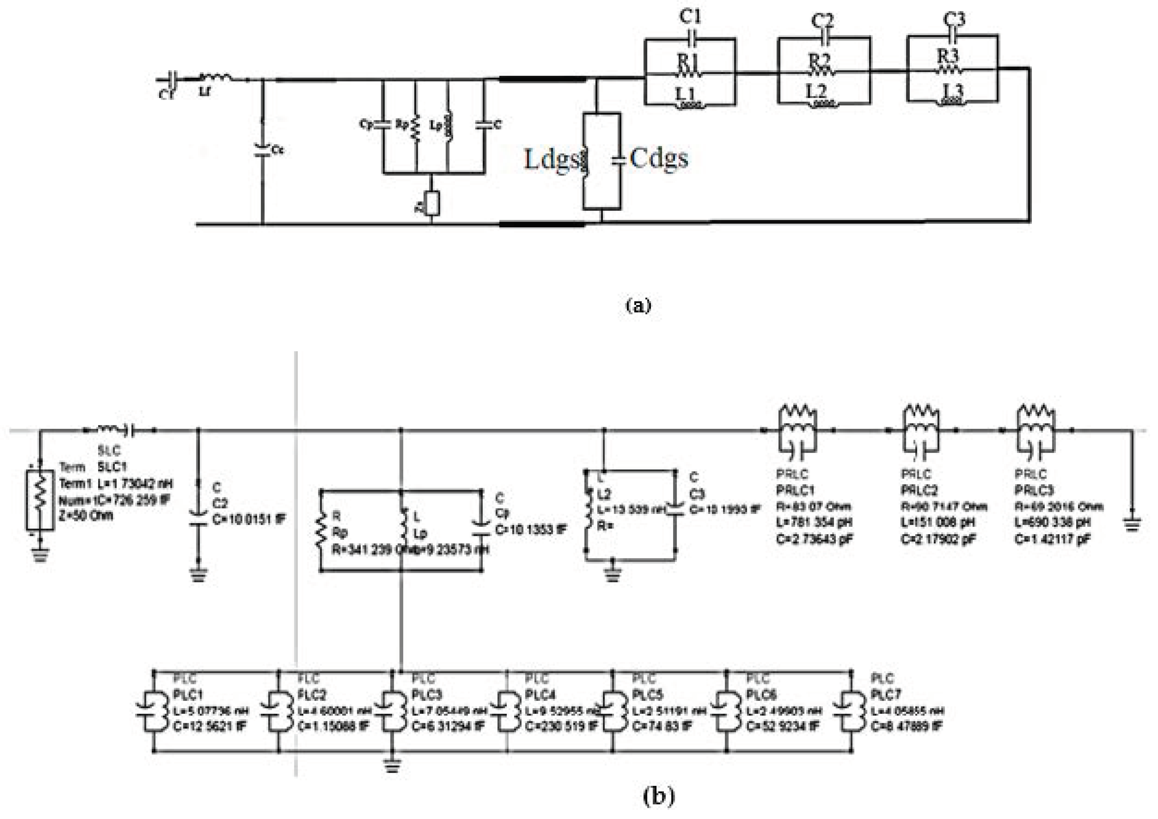
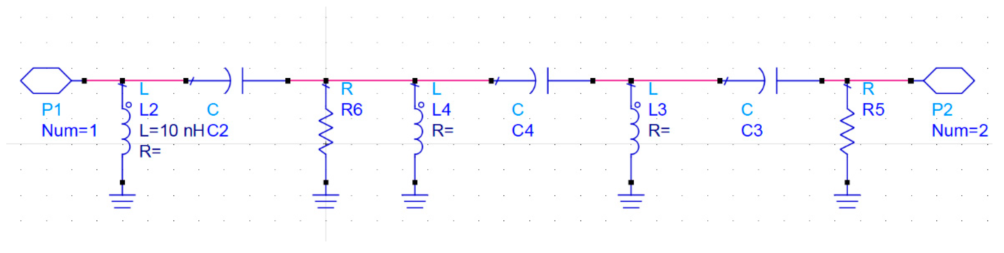
2.1. Stage I: Equivalent Circuit Model via Foster Canonical Form

Based on First Foster approximation, the input impedance Zin of an antenna is represented by the following Equation (1):
Z i n ( ω ) j ω L 0 + 1 j ω C 0 + n = 1 N m a x R n 1 + j Q n ( ω ω n ω n ω )
where Nmax is the number of modes required to accurately describe the frequency behavior of the antenna input impedance, Qn = ω nRnCn and   ω n = (LnCn)−0.5. is the operating angular frequency, and ω n is the resonant angular frequency of the nth resonant mode. C0 is the quasi-static input capacitance, and L0 is an inductance that accounts for higher-order modes as well as for feed effects, while Cn, Ln, Rn, and Qn are the capacitance, inductance, resistance, and quality factor, respectively, describing the antenna’s resonant processes [4,10].
The behavior of higher-order modes and antenna feed effects are modeled by C0 and L0 [38]. The quasi-static inductance L0 is generally infinitesimal when the order of the resonant modes is low. In particular, each mode is assumed to be characterized by a natural resonance ωn, a quality factor Qn, and a damping resistance Rn.
The capacitance C0 using Equation (2) [3,6].
C 0 = lim ω 0 + I m { Y i n E M ( ω ) } ω = lim ω 0 + I m { Y i n E M ( ω ) } ω I m { Y i n E M ( ω ) } ω
EM: CST MWS electromagnetic simulations.
where
ω = 2 π f   Y i n E M = 1 / Z i n E M
Furthermore, the resonant frequencies of the RLC dipoles can be calculated as a first approximation by determining the values ωn(0) for which the real part of Z i n E M has local maxima. Thus, the initial estimates of Rn and Qn are computed using Equations (3) and (4) [3,6]:
R n ( 0 ) = R e { Z i n E M ( ω n ( 0 ) ) }
Q n ( 0 ) = ω n ( 0 ) 2 R n ( 0 ) I m { Z i n E M ( ω n ( 0 ) ) } ω   ω n ( 0 ) I m { Z i n E M ( ω n ( 0 ) ω ) } I m { Z i n E M ( ω n ( 0 ) + ω ) } 4 R n ( 0 ) ω
Therefore, the values of L n ( 0 ) and C n ( 0 ) result from their mutual relations, namely given by Equation (5):
L n ( 0 ) = ( R n ( 0 ) Q n ( 0 ) ) C n ( 0 ) = R n ( 0 ) ω n ( 0 ) Q n ( 0 )
Therefore, it is easy to show that the quasi-static inductance can be estimated as follows (Equation (6)):
L 0 = 1 ( ω 0 ( 0 ) ) 2 C 0
where ω 0 ( 0 ) is the lower frequency for which I m { Z i n E M ( ω 0 ( 0 ) ) } = 0.
Figure 1b displays the results of CST simulations of the reflection coefficient (S11), while Figure 1c represents the real and imaginary sections of the input impedance curves of the examined antenna. An antenna’s equivalent circuit model may be derived from these curves, revealing its features at resonance. For example, in Figure 1b, each dip in the S11 curve might be interpreted as a different resonance frequency. The real and imaginary sections of the input impedance curve are about 50 and 0 Ohms, respectively, at these positions. That is to say, the factors considered are in agreement with resonant frequencies. Two such balance modes are found in the studied frequency range. As it turns out, a third-order circuit is presented as the basis for a lumped element model. Using resistors (Ri), inductors (Li), and capacitors (Ci), the suggested circuit model is a series of parallel RLC circuits. The actual component of the input impedance curve is used as a starting point for Ri (Equation (7)). The Formulas (8)–(11) are used to determine the starting values of the Li and Ci components.
R i = R e a l ( Z i n ( f r i ) )
Q i = f r i B W i = 2 π R i C i f r i
B W i = f h i f l i
C i = Q i 2 π f r i R i
L i = R i 2 C i Q i 2
In this expression, fri denotes the ith resonance frequency, Qi denotes the ith quality factor, fhi denotes the upper frequencies of the ith operating band, and fli denotes the lower frequencies of the ith operating band. When a monopole antenna is operating at its lower frequency, its capacitance, C0, and inductance, L0, should be selected such that the antenna resonates at its initial resonant frequency. The final values of the lumped circuit components are determined by tuning the circuit elements to obtain the desired response. In Figure 2 is shown the equivalent circuit that was calculated using the S11 data.
To check the validity of the established model, the ADS software was used. The circuit model frequency responses are compared with CST simulations. The results are depicted in Figure 3a,b. Based on these results, it is seen that both graphs agree well with each other with a slight shifting.

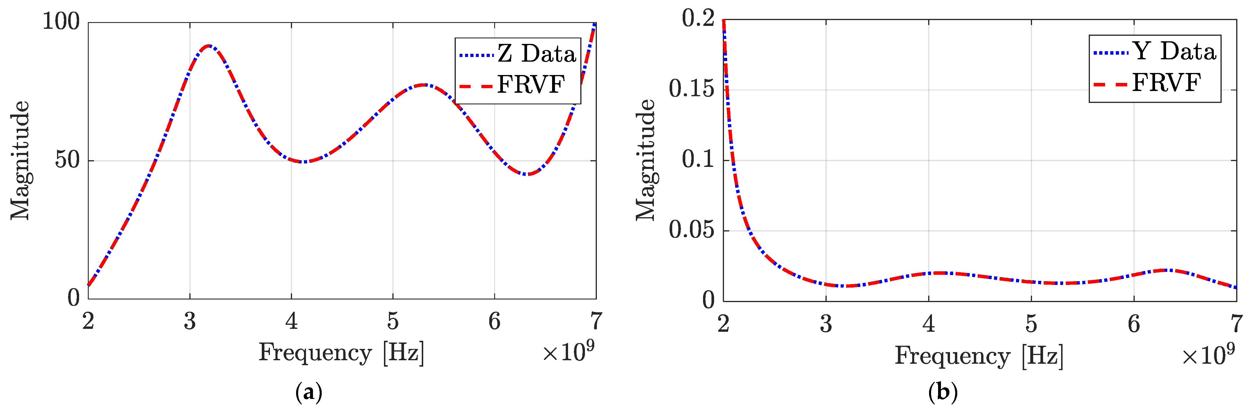
2.2. Stage II: Equivalent Circuit Model via Vector-Fitting Approach

2.2.1. Vector-Fitting Approximation Principle

An antenna’s total performance can be defined using a rational transfer function, allowing it to be coupled with other components in a communication system instead of being built as an isolated component. The first step is to approximate the simulated or measured frequency domain response data rationally. The acquired scattering and admittance parameters versus antenna frequency are estimated using the vector-fitting (VF) approach to rational functions. Vector fitting was first utilized in high-power transformers or electrical power distribution systems, but it was later adapted to higher frequencies, particularly microwaves. Furthermore, it is a robust algorithm able to convert frequency response data to rational functions via a collection of stable poles, ensuring the stability of the approximated rational function, and then enforcing the model’s passivity. The rational approximation of a transfer function H(s) can be expressed as Equation (12):
H ( s ) = n = 1 N r n s p n + d + e s + h s 2 +
If the nonlinearity of Equation (12) is neglected; it can be approximated by the following Equation (13):
H ( s ) n = 1 N r n s p n + d + e s
where s = jω represents the frequency in the Laplace domain, rk and pk denote the kth residue and kth pole, which are either real quantities or complex conjugate pairs and are extracted by the fitting procedure. N presents the order of approximation and the number of poles. while d and e are real terms where d is a constant term, and e is a proportional term.
The vector-fitting method occasionally produces negative residues, resulting in negative element values. In reality, these negative aspects are unusable for design reasons and should be avoided at all costs. Even though these negative elements are not immediately visible, they can be used in modeling and simulation because they allow for accurate, comparable circuits. Furthermore, the negative aspects of the frequency analysis can be easily replicated. So far, extensive research has suggested a different structure, such as a cell with a positive value and a negative resistance. To eliminate nonphysical circuit components, even if the circuit’s guaranteed stability and passivity are enforced, a different circuit representation of the complex poles was proposed in [17].
These new representations have demonstrated that a complex pole pair can be synthesized using RLC lumped elements and a single controlled source [18].

2.2.2. Antenna Modeling Using Vector Fitting

The antenna simulated admittance and impedance versus frequency are exported to Matlab using CST. The data-fitting process is carried out to the 8th order of approximation. It should be noted that the lower orders of approximation produce inaccurate results, and the higher orders of approximation bring a huge circuit.
Figure 4 depicts the approximated fitting rational function using vector fitting (FRVF) and the simulated Y and Z data using CST (data), respectively. It is found that the magnitude of approximated data and original simulated data are in good agreement. It is worth highlighting the vector-fitting algorithm used with passivity enforcement using the technique described in [35]. The previous results are used to generate two equivalent circuit models. Based on the given expressions in [17], the 8th order approximation of the simulated input impedance (Z data) produces four complex pole pairs, which means four parallel R-L-C-G cells connected in series, as reported in Figure 5. In contrast, the same order of the input admittance (Y data) approximation gives two real poles, one with a positive residue, the second with negative residue, and three complex poles pairs. The computed poles correspond to one series RL branch, a positive-valued series cell (RC) combined in parallel with a negative resistance, and three R-L-C-G cells, as illustrated in Figure 6. Figure 7 compares the plots of the obtained S-parameters from CST to those simulated by a SPICE equivalent circuit based on Z data and a SPICE equivalent circuit based on Y data. Figure 7 shows that the extracted models allow a satisfactory approximation of the studied antenna. Overall, these results indicate that the model generated using vector-fitting approximation, based on Z and Y data, reproduces perfect matching results in terms of S11 and input impedance/admittance.

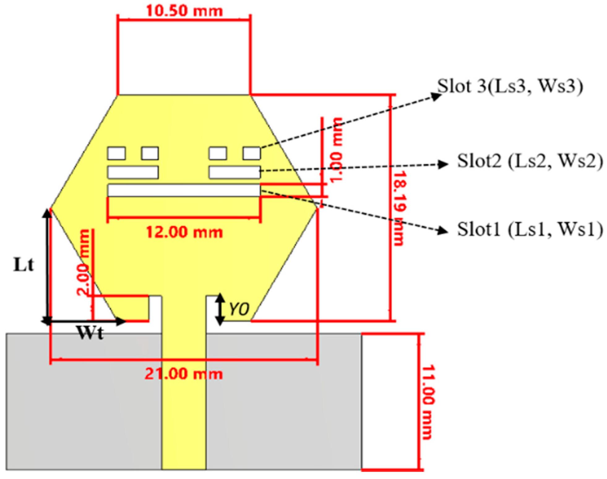
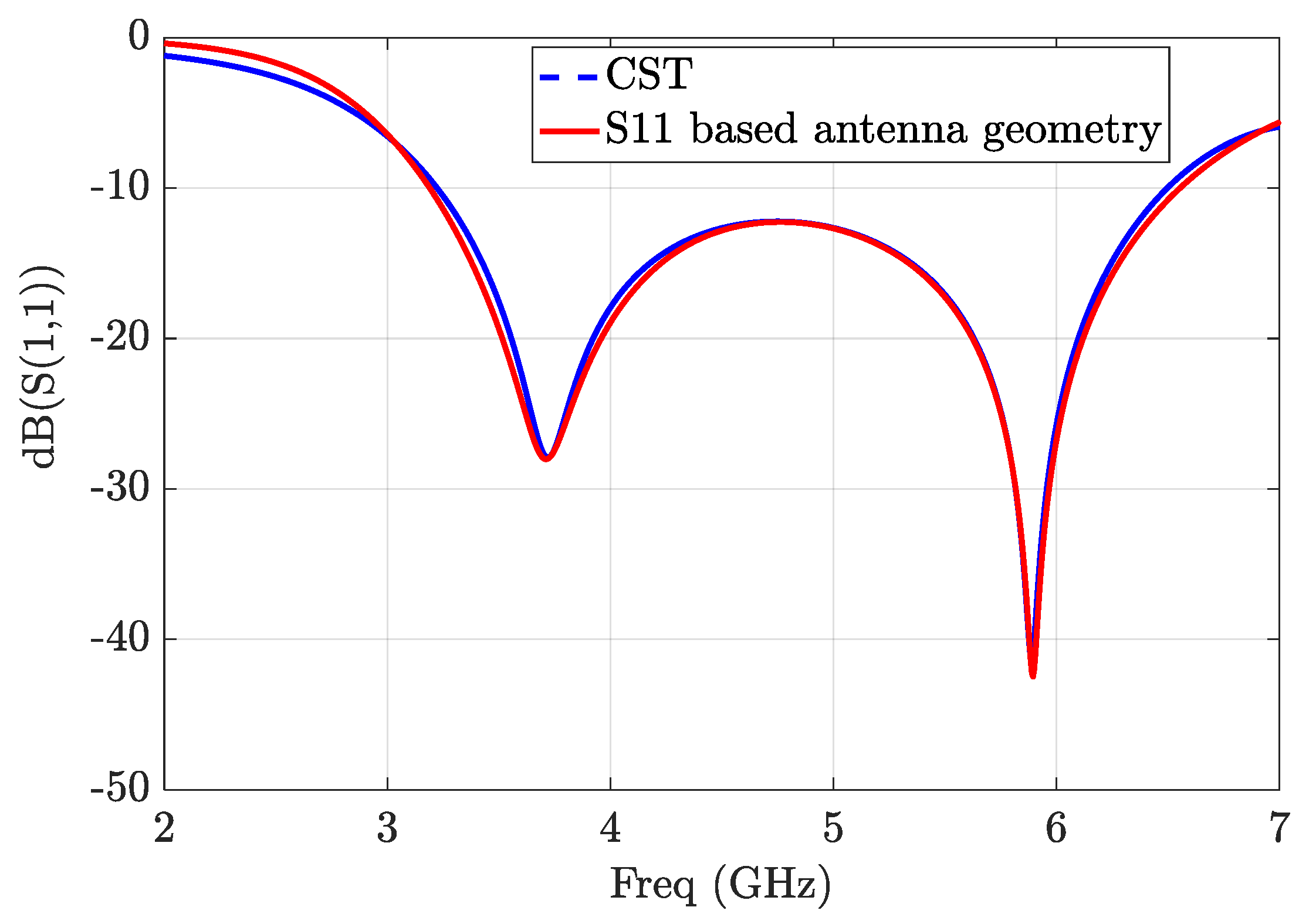
2.3. Equivalent Circuit Based on Antenna Geometry and Substrate Characteristics

The antenna geometry is a combination of a hexagonal patch and Cantor fractal slots of the second iteration. It is observed in Figure 8 that the hexagonal patch can be described as a corner truncated conventional rectangular patch. The equivalent circuit of the conventional patch is formed of resistance (Rp), inductance (Lp), and capacitance (Cp), as described in Figure 8. Those lumped elements are calculated using the following Equations (14)–(17) [15].
C p = ε e f f ε 0 L p W p 2 h cos 2 ( π Y 0 L p )
R p = Q r 2 π f 0 C p
Q r = c ε e f f h f 0
R p = Q r 2 π f 0 C p
where f0 is the design frequency, εeff is the effective permittivity of the substrate, Lp and Wp are the patch length and width, respectively, the Y0 feed point position along the patch length, in the case of the studied antenna, is feeding using an inset feed line, h is the substrate thickness, and c is the light velocity in free space.
The truncated corner effects are described by the capacitance given as Equation (18):
C = ε 0 × ε e f f × S h
S is the surface of the truncated corners defined as Equation (19):
S = 2 × L t × W t
So, the hexagonal patch admittance can be written as Equation (20):
Y p = 1 R p + 1 j ω L p + j ω ( C p + C )
The multifractal Cantor slots and the rectangular partial ground plane are described using a well-known and useful technique. In this technique, the slot is presented through a simple L-C resonator. Equation (21) describes the multifractal slots’ admittance.
Y s = j ω ( i = 1 N C i 1 ω 2 i = 1 N 1 L i )
In the antenna circuit model described in Figure 9, Lf and Cf represent the feed inductance and the antenna static capacitance, respectively. The impedance of the hexagonal patch is modelled by Zp. The Cantor multifractal slots are represented by L-C resonator cells marked Zs, whereas Cc represents the mutual coupling among the radiating patch and the ground plane. The partial ground plane is modelled by L-C resonator as Zdgs. For further understanding, the antenna wideband impedance discontinuities (as described in Figure 1) are introduced in the equivalent circuit and represented by parallel RLC resonators. Using iterative techniques and curve fitting, the tuned values of circuit-lumped elements and the overall antenna equivalent model is shown in Figure 9b. The comparison of S11 response between CST simulation and the equivalent circuit simulation is shown in Figure 10. Based on these results, it can be observed that the computed equivalent circuit model almost perfectly matches the CST results.
To show the accuracy of the generated circuit models, the RMS error for between the antenna results and the results using the computed circuits are plotted in Figure 11. As clearly seen, the generated circuits using a vector-fitting approach allow a satisfactory approximation of the antenna behavior, and the RMS error on the magnitude is 1 × 10⁻⁶ within the operating bandwidth, whilst the circuits synthesized using the Foster approximation based on the antenna impedance data and based on antenna geometry show good accuracy. Consequently, the equivalent circuit model of the suggested design using the vector-fitting approach will be considered in the next study.

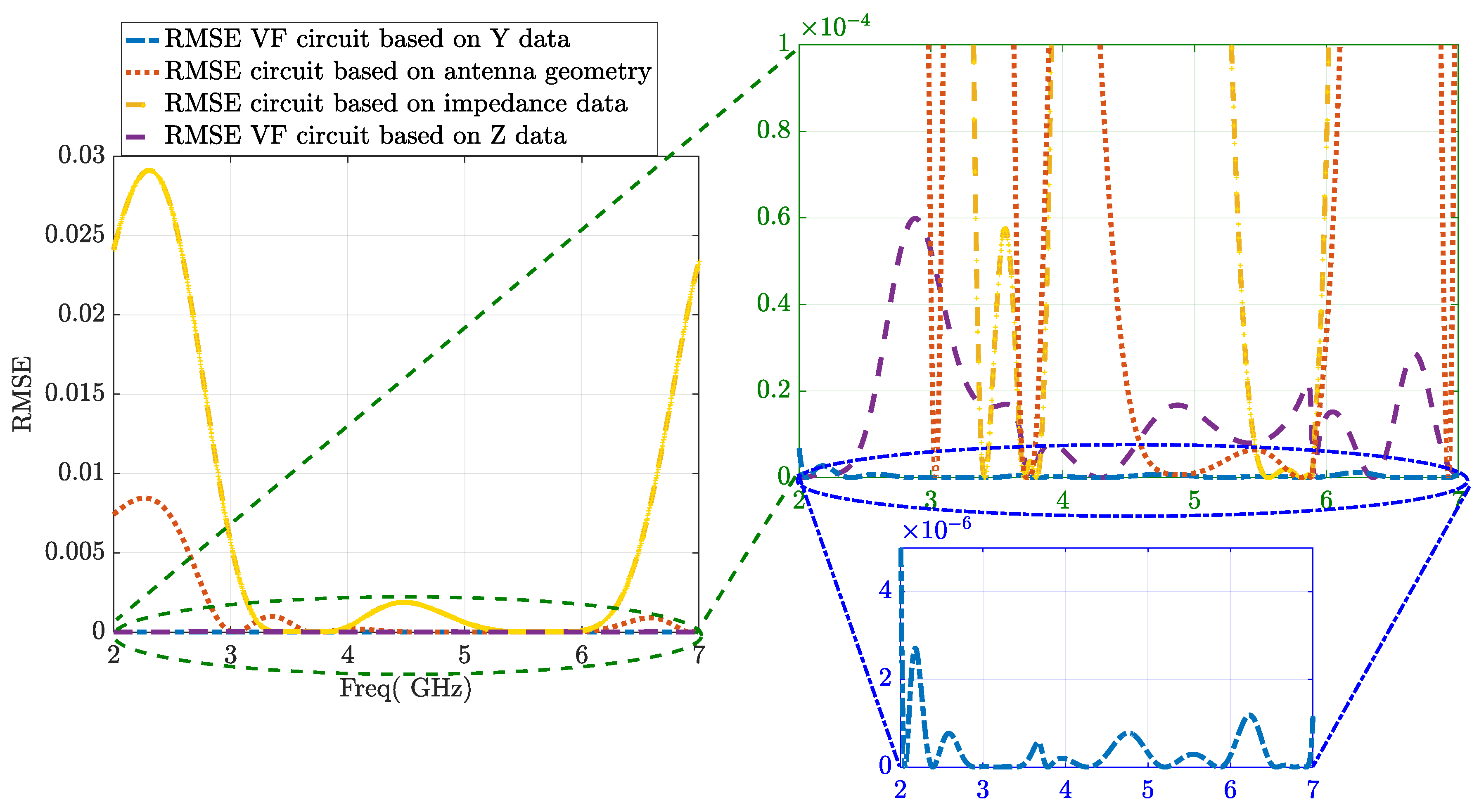
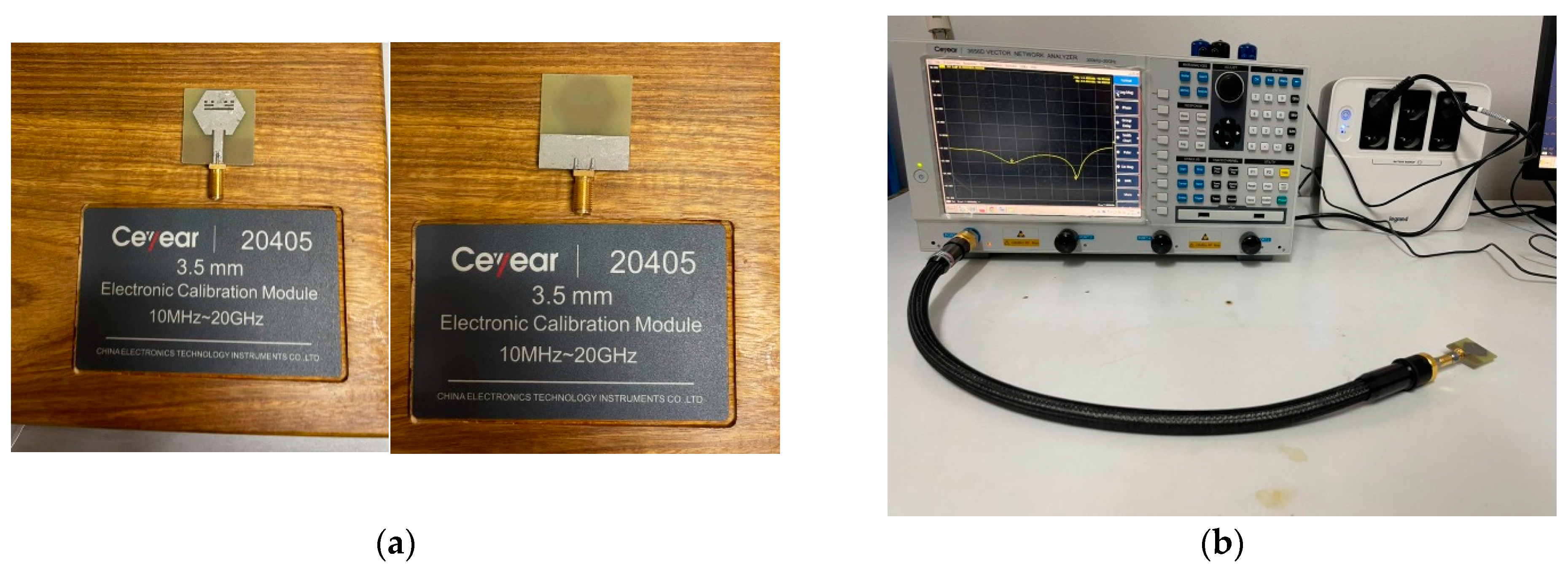
2.4. Prototype, Measurement and Comparison

The prototype of the studied antenna and experimental setup using a Ceyear 3656D VNA are shown in Figure 12.
The comparison of the f S11 response between CST MWS simulation, the equivalent circuits simulations, and the d measurement result are shown in Figure 13. All the results are found in good correlation with each other. One can mention that the simulated results are in close contact with the practical results at the upper resonance frequency of 5.9 GHz, whereas there is a slight difference in S11 values at the lower resonance frequency.

3. Time-Domain Analysis Based on Equivalent Circuit

The pulse generation and shaping procedures are the most crucial tasks in wideband systems design. The pulse waveform determines the signals spectrum characteristic [36,37]. However, several techniques and approaches are discussed in the literature to generate a wideband pulse [36,39]. Different types of pulses can be used for wideband systems, antennas, and circuits. Interestingly, the Gaussian pulse and its derivatives are considered the main choices. The major purpose of this section is to establish the generation technique of the used pulse and the time-domain analysis.

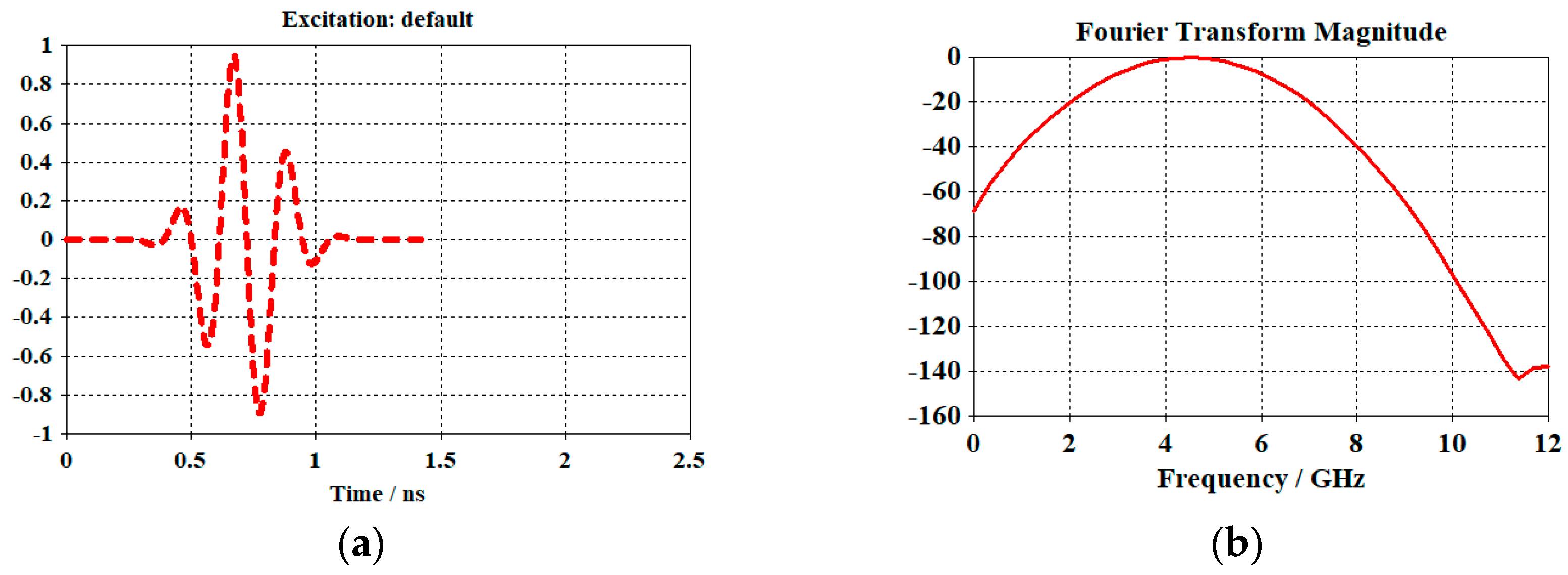
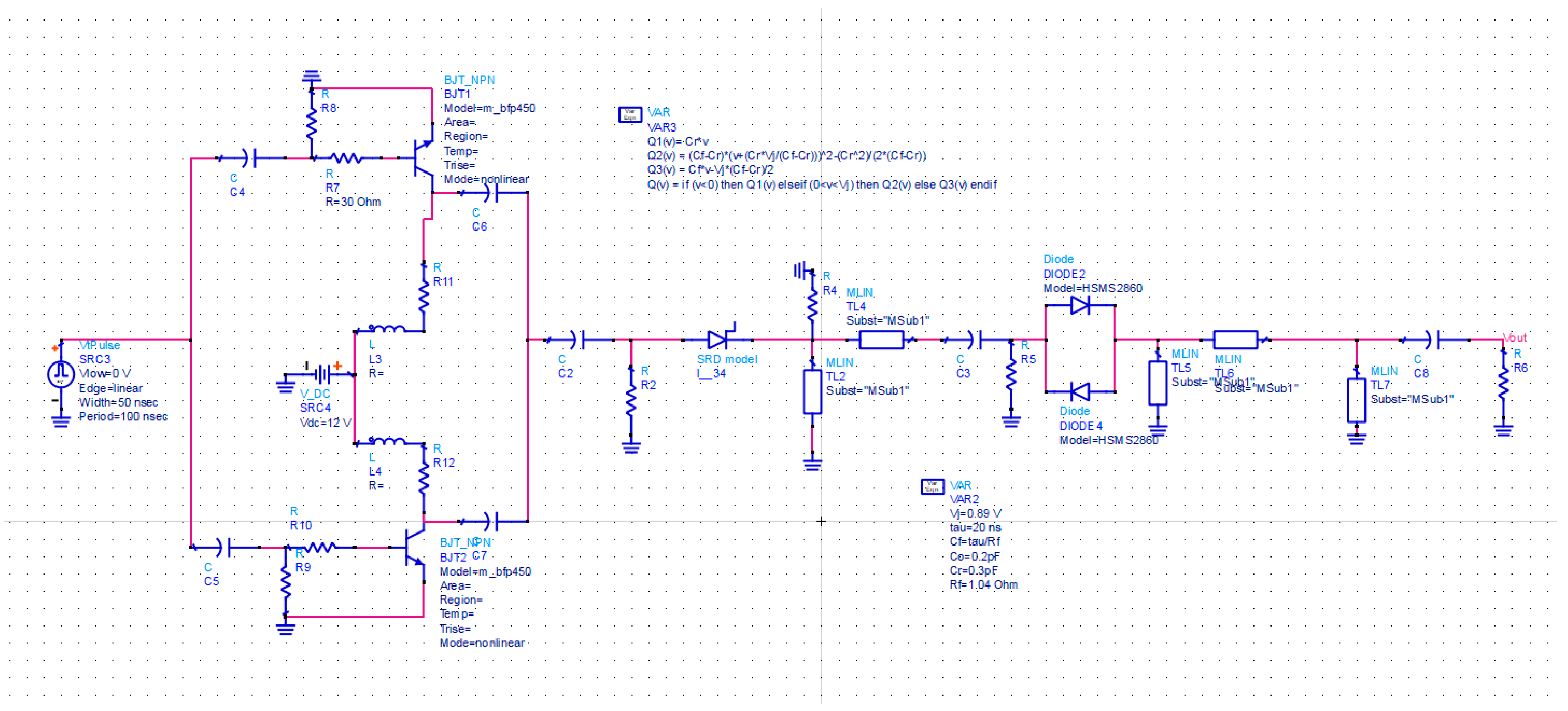
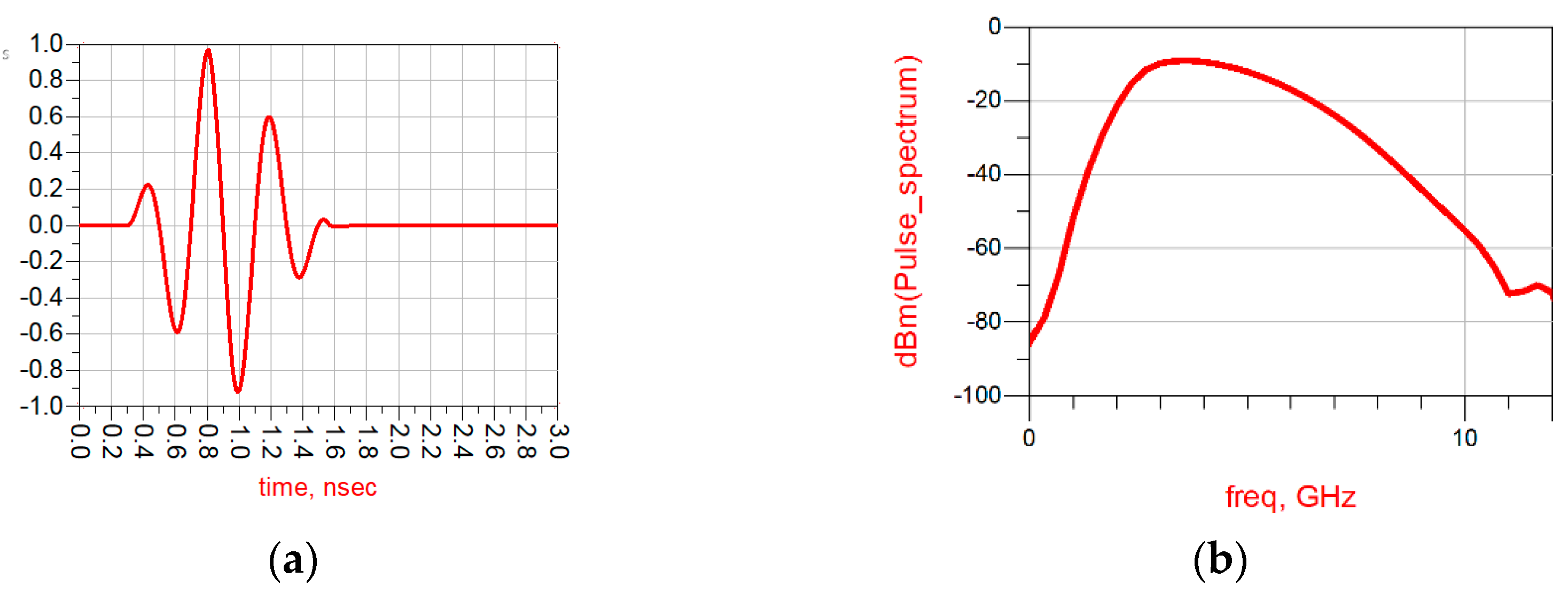
3.1. Pulse Generation Technique

The antenna used is of the ultra-wideband (UWB) kind, and it is true that a high performance in the frequency domain does not guarantee that the antenna will behave well in the time domain. Since this is the case, the seventh Gaussian derivative pulse (Figure 14a) is employed as the antenna excitation signal in CST to provide a desirable time-domain characteristic. Figure 14b shows the power spectral density (PSD) of a Gaussian pulse.
The transistor properties, Schottky diode, and step recovery diode (SRD) are the primary areas of interest for the utilized pulse generator. These pulse generators are not the best option for simple and inexpensive designs because of their size.
The seventh Gaussian derivative pulse generation circuit shown in Figure 15, includes four parts: drive pulse production, SRD [40] pulse sharpening, second derivative pulse forming, and fifth-order derivative RLC. The driver circuit inverts the trigger signal to a driver pulse with high amplitude and sharp edges at its output terminal. Accordingly, the SRD pulse-shaping circuit based on SRD and Schottky diode generate a Gaussian pulse from the driver pulse by combining the negative reflected pulse toward the delay line with the other positive pulse in the terminal load. Then, a second Gaussian derivative pulse circuit forming is employed beside a backward decoupling circuit. This circuit is used to reduce the backward coupling effect and the resulting pulse’s ringing level. Figure 16 describes the considered circuit.
A fifth-order derivative RLC illustrated in Figure 17 is employed to obtain the seventh Gaussian derivative pulse. Figure 18 shows the attained pulse.

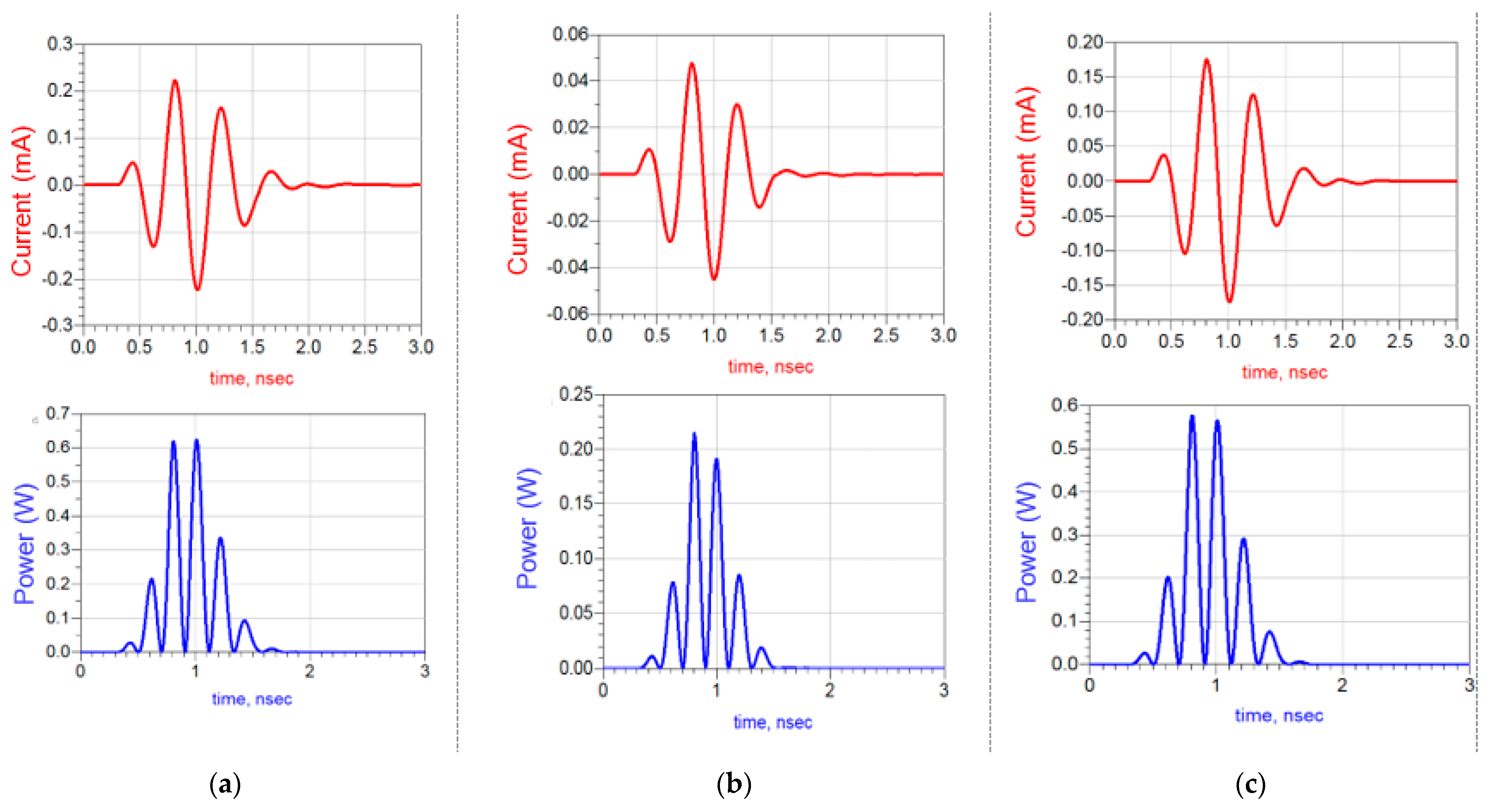
3.2. Antenna Equivalent Circuit Output Results

To make comparisons, the waveform responses of the antenna connected to different loads are demonstrated. It is interesting to note that the pulse carries useful data. Hence, the output pulse is required to match the input pulse with minimum distortions.
The input pulse is compared with the antenna output pulses. The output pulse waveforms are obtained by placing various loads in the terminal of the antenna equivalent circuit. From Figure 19a, it is found that the load of the free space (377 Ohms) has little effect on waveform distortion. The antenna presents good pulse-preserving capability and ensures the correspondence of the input and output waveforms signals after scaling and time shifting. While Figure 19b,c demonstrate that loads of 50 Ohms and 75 Ohms reveal more waveform distortions then more data loss.
To comprehend and appraise the antenna features objectively, each load’s current and power are simulated and plotted versus time and frequency as depicted in Figure 20. Based on these results, it can be clearly seen that the current and power have the same waveforms without any distortions for the tree load, whereas the magnitude depends on the load value.
The output voltage pulse waveform for the different loads is distorted compared with the input pulse due to the antenna band rejection features. It can be clearly seen that the input and output pulses have similar waveforms with distortions. Then, an accurate time-domain feature can be attained using the free space load as a terminal of the antenna equivalent circuit; accordingly, there is less data loss.

4. Conclusions

This work aimed to propose and analyze several techniques and approaches for the formulating of lumped equivalent circuit model of a broadband fractal antenna. A Foster approximation approach was used to extract an equivalent circuit presented by parallel RLC cells connected in series. This method was based on scattering parameters of impedance/admittance data. The objective of the extracted equivalent circuits’ models is to give more details about the impedance behavior in the studied band. Moreover, the vector-fitting approach applied rational function approximation of the antenna simulated impedance data. The equivalent circuit model was extracted from the fitted data. So far, an equivalent model was computed based on the antenna geometry in addition to the multifractal slots and the DGS effects. The obtained results proved that the simulated scattering parameters, impedance/admittance data of the antenna and those of the established equivalent circuits are matched perfectly. The seventh Gaussian derivative pulse was generated using two techniques for further comprehension of the antenna behavior. Then, the antenna equivalent circuit was excited, and a time-domain analysis was performed to check the validity of the antenna pulse response. Overall, these studies highlight that the investigated antenna equivalent circuit models are widely effective in understanding the antenna performance and predicting the effect of integrating antenna with the system. Then, the obtained models can be connected to linear/nonlinear devices or lumped elements in order to analyze electromagnetic circuit problems.

Author Contributions

Data curation, F.E.-z.; Formal analysis, N.O.P.; Investigation, S.A., H.B. and A.G.; Methodology, K.A.B., S.A., A.J.A.A.-G. and N.O.P.; Project administration, N.O.P.; Resources, K.A.B., H.B., A.G. and A.J.A.A.-G.; Software, Fatima F.E.-z., A.J.A.A.-G. and N.O.P.; Supervision, K.A.B. and A.G.; Validation, H.B. and A.J.A.A.-G.; Writing-original draft, Fatima F.E.-z.; Writing-review & editing, S.A. All authors have read and agreed to the published version of the manuscript.

Funding

The authors received no funding for this work.

Conflicts of Interest

The authors declare no conflict of interest.

References

  1. Badawy, M.M.; Malhat, H.A.E.-A.; Zainud-Deen, S.H.; Awadalla, K.H. A Simple Equivalent Circuit Model for Plasma Dipole Antenna. IEEE Trans. Plasma Sci. 2015, 43, 4092–4098. [Google Scholar] [CrossRef]
  2. Garg, M.K. LC Model of Corner Arc Slotted Antenna for C, X and Ku Band Applications. AKGEC Int. J. Technol. 2018, 9, 53–55. [Google Scholar]
  3. Caratelli, D.; Haider, N.; Yarovoy, A. Analytically based extraction of Foster-like frequency-independent antenna equivalent circuits. In Proceedings of the URSI Commission B 2013 International Symposium on Electromagnetic Theory EMTS 2013, Hiroshima, Japan, 20–23 May 2013; pp. 506–509. [Google Scholar]
  4. Ferchichi, A.; Azizi, M.K.; Ali, G. Analysis of a Square Parasitic Antenna by Using Lumped Elements. Int. J. Electron. Telecommun. 2012, 58, 279–283. [Google Scholar] [CrossRef] [Green Version]
  5. Faouri, Y.S.; Ahmad, S.; Parchin, N.O.; See, C.H.; Abd-Alhameed, R. A Novel Meander Bowtie-Shaped Antenna with Multi-Resonant and Rejection Bands for Modern 5G Communications. Electronics 2022, 11, 821. [Google Scholar] [CrossRef]
  6. Yeap, K.H.; Meister, T.; Oh, Z.X.; Nisar, H.; Zhang, Z.; Liu, J.; Su, J.; Song, J.; Gao, Y.; Peng, W.; et al. Circuit Modelling Methodology for Dual-band Planar Antennas. Appl. Comput. Electromagn. Soc. 2021, 36, 1112–1115. [Google Scholar] [CrossRef]
  7. Tuovinen, T.; Berg, M. Impedance Dependency on Planar Broadband Dipole Dimensions: An Examination with Antenna Equivalent Circuits. Prog. Electromagn. Res. 2014, 144, 249–260. [Google Scholar] [CrossRef] [Green Version]
  8. Benkhadda, O.; Saih, M.; Chaji, K.; Ahmad, S.; Reha, A. A Compact Dual-Band CPW-Fed Slot Monopole Antenna for WiFi, WLAN and WiMAX Applications. Arab. J. Sci. Eng. 2022. [Google Scholar] [CrossRef]
  9. Moulay, M.; Abri, M.; Badaoui, H.A. Quad-Band Bowtie Antenna Design for Wireless Communication System Using an Accurate Equivalent Circuit Model. Int. J. Microw. Sci. Technol. 2015, 2015, 1–7. [Google Scholar] [CrossRef]
  10. Palud, S.; Colombel, F.; Himdi, M.; Le Meins, C. Circuit Modeling of a Small Broadband Conical Antenna. IEEE Antennas Wirel. Propag. Lett. 2009, 8, 96–99. [Google Scholar] [CrossRef]
  11. Ali, M.M.M.; Saad, A.A.R.; Khaled, E.E.M. Implementation and justification of a triple frequency-notched UWB proximity-fed antenna with shunt stubs. Microw. Opt. Technol. Lett. 2014, 56, 646–654. [Google Scholar] [CrossRef]
  12. Moradikordalivand, A.; Rahman, T.A.; Ebrahimi, S.; Hakimi, S. An Equivalent Circuit Model for Broadband Modified Rectangular Microstrip-Fed Monopole Antenna. Wirel. Pers. Commun. 2014, 77, 1363–1375. [Google Scholar] [CrossRef]
  13. Yousaf, J.; Jung, H.; Kim, K.; Nah, W. Design, analysis, and equivalent circuit modeling of dual band PIFA using a stub for performance enhancement. J. Electromagn. Eng. Sci. 2016, 16, 169–181. [Google Scholar] [CrossRef] [Green Version]
  14. Ripin, N.; Sulaiman, A.A.; Rashid, N.E.A. An Equivalent Circuit Model of Miniature Double E-Shaped Meander Line Printed Monopole Antenna. J. Telecommun. Electron. Comput. Eng. 2018, 10, 59–63. [Google Scholar]
  15. Akrou, L.; Aghzout, O.; da Silva, H.J.A.; Essaaidi, M. Design of Compact Multiband Antenna with Band-Rejection Features for Mobile Broadband Satellite Communications. Prog. Electromagn. Res. C 2016, 68, 95–106. [Google Scholar] [CrossRef] [Green Version]
  16. Ansarizadeh, M.; Ghorbani, A.; Abd-Alhameed, R.A. An Approach to Equivalent Circuit Modeling of Rectangular Microstrip Antennas. Prog. Electromagn. Res. B 2008, 8, 77–86. [Google Scholar] [CrossRef] [Green Version]
  17. Antonini, G. Spice equivalent circuits of frequency-domain responses. IEEE Trans. Electromagn. Compat. 2003, 45, 502–512. [Google Scholar] [CrossRef]
  18. Tan, W. Modeling and Design of Passive Planar Components for EMI Filters. Ph.D. Dissertation, École Centrale de Lille, Lille, France, 2012. [Google Scholar]
  19. Kim, Y.; Ling, H. Equivalent circuit modeling of broadband antennas using a rational function approximation. Microw. Opt. Technol. Lett. 2006, 48, 950–953. [Google Scholar] [CrossRef]
  20. Sharma, M.; Awasthi, Y.K.; Singh, H. Compact multiband planar monopole antenna for Bluetooth, LTE, and reconfigurable UWB applications including X-band and Ku-band wireless communications. Int. J. RF Microw. Comput. Eng. 2019, 29, e21668. [Google Scholar] [CrossRef]
  21. Duroc, Y.; Vuong, T.-P.; Tedjini, S. A Time/Frequency Model of Ultrawideband Antennas. IEEE Trans. Antennas Propag. 2007, 55, 2342–2350. [Google Scholar] [CrossRef]
  22. Wang, Y.; Li, J.; Ran, L.-X. An Equivalent Circuit Modeling Method for Ultra-Wideband Antennas. Prog. Electromagn. Res. 2008, 82, 433–445. [Google Scholar] [CrossRef] [Green Version]
  23. Saad, A.A.R.; Ali, M.; Khaled, E.E.M. An integrated 3G/Bluetooth and UWB antenna with a band-notched feature. J. Electromagn. Waves Appl. 2013, 27, 2430–2441. [Google Scholar] [CrossRef]
  24. Tuovinen, T.; Berg, M.; Iinatti, J. Analysis of the Impedance Behaviour for Broadband Dipoles in Proximity of a Body Tissue: Approach by Using Antenna Equivalent Circuits. Prog. Electromagn. Res. B 2014, 59, 135–150. [Google Scholar] [CrossRef]
  25. Malekpoor, H.; Jam, S. Analysis on bandwidth enhancement of compact probe-fed patch antenna with equivalent transmission line model. IET Microw. Antennas Propag. 2015, 9, 1136–1143. [Google Scholar] [CrossRef]
  26. Benouakta, S.; Koley, S.; Hutu, F.; Duroc, Y. Considerations on the Equivalent Electric Models of a UHF RFID Helical Antenna Yarn. In Proceedings of the 2019 International Symposium on Signals, Circuits and Systems (ISSCS), Iasi, Romania, 11–12 July 2019; pp. 1–4. [Google Scholar] [CrossRef] [Green Version]
  27. Pordanjani, I.R.; Chung, C.Y.; Mazin, H.E.; Xu, W. A Method to Construct Equivalent Circuit Model from Frequency Responses with Guaranteed Passivity. IEEE Trans. Power Deliv. 2010, 26, 400–409. [Google Scholar] [CrossRef]
  28. Saad, A.A.R.; Salem, D.A.; Khaled, E.E.M. Band-notched UWB Annular Slot Antenna with Enhanced Bandwidth by using EBG Via Holes. Int. J. Commun. 2013, 7, 67–74. [Google Scholar]
  29. Singh, A.; Shet, K.; Prasad, D.; Pandey, A.K.; Aneesh, M. A Review: Circuit Theory of Microstrip Antennas for Dual-, Multi-, and Ultra-Widebands. In Modulation in Electronics and Telecommunications; Dekoulis, G., Ed.; IntechOpen: London, UK, 2020. [Google Scholar]
  30. Kim, Y.; Ling, H. Realisable rational function approximations for the equivalent circuit modelling of broadband antennas. IET Microw. Antennas Propag. 2007, 1, 1046–1054. [Google Scholar] [CrossRef]
  31. Wang, S.; Niknejad, A.; Brodersen, R. Circuit modeling methodology for UWB omnidirectional small antennas. IEEE J. Sel. Areas Commun. 2006, 24, 871–877. [Google Scholar] [CrossRef] [Green Version]
  32. Pandey, A. Practical Microstrip and Printed Antenna Design, 1st ed.; Artech House: Norwood, MA, USA, 2019; p. 443. [Google Scholar]
  33. Biswas, B.; Karmakar, A. Electrical equivalent circuit modelling of various fractal inspired UWB Antennas. Frequenz 2020, 75, 109–116. [Google Scholar] [CrossRef]
  34. Ez-Zaki, F.; Belahrach, H.; Ghammaz, A. Broadband microstrip antennas with Cantor set fractal slots for vehicular communications. Int. J. Microw. Wirel. Technol. 2020, 13, 295–308. [Google Scholar] [CrossRef]
  35. Mahanta, P.K.; Yamin, N.; Zadehgol, A. Passivity verification and enforcement-A review paper. Int. J. Numer. Model. Electron. Netw. Devices Fields 2017, 31, e2286. [Google Scholar] [CrossRef]
  36. Valizade, A.; Rezaei, P.; Orouji, A.A. A design of UWB reconfigurable pulse transmitter with pulse shape modulation. Microw. Opt. Technol. Lett. 2016, 58, 2221–2227. [Google Scholar] [CrossRef]
  37. Ma, T.-G.; Wu, C.-J.; Chou, C.-F. An Impulse-Radio-Based Ultrawideband RF Front-End Module with a New Multilayered Microwave Sampler. Prog. Electromagn. Res. 2008, 86, 1–18. [Google Scholar] [CrossRef]
  38. Protiva, P.; Mrkvica, J.; Macháč, J. A compact step recovery diode subnanosecond pulse generator. Microw. Opt. Technol. Lett. 2009, 52, 438–440. [Google Scholar] [CrossRef]
  39. Aristov, V. Mathematical Description of the Operation of a Step-Recovery-Diode-Based Pulse Generator Circuit. Autom. Control Comput. Sci. 2018, 52, 572–580. [Google Scholar] [CrossRef]
  40. Zhang, J.; Raisanen, A. A new model of step recovery diode for CAD. In Proceedings of 1995 IEEE MTT-S International Microwave Symposium, Orlando, FL, USA, 16–20 May 1995. [Google Scholar]
Figure 1. (a) Case study antenna; (b) the simulated antenna S11 (dB) versus frequency; (c) antenna-simulated impedance (Ohms).
Electronics 11 03724 g001aElectronics 11 03724 g001b
Figure 2. Antenna equivalent circuit based on impedance data.
Electronics 11 03724 g002
Figure 3. (a) Comparison of the SPICE equivalent circuit based on impedance and CST S11 results; (b) comparison of the resulting impedance from CST and equivalent circuit.
Electronics 11 03724 g003
Figure 4. Comparison of the fitted rational vector function (FRVF) and simulated data (data): (a) impedance; (b) admittance.
Electronics 11 03724 g004
Figure 5. ADS model of the lumped equivalent circuit based on Z data.
Electronics 11 03724 g005
Figure 6. ADS model of the lumped equivalent circuit based on Y data.
Electronics 11 03724 g006
Figure 7. (a) S11 results from CST and SPICE equivalent circuit models comparison; (b) Zin results from CST and SPICE equivalent models comparison.
Electronics 11 03724 g007
Figure 8. Studied antenna-radiating element.
Electronics 11 03724 g008
Figure 9. (a) Studied antenna simplified equivalent circuit model; (b) studied antenna equivalent circuit model computed under ADS.
Electronics 11 03724 g009
Figure 10. Comparative study of CST and computed equivalent circuit model results.
Electronics 11 03724 g010
Figure 11. Comparative study of the RMSE of CST and computed equivalent circuit model results.
Electronics 11 03724 g011
Figure 12. (a) Studied antenna prototype; (b) the experimental setup.
Electronics 11 03724 g012
Figure 13. Comparative study of S11 response between CST simulation, equivalent circuits simulations, and measurement data.
Electronics 11 03724 g013
Figure 14. (a) The antenna input signal in CST; (b). antenna input signal spectrum.
Electronics 11 03724 g014
Figure 15. Block diagram of the seventh Gaussian derivative pulse generator.
Electronics 11 03724 g015
Figure 16. Second derivative Gaussian pulse circuit.
Electronics 11 03724 g016
Figure 17. Fifth-order derivative circuit.
Electronics 11 03724 g017
Figure 18. (a) Generated pulse, (b) its spectrum in ADS.
Electronics 11 03724 g018
Figure 19. (a) The output voltage of the antenna equivalent circuit connected to 377 Ohm load; (b) the output voltage of the antenna equivalent circuit connected to a 50 Ohm load; (c) the output voltage of the antenna equivalent circuit connected to a 75 Ohm load.
Electronics 11 03724 g019
Figure 20. (a) The antenna equivalent circuit’s current and power waveforms connected to a 50 Ohm load; (b) current and power of the antenna equivalent circuit connected to a 377 Ohm load; (c) current and power of the antenna equivalent circuit connected to 75 Ohm load.
Electronics 11 03724 g020
Publisher’s Note: MDPI stays neutral with regard to jurisdictional claims in published maps and institutional affiliations.

