Article

Next-Generation Hybrid RF Front-End with MoS2-FET Supply Management Circuit, CNT-FET Amplifiers, and Graphene Thin-Film Antennas

1
Department of Information Engineering, Università Politecnica delle Marche, 60131 Ancona, Italy
2
IMT-Bucharest, National Institute for Research and Development in Microtechnologies, 077190 Voluntari, Romania
*
Author to whom correspondence should be addressed.
These authors contributed equally to this work.
Electronics 2022, 11(22), 3708; https://doi.org/10.3390/electronics11223708
Submission received: 14 October 2022 / Revised: 8 November 2022 / Accepted: 10 November 2022 / Published: 12 November 2022
(This article belongs to the Section Microelectronics)

Abstract

:
One-dimensional (1D) and two-dimensional (2D) materials represent the emerging technologies for transistor electronics in view of their attractive electrical (high power gain, high cut-off frequency, low power dissipation) and mechanical properties. This work investigates the integration of carbon-nanotube-based field-effect transistors (CNT-FETs) and molybdenum disulphide (MoS2)-based FETs with standard CMOS technology for designing a simple analog system integrating a power switching circuit for the supply management of a 10 GHz transmitting/receiving (T/R) module that embeds a low-noise amplifier (LNA) and a high-power amplifier (HPA), both of which loaded by nanocrystalline graphene (NCG)-based patch antennas. Verilog-A models, tuned to the technology that will be used to manufacture the FETs, were implemented to perform electrical simulations of the MoS2 and CNT devices using a commercial integrated circuit software simulator. The obtained simulation results prove the potential of hybrid CNT-MoS2-FET circuits as building blocks for next-generation integrated circuits for radio frequency (RF) applications, such as radars or IoT systems.

1. Introduction

Among recent nanotechnology-based integrated circuits, one-dimensional (1D) and two-dimensional (2D) materials have been identified by the scientific community as the most promising solutions for future electronics, such as next-generation radars and wireless telecommunication applications. Indeed, they both offer scalability potential well beyond that of silicon and all other conventional semiconductors.
In detail, 2D materials such as graphene or transition metal dichalcogenides (TMDCs), e.g., molybdenum disulphide (MoS2), hafnium disulphide (HfS2), and tungsten diselenide (WSe2), have gained increasing interest as transistor channel materials in digital applications thanks to their atomic scale thicknesses and suitable bandgaps, which are highly desirable properties for low-power FETs that can be utilised in back-end-of-line non-volatile memory and logic applications to augment conventional silicon technology in the future sub-5 nm tech nodes [1,2,3,4,5,6,7,8,9,10,11].
At the same time, 1D materials, such as carbon nanotubes (CNTs) deployed in variable capacitors for tunable microwave filters [12] or as channel material for building CNT-based field-effect transistors (CNT-FETs), have demonstrated to be well suitable for mixed-signal and RF applications with respect to both conventional bulk semiconductors and 2D materials [13,14,15,16,17,18]. This is due to the fact that the 1D transport mechanism in CNTs leads not only to a low scattering rate and high current-carrying capability but also, under some conditions, to a linear I D V GS characteristic [19,20,21], as it was also confirmed by electromagnetic and quantum simulations that are supposed to mimic the actual technology used for circuit manufacturing, as carried out in [22], where a compact CNT-FET model was derived. This I–V behaviour could be considered an advantage in future mobile communication systems, where increasingly complex modulation techniques are expected to be used, e.g., in radars or cutting-edge Internet-of-Things (IoT) applications [23].
The implementation of a transmitting/receiving module (T/R) using 1D and 2D materials at 10 GHz is a real challenge. A T/R module implies at least an antenna connected to (i) a high-power amplifier (HPA) for the transmitter side and (ii) a low-noise amplifier (LNA) for the receiver side. These two functions are monitored by a power management module, whose principal function is to disconnect inactive circuits to minimise the power dissipation. The implementation of such circuits implies the utilisation of different 2D materials, depending on their specific physical properties at microwaves and the possibility to grow them at the wafer scale. In this paper, we have used a nanocrystalline graphene (NCG)-based patch antenna at 10 GHz, the NCG thin film having a thickness of 110 nm and a bulk conductivity of 16,000 S/m, thus much thinner than any metal used for metallic antennas to prevent skin depth effects. The NCG-based patch antenna can be grown at the wafer scale on SiO2 thermally grown on a 4-inch high-resistivity silicon (HRSi) wafer. Excellent performance has already been obtained with such antennas in array configuration at 24 GHz [24]. However, the amplifiers cannot be fabricated using graphene monolayers or thin films, since the reproducibility of the circuits is still an unsolved problem. The state of the art is an amplifier at 10 GHz with a gain of 4.2 dB [25], selected out of other thirteen devices and showing a wide variation of its main key performance indicators. Therefore, in this manuscript, we used FETs based on aligned semiconducting CNT arrays, thanks to (i) their high reproducibility when they are grown on SiO2/HRSi wafers and (ii) their low contact resistance [26]. CNTs are folded graphene nanomaterials, and FETs based on them exhibit very good performance at microwaves [27] up to 100 GHz [28] and have already proved to be good candidates to build RF amplifiers [29,30,31,32,33]. Yet, the very properties that make CNT-FETs promising for RF applications, such as their excellent linearity, make them not very suitable for power switching applications, as those needed in the power management block, since it is essentially a DC unit. For it, a high-side power switching circuit based on MoS2-FETs, since they show an impressive on/off ratio [34] and are low-power transistors [35], seems more appropriate and was indeed designed and included in the performed simulations.
This paper is organised as follows. Section 2 is dedicated to describing the whole system architecture together with details of the design of its sub-blocks, namely the supply management circuit using MoS2-FET as power switches, the CNT-FET HPA, and the CNT-FET LNA, both loaded by an NCG-based patch antenna. In Section 3, the simulation results of the whole hybrid system are reported and discussed. Finally, Section 4 concludes the work and gives details about future research and perspectives.

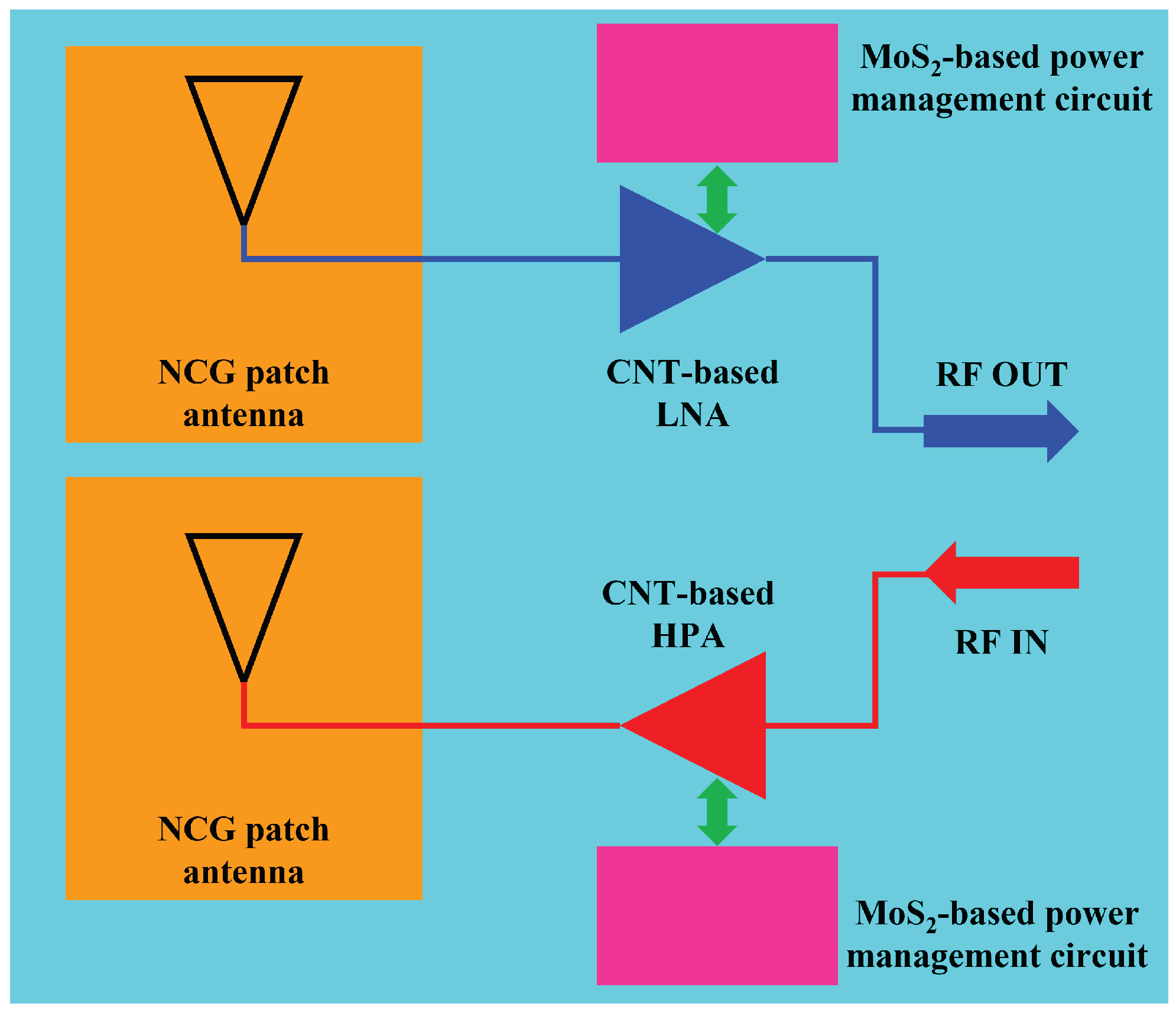
2. System Implementation

The entire T/R module is represented schematically in Figure 1.
It is composed of two independent chains. The RX chain starts with the receiving patch antenna that feeds the LNA, whose power can be cut off when not needed by the high-side switch in the power management circuit. Similarly, the TX chain starts with the HPA that feeds the transmitting patch antenna, and another high-side power switch controls the amplifier operation. This dual antenna configuration avoids the necessity of an RX/TX RF switch and its associated losses.
The RF systems’ performance mainly depends on their front-end amplifiers, e.g., the LNA and HPA. So far, only very few CNT-FET RF amplifiers have been manufactured. The first amplifiers with reasonable gain above 1 GHz were published in [36] and, in the last year, prototypes of RF amplifiers up to 18 GHz have been constructed in [37]. The design of these building blocks is usually implemented through circuit simulators that use compact models representing the actual devices on a given technology. Once the device compact models have been validated through actual experimental measurements, an excellent agreement between physical circuit performance and simulation results should be expected. With this considerations in mind, we designed both the LNA and HPA using the widely acknowledged Stanford CNT-FET model, which was tuned to our technology and to which a noise model was added as in [30].
In the following, a detailed discussion of the design and models used for the different parts is given.

2.1. MoS2-FET Power Controller

MoS2-FET devices exhibit interesting characteristics that should make them ideally suited to build relatively low-speed (with respect to the RF transistors) but higher-efficiency power switches. They were thus used to selectively cut the power to the RF amplifiers, so that the LNA and HPA can individually be enabled or disabled according to the requirements of the protocol/application.
In order to design a power switching circuit, including its driving components, we used the Stanford 2D semiconductor (S2DS) transistor model [38] for the MoS2 power transistors to describe their static voltage/current relationship. The S2DS model is a physics-based and data-calibrated model with a freely available Verilog-A implementation [39] suitable to be directly incorporated into standard design tools, and it is derived using a semiclassical drift transport approach that takes into consideration the density of states in the semiconductor, impurities, and traps, but not the diffusion currents, and so leakage will be underestimated. Moreover, although the S2DS model includes some parasitic capacitance effects, given the low activation/deactivation frequency of the power control circuit, basically DC, we can neglect the behaviour of the parasitic capacitances of the transistors, as the dynamic performance of the switch will be dominated by the bypass capacitors on the supply lines of the amplifiers it powers, as will be seen in Section 3.
For our power switching needs, the S2DS model main parameters, namely the sizes W and L, threshold V T , and the two parasitic resistances due to contacts ( R C ) and leakage ( R L ), were adjusted to match what is expected from higher-current devices, as listed in Figure 2a. R L was actually added to the the S2DS model, and it represents a resistance in parallel between the drain and source terminals introduced to model the leakage that can be expected from such larger devices. These parameters yield the voltage characteristics shown in Figure 2b. With these devices, higher drain voltages than those shown might cause breakdown and should be avoided.
Taking into consideration the fact that these FETs need a negative gate voltage to be turned off and are limited on the maximum V DS voltage, and the amplifiers, as will be shown later, need a 1.5 V supply voltage, we designed a gate drive circuit to bias the power FETs based on a voltage shifter (to adapt the logic control signal to the gate drive requirements) and a discrete inverter to control the output discharge transistor, as seen in the highlighted dashed red box in Figure 3, where the complete schematic of the power switching circuit is reported. The power components of the circuit, M1 and M2, are, respectively, a power MoS2-FET pass element that should interrupt the current to the load and an output discharge MoS2-FET that drains to ground the pass element leakage current and helps to quickly discharge the load capacitance.
As derived from simulations, the required gate voltage swing for optimum operation of the MoS2 devices is about from 1  V to + 2  V, which exceeds their maximum drain voltage handling capability. We thus chose to build the gate drive circuit using standard off-the-shelf MOSFET components, which also allows greater flexibility in the final optimisation of the whole system. Considering the current handling capability, the system has been designed to deliver a supply voltage V DD = + 1.5  V to the amplifiers from a global V SUPPLY = + 2.0  V power supply (which corresponds to the maximum blocking voltage of these MoS2-FETs), with a drop V DS = V SUPPLY V DD across the MoS2-FET. This shall enable the reference transistor to sustain around 4 mA of current if biased with the maximum V GS , but such a high voltage is not easily achievable. Indeed, we can assume to use a V CC = 3 V logic system for the digital signals, and drive the M1 gate with the same voltage to limit the number of power rails in the system. This leads to a driving voltage V GS = V CC V DD = 1.5 V , which yields (according to the simulations shown before) an I D @ V DS = 0.5 V = 3.41 mA , and M1 must then be scaled so that its I D matches the DC current drawn by the load (amplifiers) as determined in the next section, plus the leakage of M2.
Having sized the MoS2 FETs, it is easy to size the rest of the circuit. The driving circuit must be designed to provide the gate voltages for the high-side power switch M1 ( V HI ) and the low-side discharge FET M2 ( V LO ). V HI should swing from 1 V (OFF) to + 3 V (ON), while V LO should swing from + 2 V (OFF) to 1 V (ON).
This is achieved by MD1, which acts as a voltage translator that lowers the digital low level at the input V CTRL from 0 V to V NN = 1  V, while allowing the high level to pass through unaltered, so that the high level on V HI equals the digital supply V CC . V LO is then obtained by inverting V HI , and its high level is set by the resistor divider RD2/RD3 to + 2  V so that V PP can be connected to the same rail as V CC since V LO H = V NN + ( V PP + V NN ) R D 3 / ( R D 2 + R D 3 ) = + 2  V simply imply R D 3 = 3 R D 2 .
A simulation of the whole circuit is shown in Figure 4, which also reports the output voltage driven to loads corresponding to the DC current consumption of the RF amplifiers. To achieve that, i.e., 6.67 mA for the HPA, an M1 2.1 times the reference FET is needed (accounting for leakages), whereas an M1 6.0 times the reference FET is required to drive the 20 mA needed by the LNA.

2.2. CNT-FET Amplifiers

As previously stated, CNT-based transistors have interesting properties in terms of linearity and mobility that make them particularly well-suited for high-frequency amplifier realisation. We thus designed both the LNA and HPA for the T/R module with this type of transistors, using the Verilog-A implementation [40] of the Stanford CNT-FET model [41,42] for the simulations, with parameters tuned to the technology that is being developed to build these devices, and with an added noise model as in [30].
As an indication of the type of performance we can expect from these transistors, Figure 5 reports the output characteristics of the FET used as the input stage of the LNA. Its transition frequency f t , simulated using the intrinsic capacitances included in the Stanford model, was found to be around 45 GHz.
In the design of the CNT-FET HPA we chose to employ a cascode configuration because it combines the high gain of a common-source (CS) topology with the higher operating frequencies of the common-gate (CG) topology, and therefore it is of interest in RF applications. The schematic of the proposed CNT-FET HPA is shown in Figure 6.
More in detail, the cascode topology formed by transistors M1 and M2 helps to reduce the Miller effect of M1 and to obtain excellent reverse isolation, high gain, and improved stability. The degeneration inductor L2 at the source of M1 is used to provide the input resistive impedance without physical resistor for optimum matching. However, increasing the value of L2 reduces the gain of the amplifier. The value of L2 in this design is set at 195 pH. For the inductors, we designed the circuit with the conservative assumption that the technology with which it will be implemented allows the realisation of inductors with a quality factor Q of at least 10. The CNT-FETs M1 and M2 are chosen with the same geometry consisting in a channel width W of 200 µm and channel length L of 200 nm.The power consumption is designed to be 10 mW from a 1.5 V power supply.
The input-matching network was designed by adding the series of C1 and L1 to match the 50  Ω resistance. The output is loaded with an inductor L3 of 800 pH to increase the gain at 10 GHz. The output-matching network to 50  Ω was designed by using L3, C2, L4, and C3. The resistor R1 provides the M1 DC gate bias.
Two typical architectures, the CS and CG topologies, are usually adopted for the design of the first stage of an LNA due to the input-matching and noise characteristics of the circuit. A wideband input matching could be provided by the CG topology at the expense of high noise figure (NF) [43]. The advantage of the CS topology consists in higher gain, but compromises need to be made between gain and broadband input matching.
With these considerations in mind, we chose to employ a cascode LNA because it combines the high gain and low NF of a CS topology with the higher operating frequencies of the CG topology, and therefore it is of interest in RF applications. In this particular application, we used a resonant load for the cascode amplifier because it is important to increase the first stage gain to minimise the overall noise figure. Because of the very high resistance of the resonant load, we added an output common drain stage to help match this to the 50  Ω output load. The schematic of the CNT-FET LNA is shown in Figure 7.
The CNT-FETs M1 and M2 of the first stage are chosen with the same channel width W = 100 µm and channel length L = 200 nm. For the second stage, an M3 transistor of W = 400 µm and L = 200 nm was chosen. The power supply is designed to be a 1.5 V. The input-matching network was designed by adding the series of C1 and L1 to match the 50  Ω resistance. The resistors R1 provides the DC gate bias for M1. The interstage matching was implemented through L4 along with the load inductor L3 optimised to increase the gain at 10 GHz. The resistors R2 and R3 were added for stability purposes. The second stage, represented by the transistor M3 in common-drain configuration, was designed along with the matching network L5, C3, and L6 to adapt the output to 50  Ω .

2.3. NCG-Based Patch Antenna

In order to simulate a realistic T/R module, at least an antenna is necessary for both the transmitter and the receiver side. The validation of the proposed concept of hybrid integration of 1D and 2D materials into a 10-GHz front-end can be achieved by considering two single NCG-based patch antennas, one connected to the CNT-FET HPA (in transmitting mode) and one connected to the CNT-FET LNA (in receiving mode), as displayed in Figure 1. A more sophisticated solution will comprise a full antenna array, which also allows increasing the overall gain (taking into account that NCG-based antennas exhibit a radiation efficiency around 30%).
For this purpose, we started from the fabrication and experimental characterisation of NCG thin films. The deposition was performed by means of a Plasma-Enhanced Chemical Vapour Deposition (PECVD) process using a NANOFAB 1000 (Oxford Instruments, Bristol, UK) as equipment. The HRSi/SiO2 4-inch wafer was covered by NCG using a methane–hydrogen plasma at 900 °C. Then, the electrical characterisation was performed with the four-point probe (4PP) method, based on 4 aligned electrodes: a current is passed through the two outer probes, and the voltage through the two inner probes is measured, allowing the measurement of the sheet resistance. The measured sheet resistance was 579 Ω , from which the thickness of the film was estimated to be approximately 110 nm, whereas the bulk resistance was 6.2 M Ω · cm, which is equivalent to a conductivity of about 16,150 S/m. The Raman spectroscopy showed that the D band/G band intensity peak ratio ID/IG is within the interval 1.5–2.5, which is a proof of the nanocrystalline nature of the material.
The next step was the electromagnetic (EM) simulation of the NCG-patch antenna at 10 GHz using the 3D EM tool CST Microwave Studio, in which the measured electrical characteristics of the NCG thin film were deployed to properly model the material. The results of the simulation are reported in Figure 8. In particular, the 3D layout is displayed in Figure 8b: the patch has overall dimensions of 10 mm × 10 mm, whereas the NCG layer has a width of 5 mm and a length of 4.2 mm. The SiO2/HRSi substrate has a thicknesses of 300 nm/525 µm, respectively, whereas the gold metallisation has a thickness of 500 nm. The chosen configuration is in coplanar waveguide (CPW) technology for (i) ease of integration with the other components of the T/R module, (ii) straightforward on-wafer measurements, and (iii) simple DC biasing of the NCG layer [24]. Figure 8a presents the resulting 2D gain of the antenna as a function of the polar coordinates θ and ϕ , where θ is defined in the ( x , z ) plane and ϕ is defined in the ( x , y ) plane: the maximum (in the broadside direction) is about 2.6  dB, which corresponds to a maximum radiation efficiency of about 16%. Finally, Figure 8c shows the reflection coefficient S 11 in the X band (i.e., 8–12 GHz), exhibiting a clear resonance around 10 GHz, with S 11 = 17.96  dB and a 10  dB-bandwidth of 570 MHz (or, equivalently, a 10  dB-relative bandwidth of 5.7%).

3. Simulation Results

To validate the correct operation and overall performance of the whole system thus designed, several linear, non-linear, and transient simulations were performed. However, before the simulations of the whole system, each individual block was characterised individually, to verify that the system integration does not significantly degrade their performance. Each sub-circuit schematic was thus captured using Cadence Virtuoso® version 6.1.8.210 and simulated using Spectre® version 20.1.0.298. The Verilog-A models of the CNT-FETs and MoS2-FETs were downloaded from [39,40] and adapted to our needs, as thoroughly described in the previous section. The antenna was simulated in CST Microwave Studio 2014, and its S 11 scattering parameters imported into Virtuoso through a Touchstone .s1p data file as a 1-port element, so that the amplifiers see a realistic frequency-dependent load.
Starting from the transmit chain, the scattering parameters of the isolated HPA are shown in Figure 9a, from which it can be seen that a gain of over 10 dB is achieved in the band of interest, while providing good matching at the input and output ports. As expected, the cascode configuration provides very good reverse blocking performance, with an S 12 well below 30 dB.
As far as the output power delivering capability is concerned, Figure 9b shows the input-referred 1 dB compression point. The output power is somewhat limited by the available supply voltage, which restricts the voltage swing of the output device. Nevertheless, about 0 dBm of power can be delivered to the load at the onset of distortion, which corresponds to a drain efficiency of around 10% in linear operation.
A summary of the achieved HPA performances is shown in Table 1, together with a comparison with those obtained by similar works that focus on HPAs made with conventional GaN-based or CMOS standard technologies, since to the best of our knowledge there are not yet any other published results of CNT-based HPAs.
As can be seen, the performances of the CNT-FET HPA are not yet competitive with those obtained by more mature technologies such as CMOS and GaN. Indeed, the CNT technology can be considered still in its infancy compared with the CMOS one, and 1D devices might, due to their peculiar conduction structure, perform less than optimally in higher-power applications.
The behaviour of the whole system, specifically including the power management circuit to which the actual amplifier acts as the load, and with the antenna S 11 model connected to the amplifier output with a 204 pH inductor for impedance matching, was simulated as well. To achieve this, a transient simulation was performed, whose results are shown in Figure 10. Here, the system starts in the OFF condition, with the power manager disabled. The bias and supply voltages are not zero because of the leakage of the MoS2-FET pass element but are low enough to keep the amplifier transistors below threshold. At 1 µs the power manager is enabled, causing the supply and bias voltages to ramp up. The bias voltages are indeed obtained from the supply rail through a simple resistor divider network, with bypass capacitors to shunt the RF signal. The turn-on time is thus dominated by the charging time of those bypass capacitors, and can be tuned to the application requirements by adjusting the divider network resistance (at the expense of increased static power consumption). After the voltages reach a stable state, a 100 mV RF signal source is activated that produces an output power of around 1.2 dBm. The turn-off transient was then simulated as well, this time keeping the RF source activated to verify the isolation capabilities of the amplifier in its OFF state. It is apparent that the power delivered to the antenna immediately drops by about 25 dB, whereas the amplitude of the input signal increases as the input transistor is debiased and so reflects back most of the incoming power.
Other simulations were performed for the LNA, too, whose scattering parameters are shown in Figure 11a, from which it can be seen that a gain of over 28 dB is achieved in the band of interest, while providing good matching at the input and output ports. As expected, the cascode configuration provides very good reverse blocking performance, with an S 12 well below 40 dB. The 1 dB compression point, as shown in Figure 11b, is a bit low but adequate for the input stage given its high gain. The simulated noise figure is reported in Figure 12a, and it is below 1.2 dB around 10 GHz.
A summary of the achieved LNA performance is shown in Table 2, together with a comparison with those obtained by similar works that focus on LNAs made with CNT-FETs, also taking into account some results related to conventional CMOS LNAs.
In particular, with respect to the three CNT-FET LNAs reported in the table, our architecture has the highest gain. The high gain also helped in achieving a low NF, of the same order as the CNT-FET LNAs reported in the table, and at a comparable power dissipation level, and much lower than the CMOS alternatives due to the intrinsic lower noise of the carbon nanotubes versus standard CMOS transistors.
Finally, as regards the NCG-based patch antenna, a thorough comparison was conducted in [24], which highlights its capabilities of providing a simple yet effective reconfigurability of its gain, together with a high fabrication yield and the possibility of tuning the electrical characteristics of the NCG layer by optimising its growth process.
The whole system simulation was also performed in this case, attaching the simulated antenna at the input of the LNA and powering the amplifier through the power switching circuit. A 5 µA current at 10 GHz is considered as the equivalent current source of the incoming radiation at a few meters from the transmitter (by using the well-known Reciprocity theorem), and the noise sources of all the active components and bias resistors were taken into account. The resulting output voltage spectrum is reported in Figure 12b, from which the amplified signal’s first and second harmonics can easily be seen above the noise floor. The overall gain of the whole system results in about 26 dB, which is very similar to the 28 dB obtained by simulating the LNA alone.

4. Conclusions

In this paper, the integration at the design level of different state-of-the-art 1D and 2D nanomaterials with standard silicon CMOS technology for the next generation of RF applications was investigated and simulated. One-dimensional and two-dimensional materials are still in their infancy with respect to the technological maturity of silicon-based electronics, which have approached or already reached their theoretical limits in many aspects. On the contrary, nanomaterials represent a still emerging branch, with a huge potentiality to implement new functionalities and improve their performance. Moreover, a translation of their properties at the macro-scale is always desirable for the practical realisation of components working in the microwave range. Hence, a modular approach envisaging the optimisation of a specific 1D- or 2D-material-based device could be of great help to oversee the potentialities and constraints of each nanomaterial. For all these reasons, in this work, we propose the integration of a proof-of-concept 10 GHz transmitting/receiving module, comprising a power switching circuit for the supply management, a low-noise amplifier, and a high-power amplifier, both designed using CNT-FETs for which the model parameters were tuned from the blueprint and technology data of prototyping devices. In order to complete this T/R module, two nanocrystalline graphene-based patch antennas were used to load or feed the amplifiers.
The obtained simulation results of the overall framework demonstrate that the optimisation of the performance of each part of the T/R module, based on CNT-MoS2-FET hybrid circuits, gives an added value to the performance of modern RF applications, such as radars or IoT systems where low power, high frequency, small size, low weight, and mechanical flexibility are often desired but not always possible when exploiting conventional CMOS technology. Indeed, the designed CNT-FET LNA, despite the infancy of the CNT technology for which it was tuned, already exhibits a very good performance: a gain of over 28 dB with a noise figure of just 1.2 dB. This performance is in line with other published CNT-based LNAs and much better than the referenced CMOS-based LNAs, proving the advantage of using 1D materials for critical amplification tasks. On the other hand, the CNT-FET HPA we were able to design, with a gain just above 10 dB and an output power of 3 dBm at saturation, is not on par with standard CMOS technology or more advanced technologies such as GaN-on-Si or GaN-on-SiC. This can be ascribed to the fact that the 1D technology is in its early stages. After all, this is, to the best of our knowledge, the first attempt at making an HPA out of CNT-based transistors, and knowing its limitations can still be useful.
Finally, the proposed technique also offers a comprehensive view of the capabilities of a multi-domain approach to multi-physics problems (time, frequency, and nano- and macro-scale), which are harmonised into a circuit model with scalable characteristics and reliable outputs in terms of global system performance.

Author Contributions

Conceptualisation, P.C., G.B., L.M., C.T., M.A., M.D., D.M. and L.P.; methodology, P.C., G.B. and M.A.; formal analysis, P.C., G.B., C.T. and M.A.; investigation, P.C., G.B., L.M., M.A. and M.D.; resources, M.A.; writing—original draft preparation, P.C., G.B., M.A. and M.D.; writing—review and editing, P.C., G.B., L.M., C.T., M.A., M.D., D.M. and L.P.; visualisation, P.C., G.B. and M.A.; supervision, C.T., M.D. and L.P.; project administration, L.P.; funding acquisition, M.D. and L.P.; All authors have read and agreed to the published version of the manuscript.

Funding

This research was supported in part by the European Project “NANO components for electronic SMART wireless circuits and systems (NANOSMART)”, H2020—ICT-07-2018-RIA, Grant No. 825430, and in part by a grant of the Romanian Ministry of Research, Innovation and Digitization, CNCS—UEFISCDI, project number PN-III-P4-PCE-2021-0223, within PNCDI III.

Conflicts of Interest

The authors declare no conflict of interest. The funders had no role in the design of the study; in the collection, analyses, or interpretation of data; in the writing of the manuscript, or in the decision to publish the results.

References

  1. Das, S.; Sebastian, A.; Pop, E.; McClellan, C.J.; Franklin, A.D.; Grasser, T.; Knobloch, T.; Illarionov, Y.; Penumatcha, A.V.; Appenzeller, J.; et al. Transistors based on two-dimensional materials for future integrated circuits. Nat. Electron. 2021, 4, 786–799. [Google Scholar] [CrossRef]
  2. Vatalaro, M.; De Rose, R.; Lanuzza, M.; Iannaccone, G.; Crupi, F. Assessment of 2D-FET Based Digital and Analog Circuits on Paper. Solid-State Electron. 2021, 185, 108063. [Google Scholar] [CrossRef]
  3. Chen, X.; Xie, Y.; Sheng, Y.; Tang, H.; Wang, Z.; Wang, Y.; Wang, Y.; Liao, F.; Ma, J.; Guo, X.; et al. Wafer-scale functional circuits based on two dimensional semiconductors with fabrication optimized by machine learning. Nat. Commun. 2021, 12, 5953. [Google Scholar] [CrossRef] [PubMed]
  4. Yu, L.; El-Damak, D.; Ha, S.; Rakheja, S.; Ling, X.; Kong, J.; Antoniadis, D.; Chandrakasan, A.; Palacios, T. MoS2 FET fabrication and modeling for large-scale flexible electronics. In Proceedings of the 2015 Symposium on VLSI Technology (VLSI Technology), Kyoto, Japan, 16–18 June 2015; IEEE: Piscataway, NJ, USA, 2015; pp. T144–T145. [Google Scholar]
  5. Cao, W.; Kang, J.; Sarkar, D.; Liu, W.; Banerjee, K. 2D Semiconductor FETs—Projections and Design for Sub-10 nm VLSI. IEEE Trans. Electron Devices 2015, 62, 3459–3469. [Google Scholar] [CrossRef]
  6. Cao, W.; Kang, J.; Liu, W.; Banerjee, K. A Compact Current–Voltage Model for 2D Semiconductor Based Field-Effect Transistors Considering Interface Traps, Mobility Degradation, and Inefficient Doping Effect. IEEE Trans. Electron Devices 2014, 61, 4282–4290. [Google Scholar] [CrossRef]
  7. Chen, Y.Y.; Sun, Z.; Chen, D. A SPICE Model of Flexible Transition Metal Dichalcogenide Field-Effect Transistors. In Proceedings of the 52nd Annual Design Automation Conference, DAC ’15, San Francisco, CA, USA, 7–11 June 2015; Association for Computing Machinery: New York, NY, USA, 2015. [Google Scholar]
  8. Ahsan, S.A.; Singh, S.K.; Mir, M.A.; Perucchini, M.; Polyushkin, D.K.; Mueller, T.; Fiori, G.; Marín, E.G. A SPICE Compact Model for Ambipolar 2-D-Material FETs Aiming at Circuit Design. IEEE Trans. Electron Devices 2021, 68, 3096–3103. [Google Scholar] [CrossRef]
  9. Estrada, C.J.; Ma, Z.; Chan, M. Complementary Two-Dimensional (2-D) MoS2 FET Technology. In Proceedings of the ESSDERC 2021—IEEE 51st European Solid-State Device Research Conference (ESSDERC), Grenoble, France, 13–22 September 2021; pp. 219–222. [Google Scholar]
  10. Chung, Y.Y.; Cheng, C.C.; Kang, B.K.; Chueh, W.C.; Wang, S.Y.; Chou, C.H.; Hung, T.Y.; Wang, S.Y.; Chang, W.H.; Li, L.J.; et al. Switchable NAND and NOR Logic Computing in Single Triple-Gate Monolayer MoS2 n-FET. In Proceedings of the 2020 IEEE International Electron Devices Meeting (IEDM), San Francisco, CA, USA, 12–18 December 2020; IEEE: Piscataway, NJ, USA, 2020; pp. 40.3.1–40.3.4. [Google Scholar]
  11. Khare, A.; Dwivedi, P. Design, simulation and optimization of multi-layered MoS2 based FET devices. Eng. Res. Express 2021, 3, 045046. [Google Scholar] [CrossRef]
  12. Aldrigo, M.; Dragoman, M.; Iordanescu, S.; Boldeiu, G.; Crippa, P.; Biagetti, G.; Turchetti, C.; Pierantoni, L.; Mencarelli, D.; Xavier, S.; et al. Tunable and Miniaturized Microwave Filters Using Carbon Nanotube-Based Variable Capacitors. IEEE Trans. Nanotechnol. 2022, 21, 118–130. [Google Scholar] [CrossRef]
  13. Moaiyeri, M.H.; Khastoo, N.; Nasiri, M.; Navi, K.; Bagherzadeh, N. An efficient analog-to-digital converter based on carbon nanotube FETs. J. Low Power Electron. 2016, 12, 150–157. [Google Scholar] [CrossRef]
  14. Zanjani, S.M.A.; Dousti, M.; Dolatshahi, M. Inverter-based, low-power and low-voltage, new mixed-mode Gm-C filter in subthreshold CNTFET technology. IET Circuits Devices Syst. 2018, 12, 681–688. [Google Scholar] [CrossRef]
  15. Jooq, M.K.Q.; Mir, A.; Mirzakuchaki, S.; Farmani, A. Design and performance analysis of wrap-gate CNTFET-based ring oscillators for IoT applications. Integration 2020, 70, 116–125. [Google Scholar] [CrossRef]
  16. Schröter, M.; Claus, M.; Hermann, S.; Tittman-Otto, J.; Haferlach, M.; Mothes, S.; Schulz, S. CNTFET-based RF electronics—State-of-the-art and future prospects. In Proceedings of the 2016 IEEE 16th Topical Meeting on Silicon Monolithic Integrated Circuits in RF Systems (SiRF), Austin, TX, USA, 24–27 January 2016; IEEE: Piscataway, NJ, USA, 2016; pp. 97–100. [Google Scholar]
  17. Ramos-Silva, J.N.; Pacheco-Sanchez, A.; Diaz-Albarran, L.M.; Rodriguez-Mendez, L.M.; Enciso-Aguilar, M.A.; Schröter, M.; Ramírez-García, E. High-frequency performance study of CNTFET-based amplifiers. IEEE Trans. Nanotechnol. 2020, 19, 284–291. [Google Scholar] [CrossRef]
  18. Khaleqi Qaleh Jooq, M.; Bozorgmehr, A.; Mirzakuchaki, S. A low-power delay stage ring VCO based on wrap-gate CNTFET technology for X-band satellite communication applications. Int. J. Circuit Theory Appl. 2021, 49, 142–158. [Google Scholar] [CrossRef]
  19. Baumgardner, J.E.; Pesetski, A.A.; Murduck, J.M.; Przybysz, J.X.; Adam, J.D.; Zhang, H. Inherent linearity in carbon nanotube field-effect transistors. Appl. Phys. Lett. 2007, 91, 052107. [Google Scholar] [CrossRef]
  20. Mothes, S.; Claus, M.; Schröter, M. Toward linearity in Schottky barrier CNTFETs. IEEE Trans. Nanotechnol. 2015, 14, 372–378. [Google Scholar] [CrossRef]
  21. Alam, A.U.; Rogers, C.M.S.; Paydavosi, N.; Holland, K.D.; Ahmed, S.; Vaidyanathan, M. RF linearity potential of carbon-nanotube transistors versus MOSFETs. IEEE Trans. Nanotechnol. 2013, 12, 340–351. [Google Scholar] [CrossRef]
  22. Falaschetti, L.; Mencarelli, D.; Pelagalli, N.; Crippa, P.; Biagetti, G.; Turchetti, C.; Deligeorgis, G.; Pierantoni, L. A compact and robust technique for the modeling and parameter extraction of carbon nanotube field effect transistors. Electronics 2020, 9, 2199. [Google Scholar] [CrossRef]
  23. Weller, K. Mobile broadband system evolution and RF technology requirements for user equipment. In Proceedings of the 2008 IEEE Compound Semiconductor Integrated Circuits Symposium, Monterey, CA, USA, 12–15 October 2008; IEEE: Piscataway, NJ, USA, 2008; pp. 1–4. [Google Scholar]
  24. Aldrigo, M.; Dragoman, M.; Iordanescu, S.; Avram, A.; Simionescu, O.G.; Parvulescu, C.; El Ghannudi, H.; Montori, S.; Nicchi, L.; Xavier, S.; et al. Tunable 24-GHz Antenna Arrays Based on Nanocrystalline Graphite. IEEE Access 2021, 9, 122443–122456. [Google Scholar] [CrossRef]
  25. Hamed, A.; Asad, M.; Wei, M.D.; Vorobiev, A.; Stake, J.; Negra, R. Integrated 10-GHz Graphene FET Amplifier. IEEE J. Microwaves 2021, 1, 821–826. [Google Scholar] [CrossRef]
  26. Liu, L.; Han, J.; Xu, L.; Zhou, J.; Zhao, C.; Ding, S.; Shi, H.; Xiao, M.; Ding, L.; Ma, Z.; et al. Aligned, high-density semiconducting carbon nanotube arrays for high-performance electronics. Science 2020, 368, 850–856. [Google Scholar] [CrossRef]
  27. Zhong, D.; Zhang, Z.; Ding, L.; Han, J.; Xiao, M.; Si, J.; Xu, L.; Qiu, C.; Peng, L.M. Gigahertz integrated circuits based on carbon nanotube films. Nat. Electron. 2018, 1, 40–45. [Google Scholar] [CrossRef]
  28. Rutherglen, C.; Kane, A.A.; Marsh, P.F.; Cain, T.A.; Hassan, B.I.; AlShareef, M.R.; Zhou, C.; Galatsis, K. Wafer-scalable, aligned carbon nanotube transistors operating at frequencies of over 100 GHz. Nat. Electron. 2019, 2, 530–539. [Google Scholar] [CrossRef]
  29. Hartmann, M.; Hermann, S.; Marsh, P.F.; Rutherglen, C.; Wang, D.; Ding, L.; Peng, L.M.; Claus, M.; Schröter, M. CNTFET Technology for RF Applications: Review and Future Perspective. IEEE J. Microwaves 2021, 1, 275–287. [Google Scholar] [CrossRef]
  30. Crippa, P.; Biagetti, G.; Turchetti, C.; Falaschetti, L.; Mencarelli, D.; Deligeorgis, G.; Pierantoni, L. A high-gain CNTFET-based LNA developed using a compact design-oriented device model. Electronics 2021, 10, 2835. [Google Scholar] [CrossRef]
  31. Saberkari, A.; Khorgami, O.; Bagheri, J.; Madec, M.; Hosseini-Golgoo, S.M.; Alarcón-Cot, E. Design of broadband CNFET LNA based on extracted I–V closed-form equation. IEEE Trans. Nanotechnol. 2018, 17, 731–742. [Google Scholar] [CrossRef]
  32. Saleem, A.; Alam, M.S.; Moinuddin, A.A.; Armstrong, G.A. Carbon nano-tube field effect transistors for dualband low noise amplifier. In Proceedings of the IMPACT-2013, Aligarh, India, 23–25 November 2013; IEEE: Piscataway, NJ, USA, 2013; pp. 176–179. [Google Scholar]
  33. Makni, W.; Barrage, I.; Samet, H.; Masmoudi, M.; Najari, M. Low noise high frequency CNTFET amplifier. In Proceedings of the 2013 8th International Conference on Design Technology of Integrated Systems in Nanoscale Era (DTIS), Abu Dhabi, UAE, 26–28 March 2013; IEEE: Piscataway, NJ, USA, 2013; pp. 45–49. [Google Scholar]
  34. Hua, Q.; Gao, G.; Jiang, C.; Yu, J.; Sun, J.; Zhang, T.; Gao, B.; Cheng, W.; Liang, R.; Qian, H.; et al. Atomic threshold-switching enabled MoS2 transistors towards ultralow-power electronics. Nat. Commun. 2020, 11, 1–10. [Google Scholar] [CrossRef] [PubMed]
  35. Dragoman, M.; Dragoman, D. Atomic-Scale Electronics Beyond CMOS; Springer: Cham, Switzerland, 2021. [Google Scholar]
  36. Eron, M.; Lin, S.; Wang, D.; Schroter, M.; Kempf, P. L-band carbon nanotube transistor amplifier. Electron. Lett. 2011, 47, 265–266. [Google Scholar] [CrossRef]
  37. Zhou, J.; Liu, L.; Shi, H.; Zhu, M.; Cheng, X.; Ren, L.; Ding, L.; Peng, L.M.; Zhang, Z. Carbon Nanotube Based Radio Frequency Transistors for K-Band Amplifiers. ACS Appl. Mater. Interfaces 2021, 13, 37475–37482. [Google Scholar] [CrossRef]
  38. Suryavanshi, S.V.; Pop, E. S2DS: Physics-based compact model for circuit simulation of two-dimensional semiconductor devices including non-idealities. J. Appl. Phys. 2016, 120, 224503. [Google Scholar] [CrossRef] [Green Version]
  39. Suryavanshi, S.V.; Pop, E. Stanford 2D Semiconductor (S2DS) Transistor Model (Version 1.2.0); nanoHUB, Purdue University: West Lafayette, IN, USA, 2018. [Google Scholar] [CrossRef]
  40. Lee, C.S.; Wong, H.S.P. Stanford Virtual-Source Carbon Nanotube Field-Effect Transistors Model; nanoHUB, Purdue University: West Lafayette, IN, USA, 2015. [Google Scholar] [CrossRef]
  41. Lee, C.S.; Pop, E.; Franklin, A.D.; Haensch, W.; Wong, H.S.P. A Compact Virtual-Source Model for Carbon Nanotube FETs in the Sub-10-nm Regime—Part I: Intrinsic Elements. IEEE Trans. Electron Devices 2015, 62, 3061–3069. [Google Scholar] [CrossRef] [Green Version]
  42. Lee, C.S.; Pop, E.; Franklin, A.D.; Haensch, W.; Wong, H.S.P. A Compact Virtual-Source Model for Carbon Nanotube FETs in the Sub-10-nm Regime—Part II: Extrinsic Elements, Performance Assessment, and Design Optimization. IEEE Trans. Electron Devices 2015, 62, 3070–3078. [Google Scholar] [CrossRef] [Green Version]
  43. Gao, H.; Shi, J.; Lin, F. A wideband LNA with Gm-boosted and noise cancel technique. In Proceedings of the 2020 IEEE International Conference on Integrated Circuits, Technologies and Applications (ICTA), Nanjing, China, 23-25 November 2020; IEEE: Piscataway, NJ, USA, 2020; pp. 17–18. [Google Scholar]
  44. Din, S.; Morishita, A.M.; Yamamoto, N.; Brown, C.; Wojtowicz, M.; Siddiqui, M. High-power K-band GaN PA MMICs and module for NPR and PAE. In Proceedings of the 2017 IEEE MTT-S International Microwave Symposium (IMS), Honolulu, HI, USA, 4–9 June 2017; IEEE: Piscataway, NJ, USA, 2017; pp. 1838–1841. [Google Scholar]
  45. Duffy, M.R.; Lasser, G.; Nevett, G.; Roberg, M.; Popović, Z. A Three-Stage 18.5–24-GHz GaN-on-SiC 4 W 40% Efficient MMIC PA. IEEE J.-Solid-State Circuits 2019, 54, 2402–2410. [Google Scholar] [CrossRef]
  46. Giofrè, R.; Colantonio, P.; Costanzo, F.; Vitobello, F.; Lopez, M.; Cabria, L. A 17.3–20.2-GHz GaN-Si MMIC Balanced HPA for Very High Throughput Satellites. IEEE Microw. Wirel. Components Lett. 2021, 31, 296–299. [Google Scholar] [CrossRef]
  47. Yi, C.; Lu, Y.; Zhao, Z.; Wang, Y.; Zhou, J.; Zhao, B.; Li, P.; Ma, X.; Hao, Y. A 10-W High-Power Amplifier Using Input Nonlinearity for K-Band Satcom Applications. IEEE Microw. Wirel. Components Lett. 2022, 32, 871–874. [Google Scholar] [CrossRef]
  48. Jin, G.; Yan, N.; Lin, Y.; Xu, H. A Linear CMOS Power Amplifier With Efficiency-Optimized Transformer Matching. IEEE Microw. Wirel. Components Lett. 2022, 32, 1059–1062. [Google Scholar] [CrossRef]
  49. Huang, T.W.; Yen, H.C.; Tsai, J.H.; Bai, W.T.; Hung, J.C.; Liang, Y.J. A 19.7–38.9-GHz Ultrabroadband PA With Phase Linearization for 5G in 28-nm CMOS Process. IEEE Microw. Wirel. Components Lett. 2022, 32, 327–330. [Google Scholar] [CrossRef]
  50. Yu, H.; Chen, Y.; Boon, C.C.; Mak, P.I.; Martins, R.P. A 0.096-mm21–20-GHz triple-path noise-canceling common-gate common-source LNA with dual complementary pMOS–nMOS configuration. IEEE Trans. Microw. Theory Tech. 2020, 68, 144–159. [Google Scholar] [CrossRef]
  51. Deng, H.; Feng, H.; Zhang, N. A 0.03–3GHz inductorless wideband low noise amplifier in 65nm CMOS. In Proceedings of the 2020 IEEE 3rd International Conference on Electronics Technology (ICET), Chengdu, China, 8–12 May 2020; IEEE: Piscataway, NJ, USA, 2020; pp. 79–82. [Google Scholar]
Figure 1. Schematic representation of the proposed 1D and 2D material-based T/R module at 10 GHz.
Electronics 11 03708 g001
Figure 2. MoS2-FET model: (a) model parameter values used for the basic power transistor; (b) output characteristics.
Electronics 11 03708 g002
Figure 3. Schematic of the hybrid MoS2-FET power switching topology.
Electronics 11 03708 g003
Figure 4. Simulations of the (a) driver circuit and (b) switch output voltage, performed using a Verilog-A implementation of the MoS2 empirical model described in this work, and a commonly available Vishay Siliconix Si1013CX p-type MOSFET for the driver circuit, for two different loads corresponding to the two currents drawn by the two RF amplifiers.
Electronics 11 03708 g004
Figure 5. Simulated output voltage characteristics of a CNT-FET as used in the input stage of the LNA ( W = 100 µm and L = 200 nm). Its transition frequency f t was found to be around 45 GHz at V GS = 0.7 V and V DS = 1.0 V.
Electronics 11 03708 g005
Figure 6. Schematic of the cascode CNT-FET high-power amplifier.
Electronics 11 03708 g006
Figure 7. Schematic of the cascode—common-drain CNT-FET low-noise amplifier.
Electronics 11 03708 g007
Figure 8. (a) CST Microwave Studio simulated 2D gain of the 10 GHz NCG-based patch antenna whose 3D layout is shown in (b); the angle θ is upon the ( x , z ) plane, whereas the angle ϕ lies on the antenna plane ( x , y ) ; (c) simulated reflection coefficient S 11 of the antenna in the X band.
Electronics 11 03708 g008
Figure 9. Simulations of the HPA input–output scattering parameters (a) and input-referred 1-dB compression point (b).
Electronics 11 03708 g009
Figure 10. Simulations of the transmit chain transient response. The power switch is enabled at time 1 µs for 7.5 µs through VCTRL, as shown in the top panel, whereas a 10 dBm (100 mV) RF input is applied to the HPA after some time to allow for the power and bias voltages to stabilise (middle panel). The bottom panel shows the resulting power delivered to the antenna, which is 1.2 dBm while the transmitter is active.
Electronics 11 03708 g010
Figure 11. Simulations of the LNA input–output scattering parameters (a) and input-referred 1-dB compression point (b).
Electronics 11 03708 g011
Figure 12. Simulations of the LNA noise figure (a) and output voltage spectrum (b), computed using a 2 20 -points FFT over a 819.2 ns long signal window with the antenna feeding 5 µA ( 62 dBm) of current into the LNA. The output voltage fundamental results in 46.1 dBV ( 36.1 dBm), corresponding to an effective gain of 25.9 dB. The noise floor is 160 dBm / Hz .
Electronics 11 03708 g012
Table 1. Performance comparison of the designed HPA with other works.
Reference[44][45][46][47][48][49]This Work
Node200 nm150 nm100 nm100 nm40 nm28 nm90 nm
TechnologyGaN-on-SiCGaN-on-SiCGaN-on-SiGaN-on-SiCMOSCMOSCNT-FET
DataMeas.Meas.Meas.Meas.Meas.Meas.Sim.
BW (GHz)17.2–20.218.5–2417–20.517–20.526.9–33.219.7–38.98.7–11.3
Pout (dBm)4036.54040.417.816.23.0
Gain (dB)2025242314.818.110.3
PAE (%)3840303330.727.310
Table 2. Performance comparison of the designed LNA with other works.
Reference[50][51][43][36][31][30]This Work
Node65 nm65 nm130 nm450 nm32 nm90 nm90 nm
TechnologyCMOSCMOSCMOSCNT-FETCNT-FETCNT-FETCNT-FET
DataMeas.Sim.Sim.Meas.Sim.Sim.Sim.
BW (GHz)1–200.03–30.1–51–1.23–380.01–2.59.75–10.25
Supply (V)1.61.21.22.51.02.01.5
Power (mW)20.35.74.4N/A161830
Gain (dB)12.811.6201113.7–14.727.528.4
NF (dB)3.3–5.32.7–3.323.04–3.9780.4–1.31.01.2
Publisher’s Note: MDPI stays neutral with regard to jurisdictional claims in published maps and institutional affiliations.

