
Mitigation of Thermal Stability Concerns in FinFET Devices †

1
Department of Microelectronics Reliability, Ariel University, Ariel 40700, Israel
2
Microsystems Technology Laboratories (MTL) Department, Massachusetts Institute of Technology, Cambridge, MA 02142, USA
*
Author to whom correspondence should be addressed.
†
This paper is an extended version of our paper published in 2021 IEEE 32nd International Conference of Microelectronics (MIEL) under the title “Self-Heating Effects Measured in Fully Packaged FinFET Devices”, Niš, Serbia, 12–14 September 2021.
Electronics 2022, 11(20), 3305; https://doi.org/10.3390/electronics11203305
Submission received: 6 September 2022
/
Revised: 6 October 2022
/
Accepted: 8 October 2022
/
Published: 14 October 2022
(This article belongs to the Special Issue Advances in Micro- and Nano-Electronics)
Abstract
:Here, we developed a procedure for mitigating thermal hazards in packaged FinFET devices. A monitoring system was installed into devices, based on self-heating impact analysis in the system and device levels, to allow for the observation and alerting of chip temperature and reliability risks. A novel algorithm for reducing measurement noise by means of temperature fluctuation compensation and the filtering of invalid data is presented and demonstrated on packaged devices. The results presented in this work show that the proposed techniques make exceptional improvements to sensory accuracy. Using this methodology enables the mitigation of thermal concerns in systems, including large data servers, and accelerates development of smart resource allocation formations.
1. Introduction
Today, the primary challenge in raising performance in highly scaled silicon devices is thermal management. Aggressive scaling and advances in materials engineering have allowed modern devices to reach potential clock speeds far beyond operation standards. The bottleneck for speed increase arises from overheating concerns due to dynamic power dissipation. With the introduction of three-dimensional (3D)-gate FET devices, the thermal management issue increased.
The Self-heating Effect (SHE) is a significant thermal stress factor in the latest technologies. Self-heating is more severe in all variations of 3D-gate FETs compared to planar FETs, primarily due to the shape of the Fins. In planar devices, heat is dissipated directly through the bulk and contacts. In FinFETs, the heat accumulates at the top of the Fins, dissipating slowly through the bottom of the Fins and out to the substrate and contacts. Additional problems arise in designs such as ultra-thin body silicon on insulator (UTB SOI) devices. In SOI FinFETs the oxide insulator’s thermal conductivity is much lower than that of standardFinFETs [1]. As technology advances with scaling, the Fins continue to become taller and thinner, escalating the heat dissipation problem. As GAAFETs and nanotubes become more popular, there will be more SHE damage since there is more thermal isolation of the channel from the substrate [2,3,4].
Process variations have significant effects on thermal dissipation deficiencies [5]. Some aspects of process variations are die-specific [6]. The consequences of these variations are far reaching for a fraction of devices from a thermal management standpoint. Without individual sensory modules per chip, the location of devices that are especially vulnerable to thermal damage is almost unfeasible.
In this study, we perform a novel procedure for optimizing accuracy in sensing decreases in performance for the continuous self-monitoring of microchips. The study advances efforts detailed in a previous study, where a microchip health monitor (MHM) system for supplying real-time time-to-failure (TTF) assessments of devices was proposed [7]. The monitor was developed based on the assumption that the MTTF of known failure mechanisms can be modeled using a statistical approximation as described in [8]. The objective of this study is to formulate and demonstrate a measurement module that uses advanced methods for noise reduction, and to implement it on the MHM framework. We show that, with the proposed methods, self-monitoring becomes feasible. Systems that lack noise reduction methods produce results that are not dependable enough to make the system beneficial in practice.
This paper has the following outline: in Section 2, we review the technical background on thermal management concerns, both on the device and system levels. We demonstrate how the Multi-Temperature Operational Life (MTOL) testing method [9] was applied to isolate the contribution of self-heating in 16 nm technologies in both spheres. In Section 3, we present the following noise reduction techniques: the tempering of frequency-decrease distortion caused by temperature fluctuations and early degradation data filtering to maximize accuracy. In Section 4, we implement these methods using a novel algorithm in an MPSoC device using 16 nm FinFET technology [10]. Conclusions and suggestions for future work are presented in Section 5.
2. Measuring SHE in the Devices and Systems
To assess the impact of self-heating on the thermal management of the chip, we analyzed the behavior of the mechanism in a previous study [11] in two different resolutions: at the device level and the system levels. In this study, we included the points of that work which help to illustrate the importance of the microchip sensor in FinFET devices. Additionally, new aspects of the study were introduced to add detail and to show plans for future studies.
2.1. Device-Level Testing and Results
Our inspection of SHE at the device level focuses on reliability concerns, namely, the interaction between self-heating and other prominent failure mechanisms. A topic of diverse discussion remains, concerning which mechanisms are predominant. Some papers indicate hot carrier injection (HCI) [12,13] or electromigration (EM) [14] as the prevailing mechanism. SHE propagates from the channel during device transitions, making it current stimulated. It is logical that HCI or EM would be augmented, since they are also current based [15]. This claim is difficult to defend. Finding the relative weight of SHE compared to the other mechanism is not trivial. Additionally, many studies show that bias temperature instability (BTI) dominates in FinFETs compared to HCI and EM [16]. Our findings reveal BTI as the dominant mechanism. SHE is also present, supplementing the effects of BTI at high frequencies. We separate SHE from BTI and highlight its relative weight in the device degradation as a function of operational frequency.
Our study was carried out on a packaged product which enables the failure data of different mechanisms to be proportionally weighted. The long-term effects of SHE were examined by studying the frequency degradation of ring oscillators (RO) in week-long (~175 h) temperature and voltage stress tests. The MTOL testing method was used to isolate the impact of SHE relative to other origins of degradation [17]. A wide span of frequencies (about two orders of magnitude) was produced to identify changes in degradation trends with frequency. Frequency effects are clear evidence of current-caused mechanisms such as HCI or EM. It is well known that at any given core voltage, the transition time (dV/dt) is approximately constant, as is the input capacitance (C) of each successive gate. Hence, the total current through the output inverter will be proportional to:
where “f” is the transition frequency. Rings with low frequencies will have few transitions and, therefore, almost no current flow. The current stress increases with the increase in frequency.
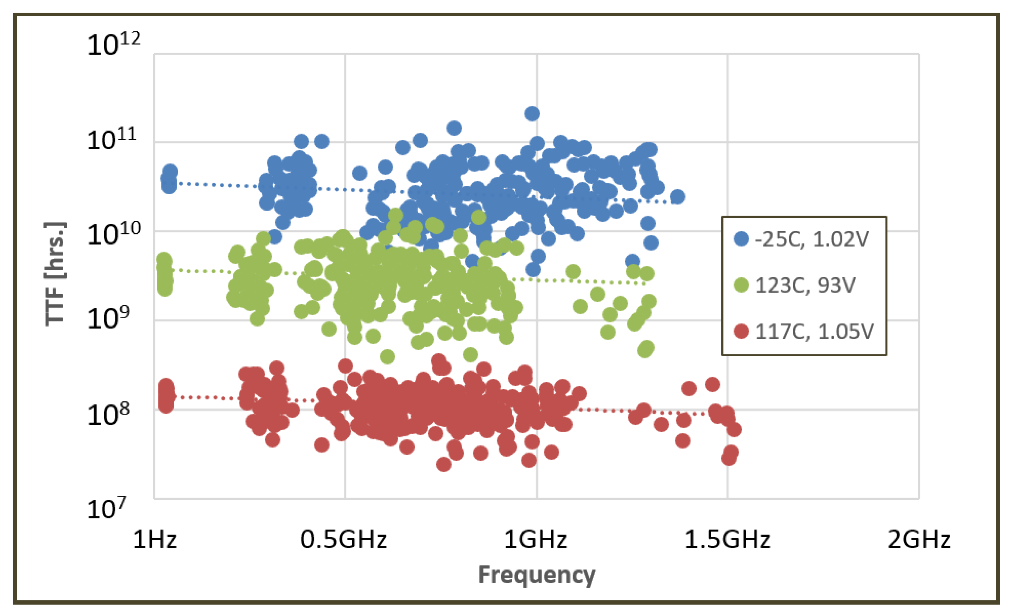
Mechanisms that are caused by voltage and temperature stress, such as BTI, do not change significantly with frequency. Our study showed that there is a linear reduction in TTF with the increase in frequency. The results were reproduced over a large span of temperatures and voltages. Figure 1 displays the effect in three different stress modes. Table 1 provides a summary of the TTF values received in Figure 1 at extreme high and low frequencies.
The results show that the frequency effect is consistent in all the tests with a decrease in TTF to about 75% at a frequency of 1 GHz. The results refute the possibility that the degradation is based on current. If the degradation were current based, the relative effect of frequency to TTF should increase in severity with the increase in stress, as opposed to conserving a similar effect.
The results have a uniform degradation trend. This shows that the degradation in all stress conditions is caused by a single dominant failure mechanism. When the data were set to an Eyring model, the Arrhenius and non-Arrhenius constants extracted were characteristic of BTI. The frequency effect observed was caused by the self-heating effect. With the increase in frequency, heat remained trapped in the fins due to poor thermal diffusivity. The data is plotted to the Eyring model detailed in Equation (2).
γ is the voltage factor and V is the core voltage. is the activation energy; k is Boltzmann’s constant. T is the core temperature in degrees Kelvin. is the frequency-dependent temperature addition caused by SHE. The value of this parameter is found by comparing the TTF of low frequencies to high frequencies. It is represented using the following relationship:
The heat increase is a function of frequency and core voltage (squared as expected with power dissipation). “CLRth” equals: 3.85 × 10⁻⁹ [F·Ω].
Figure 2 is a collection of MTOL test results arranged to reveal the activation energy of the data set. The data shown are a subset of a larger data set, selected with a focus on the change in TTF values with relatively small changes in frequency. The full data set is provided in [11]. The figure is plotted separately for four frequency regimes. The slopes of all the plots (marked with dotted lines) show an activation energy of 0.49 eV, which is characteristic of BTI. It is apparent from the figure that the TTF values decrease with the increase in frequency. Since the EA slope is constant with increased frequency, the decrease in TTF is caused by increased temperature, i.e., enhanced BTI. Since the x-axis is 1/kT, the increase in temperature due to increased frequency shifts the values to the left. When current flows through the channel due to device operation, phonons develop inversely, corresponding to the thermal conductivity [18,19]. Therefore, temperature changes in the devices are proportional to operation frequency [20]. Raising the frequency causes a temperature change, which exacerbates the effects of BTI on the devices. The voltage constant γ for the data set is 11.7, as we explained in [11]. This voltage relationship fits an exclusively BTI degradation characteristic.
When comparing the above results with planar 28 nm technology, we found that BTI is also the dominant mechanism. In contrast, the degradation recorded is “flat” along the range of frequencies (10–700 MHz) [21]. This shows a clear transition in the data between planer and 3D-gate FET devices.
2.2. System-Level Testing and Results
From a system-level perspective, the thermal management hazard of the chip is assessed. This investigation is especially crucial for large chips containing dense arrays of transistors. End-user applications can only be intelligently designed with clear guidelines showing how to avoid overheating [16]. Intuitively, SHE adds to the heat buildup of the complete chip. Our method shows what percentage of chip internal temperature displacement is associated with self-heating. The contribution of SHE is found by taking the offset of the temperature change caused by the increase in frequency, hence the increased current, compared to the increase in logic.
The system-level concern of SHE was assessed based on a standard power dissipation model. Core temperature change directly corresponds with the dynamic power dissipation caused by the logical activity, as shown in Equation (4):
where N is the total number of logic elements and f is transition frequency. CL is the load capacitance, and Rth is the thermal resistance. The testing was carried out by tracking the temperature changes for different FPGA programs created using a variable sum of ring oscillators. The temperature was gauged with the Xilinx Ultrascale+ built-in Sysmon internal temperature sensor [22]. The board was powered using a Regal DP832 power supply [23] to track the current consumed and, therefore, the total board power consumption. Plotting the power versus temperature reveals the thermal resistance, which is 14.45 K/W. The board is retained at an ambient temperature of 25 °C with a thermal chamber.
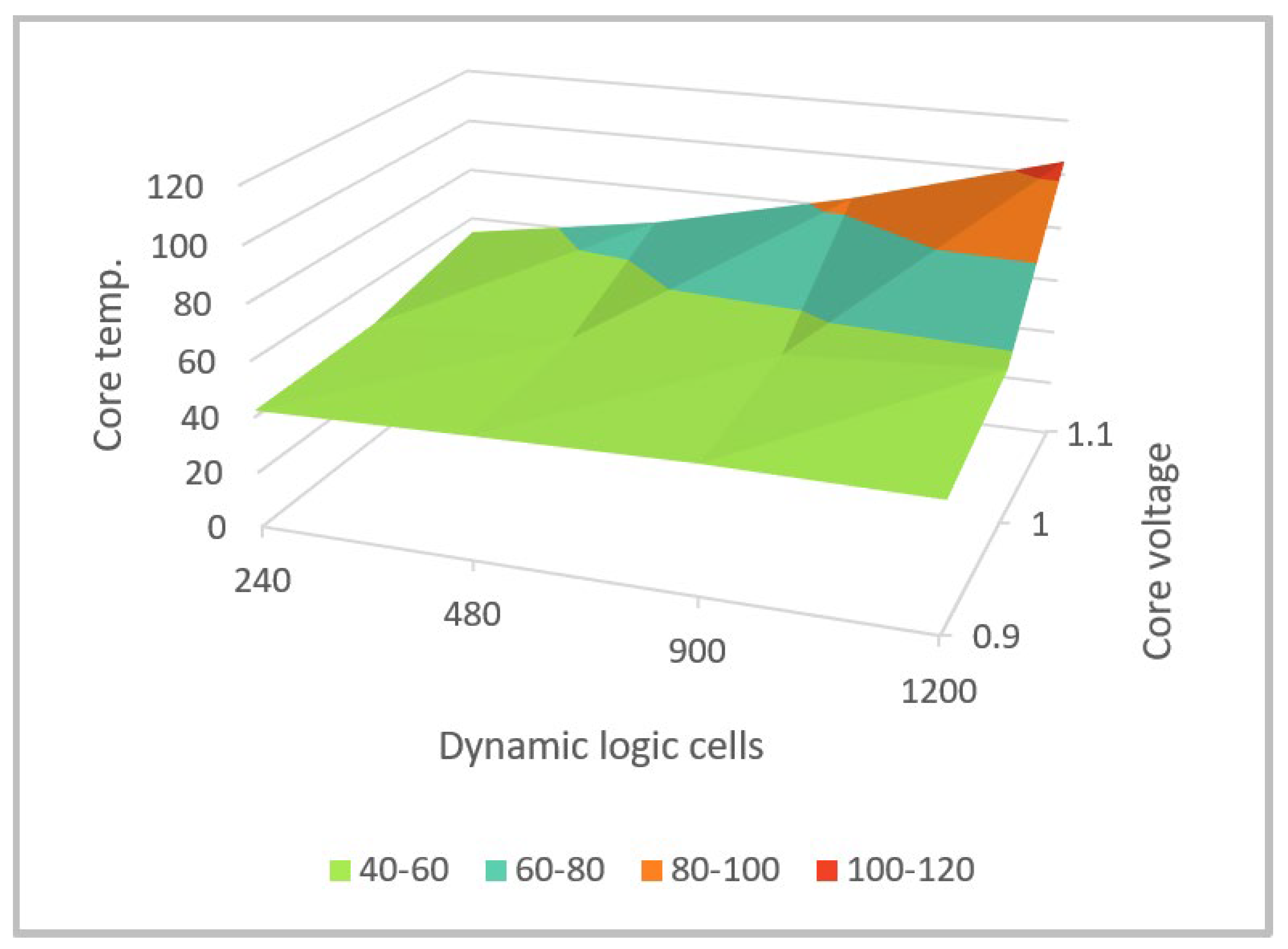
A global perspective of thermal offset due to increased voltage and dynamic logic is displayed in the surface plot in Figure 3. The dynamic activity is produced from three-stage ring oscillators programmed into the FPGA. We show in [11] that that data reveal a load capacitance of about 1.49 pF per cell.
We also compared the temperature increase for added logic to that of increased frequency. Tests were carried out using a constant voltage of 1 V with changes in the number of inverters in the rings. Three-stage rings were compared to thirty-three-stage rings to create a difference of one order of magnitude (1 GHz and 100 MHz, respectively). There is a 37.5% temperature offset from increasing the frequency by one order of magnitude, as we demonstrated in [11]. Temperature changes from 33-stage to 333-stage rings retained to the same ratio, showing a linear increase with frequency. Supposedly, frequency and logical elements should produce an analogous result, as seen in planar 28 nm technology. The nature of SHE, which heats the logical elements during transition times, is appropriate to explain this offset. As mentioned in the previous section, concerning device reliability, we calculated 3.85 × 10⁻⁹ [F·Ω] for load capacitance and thermal resistance. If we estimate that the value of the load capacitance alone is the same as that found in the power dissipation study, we receive a thermal resistance for the FinFET devices of about 7 K/W. The extreme contrast in dimensioning between the base area of a device channel and the area of the chip explains the contrast in the thermal resistance.
2.3. Modification of System-Level Testing Using External Clocking
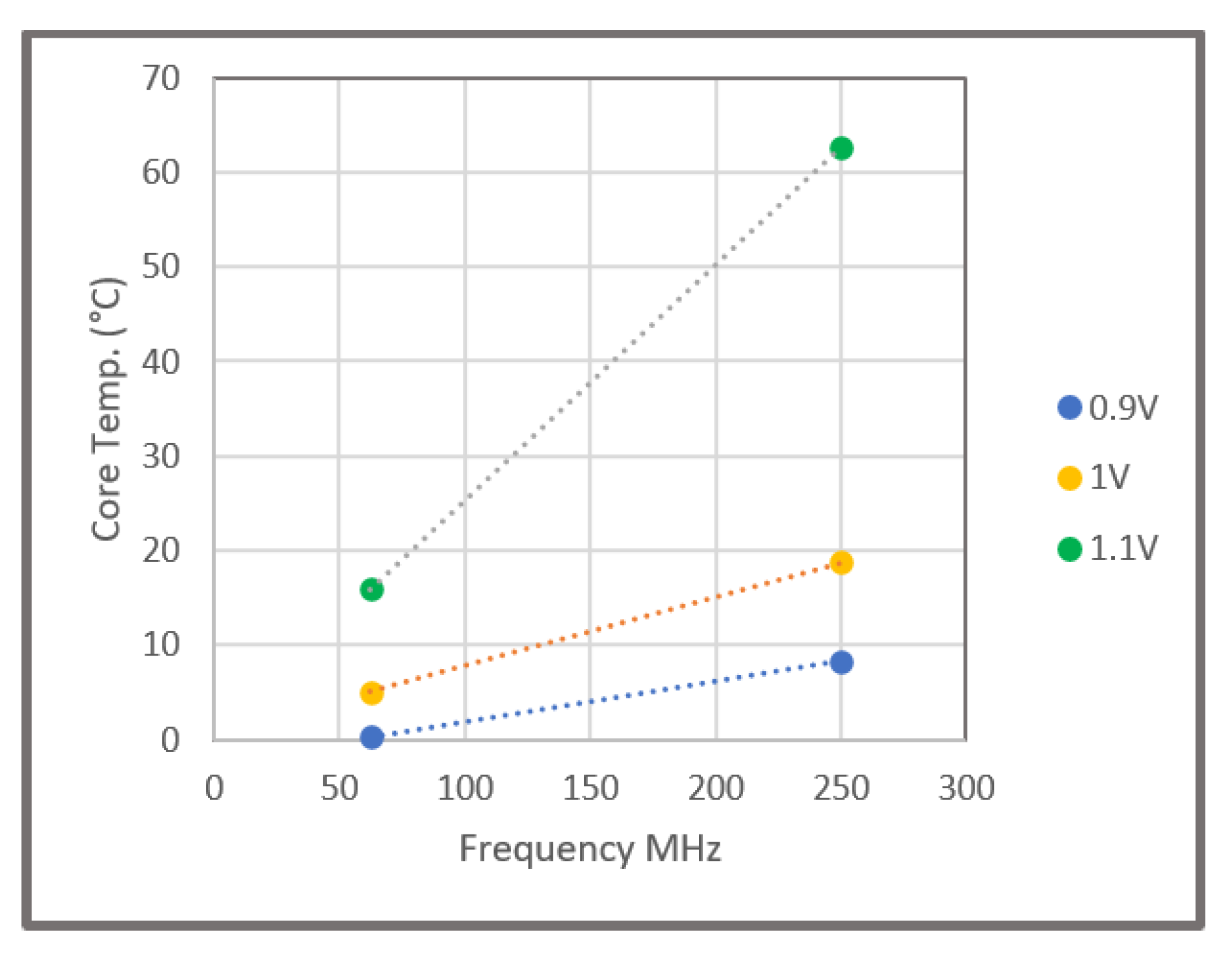
The results presented above were generated solely by use of RO circuits. The disadvantage of this techniques is that the frequency of the rings is dictated by its number of stages. Separation of the operation frequency from the ring size allows more flexibility in illustrating the power dissipation of the chip. An expansion of the study is in development to profile the system-level testing using inverter chains with an external clock. Initial results of the study, presented in Figure 4, are in line with the thermal dissipation figures mentioned above. The test used 140 inverter chains, each with 151 stages, for a total of 21,140 logic elements. The tests were performed in two frequencies: 62.5 MHz and 250 MHz and three voltages. Further details will be presented in a later study.
3. Degradation Signal Tempering Using Noise Reduction Techniques
The section above elaborates on the thermal management problem introduced in FinFET technologies. The objective of the remainder of the paper is to provide a solution for mitigating the thermal concerns in packaged devices in the field. In contrast to the testing performed in the MTOL procedure, where the stress conditions are above use conditions, this solution monitors the devices in regular use. Receiving clear degradation data in use conditions is a challenge. We demonstrate later in the study that accurate monitoring is only possible by implementing noise reduction techniques, as detailed below.
3.1. Degradation Data Correction with Temperature Compensation
A method was developed to increase the accuracy by means of compensation of frequency deviations caused by temperature change. The data were collected from MTOL tests with different ambient temperatures. The data were collected from multiple tests to find the frequency changes for different base frequencies. Although the tests used a temperature-regulated chamber, there were temperature fluctuations up to 5 degrees. The frequency variations due to temperature change were recorded. The results were normalized to show a linear change with a slope of 0.0012. Using the slope found in the data, we developed an expression for correcting the degradation pattern in any frequency, as detailed in Equation (5):
where f0 is the frequency measured, m is the slope of the frequency change due to the temperature, and the formula below represents the offset of the temperature:
meaning that 60 °C is the expected average chip temperature and T0 is the temperature measured.
The technique was used in tests in several temperature and frequency modes. Figure 5 shows an example of data corrected using the temperature compensation formula. The original data have an undiscernible signal due to the distortion of the temperature fluctuations. The second plot shows the corrected data, indicating a clear degradation signal. Since monitors are designed to operate in regular use conditions, which are prone to non-negligible temperature fluctuations, the thermal compensation procedure is critical for the use of the monitor.
3.2. Accurate Lifetime Calculations Using Early Failures
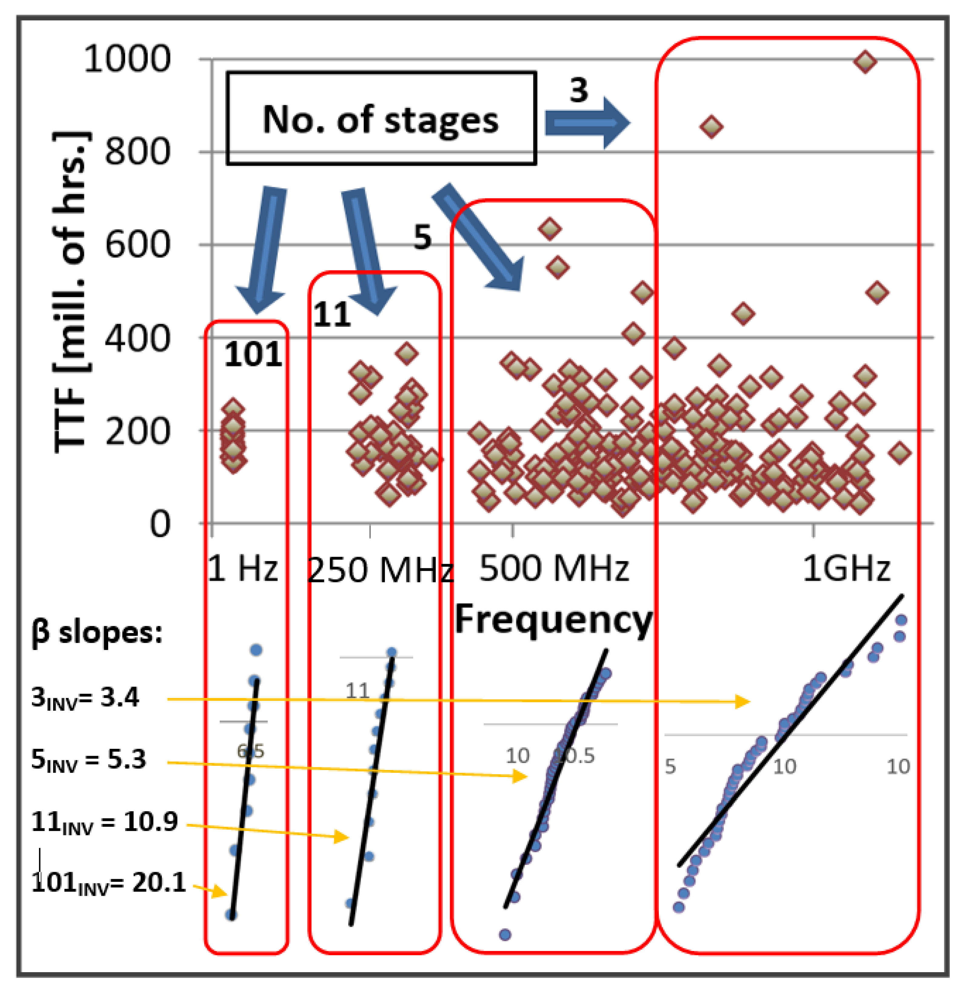
We found that temperature compensation alone did not sufficiently decease the noise in the of a microchip monitor. It was apparent that more efforts would be necessary to bring the SNR to an acceptable level. In previous studies, Weibull distributions were used to show that the amount of dispersion of the TTF values directly corresponds to the number of stages in the ring circuits [7]. When the TTF values are set to a ring frequency plot, the data in low frequencies conserve a tight pattern and fan out in the higher frequency rings. We used the Weibull distribution (shown in Equation (7)) to analyze the transition of the TTF pattern from low frequencies to high frequencies.
θ is the mean TTF and β is the shape parameter. Figure 6 is a visualization of the correlation between the amount of distribution of the TTF data to the number of stages in the rings. The data in the plot upper part of the figure are a TTF to frequency plot. An increase in dispersion with the increase in frequency is clearly observed. The lower part of the figure shows Weibull distributions that are formulated from the data in the TTF plot above them. The plot is sectioned into 4 different parts correlating to data created from rings of a uniform size. The rings have 3, 5, 11, and 101 stages. The Weibull slopes underneath are labeled with their respective β slope values. The gradient of the β slope shows the level of determinism of the failure times in a Weibull distribution. A clear one-to-one correlation between the number of stages in the rings to the β slope appears.
The trend is also developed analytically. A ring, comprised of a chain of inverters, produces an output frequency based on the transition delay of all the stages. A single stage will degrade at a random rate. Totally random elements generate a Weibull distribution with a β slope of 1. By chaining the elements together, the variance of the stages is averaged together to raise the determinability of the results corresponding to the number of stages in the ring. Comparable results are received for different stress modes and technologies. Additional explanation is provided in [7].
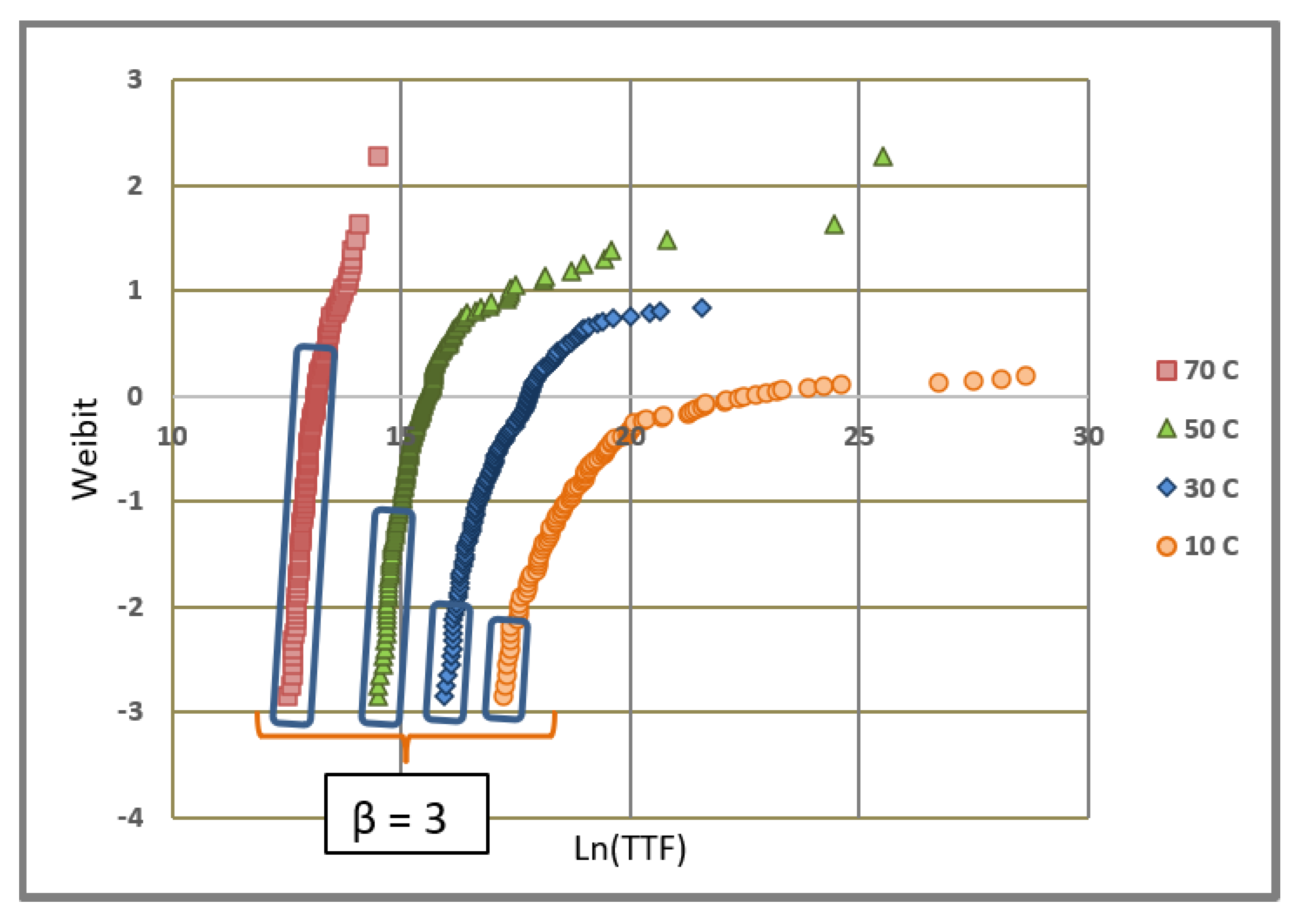
We analyzed the data of the low stress tests, as detailed in a previous study [24]. The results that we received seem to contradict the trend described above. Figure 7 displays a set of four Weibull distributions of three-stage rings tested with a nominal core voltage of 0.85 V. The single distinguishing factor between the stress conditions of the tests presented are the ambient temperatures. Each differs from the other by 20 °C: 10 °C, 30 °C, 50 °C, and 70 °C. The plots are marked with a straight dotted line to mark a β slope of 3. The 70 °C shows a characteristic Weibull distribution with the expected β slope of 3. As the temperature of the test decreases, the data veers more and more from the expected Weibull distribution trend. Since the tests are under low stress, the outcome is easily explained. The TTF is figured from the slope of frequency degradation. When the slope is too slight, the degradation signal is indiscernible from the noise of the system. Therefore, the data veering from the expected Weibull trend does not contribute information to the failure trend.
It is very important to point out that the early failure times (values starting from the bottom left side of the plots) are consistently congruent with the expected Weibull trend. We found that the Weibull slopes of the early failure data are comparable to those calculated from high stress tests. This validates the theory that the early failures are an authentic part of the signal. Basing a failure trend on the early failures is acceptable since the Weibull distribution is a weakest-link-type distribution. The early failures are a prediction of the later failures [25]. Therefore, it is sufficient to observe the early failures to see the trend of the system. The mean time-to-fail (MTTF) value or θ is the zero point of the Weibull plot. Since we have actual TTF measurements with their Weibull characteristics, each test reveals the reliability distribution function of the device for that specific stress condition.
We have demonstrated that, as the stress of the test is lowered, the noise in the results is more visible in the data. Correction of the data by excluding longer failure times is less effective with the decrease in stress. In any case, the results obtained by filtering out non-fitting parts of the plot show a high level of accuracy. The outcome shows frequency dependence, as it is seen that the TTF is shorter in the higher frequencies. The results of the tests remain well within the range of values received in tests run in high temperature, voltage, and frequency stresses in previous studies [16].
4. Algorithm to Calculate the TTF of Early Failures
From the thermal management study elaborated above, we have determined that the lifetime estimate of 16 nm FinFET technology can be characterized using a single TTF model, as defined in Equation (2). The data extracted from MTOL tests based on this model were used as a control set for comparison to TTF measurements of the devices in real time. We implemented a microchip health monitoring system into Ultra96 MPSoC development boards, based on the design plan detailed in [7], in C language. The FPGA of the system included 140 ring oscillators, all with three stages, developed using VHDL. The system calculated the TTF of the boards over aging windows of 16 h. The TTF calculation was preformed using the following formula:
where “t” is the time in hours, and “n” is the time power law for the degradation of BTI. We found that the n is about 4. α is the relative change in the frequency in the test, defined by:
“Δf” is the displacement of the ring circuit frequency due to degradation in the test. “f0” is the initial frequency of the circuit.
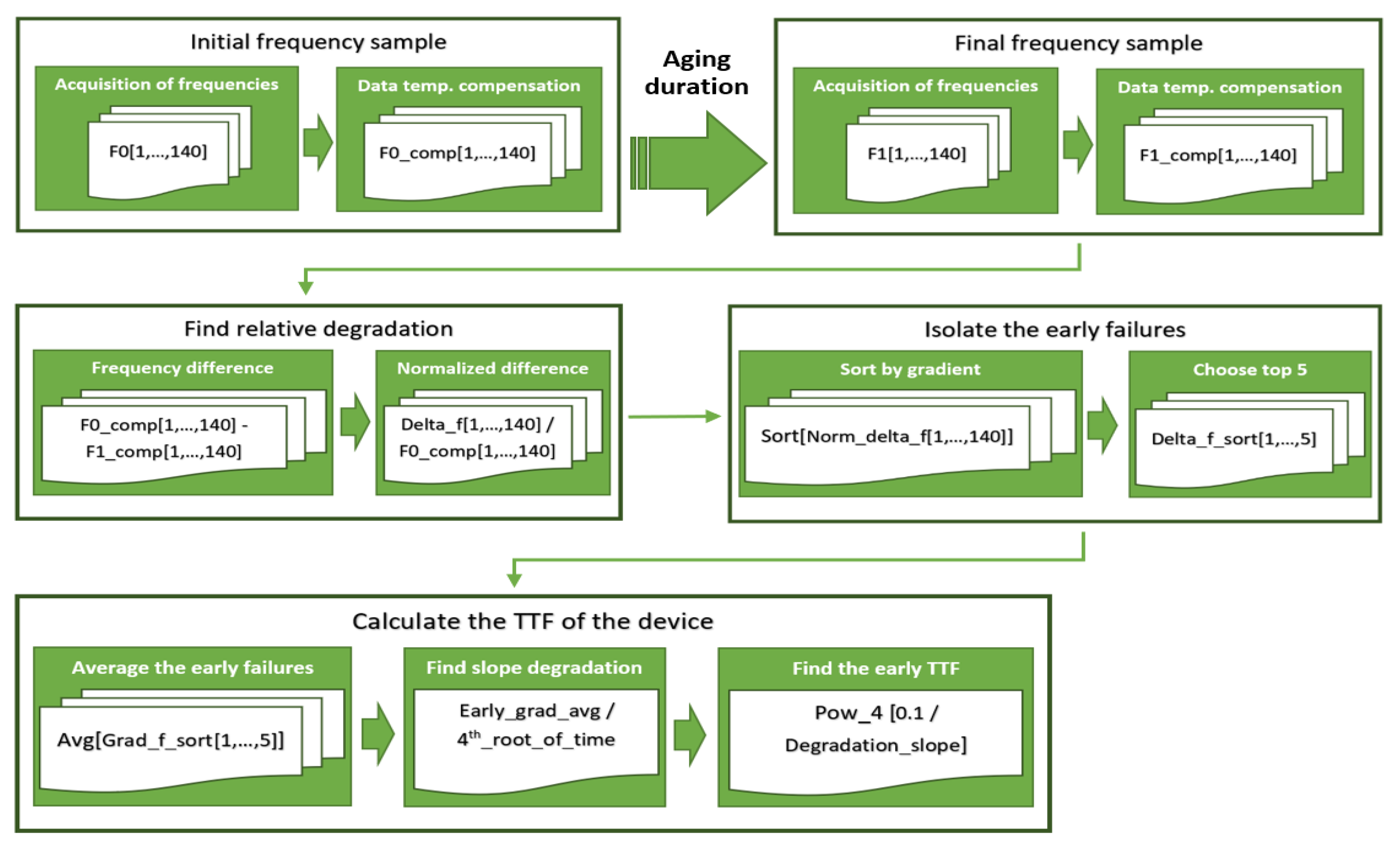
Initially, we attempted to achieve accurate TTF measurements by averaging the TTF values of the 140 rings. This is the procedure used to obtain accuracy in the tests with high stress. In this case, where devices are operating at regular use conditions, the results lacked stability and were unsatisfactory. We concluded that the measurements received were not recording the degradation of the system, but rather system noise. We then developed an algorithm that implemented the noise reduction techniques explained in Section 3. The flow of the algorithm is presented in Figure 8 below. The first two actions detailed in the first level of the flow are acquisitions of the initial and final sample frequencies of all the rings and are stored in arrays F0 and F1. The data extracted are adjusted using the temperature compensation Formulas (7) and (8), and are stored in arrays F0_comp and F1_comp. Next, the normalized displacement of each individual ring is calculated. The difference in frequencies is found by storing F0_comp–F1_comp into Delta_f and them normalizing it by dividing by F0_comp and sorting the results in Norm_delta_f. The normalized differences are sorted using the “sort” function from largest to smallest. The solution is in array Delta_f_sort. We chose the first five values from the array to obtain the early failures. These values were averaged and stored in the scalar Early_grad_avg. This value was divided by the time value, which, in our case, was simply 2 h (since the 4th root of 16 is 2) to obtain the slope degradation. The result was used to calculate the TTF of the system.
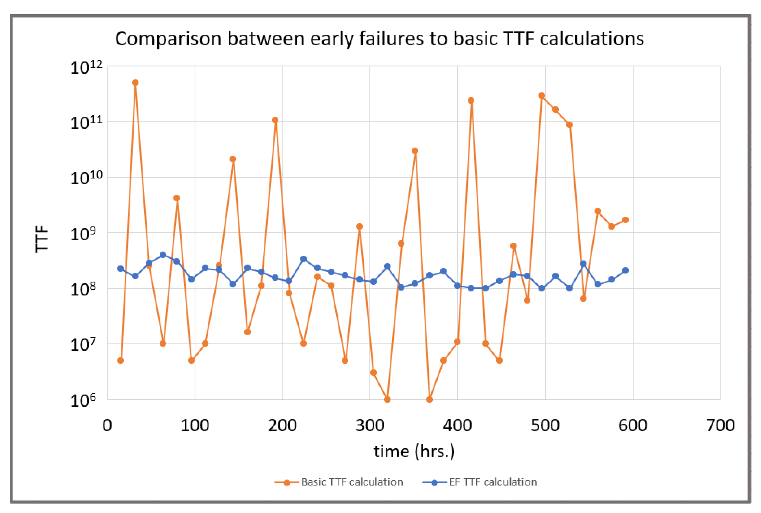
Figure 9 shows results of the MHM system calculation over about 600 h. The first plot is the measurements of the system using the original approach, which is simply averaging the TTF values. One can see that the results are very erratic. In contrast, the second plot shows the results of measurements incorporating the noise reduction techniques. The results remain stable throughout the test. The variance in the noise-reduced data is about 0.2 orders of magnitude, and for the non-optimized data it is about 6 orders of magnitude.
The system with noise reduction is an excellent self-gauge of the expected lifetime of a chip. The results of this study are significant for testing individual chips to mitigate thermal hazard occurrences. The benefit of the method is that it is far more powerful in monitoring the activity of a large system with hundreds or thousands of chips such, as in data centers. This system can be expanded to provide the information needed to choose how to allocate resources, based on a study performed previously [26]. Tasks that require heavy resources can be allocated to strong servers, and low-resource tasks to weaker servers.
5. Conclusions
We have demonstrated how the implementation of a noise-reduced microchip health sensor helps to isolate thermal management concerns in packaged 16 nm FinFET devices. The technique also reveals the upper power dissipation limits of the system due to the usage of dynamic logic. The outcome of the investigation was applied to develop a system that monitors thermal hazards in the chips in real time. Noise-reduction procedures were adopted to facilitate the use of the monitor to obtain stable results. A novel algorithm for reducing noise in TTF data is proposed and implemented in MPSoC devices. The results of the testing show a dramatic improvement in the stability of the TTF measurements, providing an excellent vehicle for chip monitoring both in small and large systems. The benefits of the study are far reaching, and further research is in progress to advance the achievement of the work.
Author Contributions
Conceptualization, J.B.B. and D.S.B.; methodology, J.B.B.; software, E.B.; validation, J.B.B. and D.S.B.; formal analysis, E.B.; investigation, E.B.; resources, J.B.B.; data curation, E.B.; writing—original draft preparation, E.B.; writing—review and editing, E.B.; visualization, D.S.B.; supervision, J.B.B.; project administration, D.S.B.; funding acquisition, J.B.B. All authors have read and agreed to the published version of the manuscript.
Funding
This research received no external funding.
Data Availability Statement
The data presented in this study are available on request from the corresponding author.
Acknowledgments
Many thanks for the ongoing support from: Ariel University Advanced Studies Research Group, Ariel Israel. Many thanks to the Microsystems Technology Laboratories research department at Massachusetts Institute of Technology for their invaluable inputs, which significantly raised the quality of this work.
Conflicts of Interest
The authors declare no conflict of interest.
References
- Sagong, H.C.; Choi, K.; Kim, J.; Jeong, T.; Choe, M.; Shim, H.; Kim, W.; Park, J.; Shin, S.; Pae, S. Modeling of FinFET Self-Heating Effects in multiple FinFET Technology Generations with implication for Transistor and Product Reliability. In Proceedings of the IEEE 2018 Symposium on VLSI Technology, Honolulu, HI, USA, 18–22 June 2018; pp. 121–122. [Google Scholar] [CrossRef]
- Myeong, I.; Son, D.; Kim, H.; Shin, H. Analysis of Self Heating Effect in DC/AC Mode in Multi-Channel GAA-Field Effect Transistor. IEEE Trans. Electron Dev. 2019, 66, 4631–4637. [Google Scholar] [CrossRef]
- Kumar, A.; Srinivas, P.S.T.N.; Tiwari, P.K. Physical Insight into Self-heating Effects in Ultrathin Junctionless Gate-All-Around FETs. In Proceedings of the 2019 IEEE 9th International Nanoelectronics Conferences (INEC), Kuching, Malaysia, 3–5 July 2019; pp. 1–4. [Google Scholar] [CrossRef]
- Liao, M.-H.; Hsieh, C.-P.; Lee, C.-C. Systematic Investigation of Self-Heating Effect on CMOS Logic Transistors From 20 to 5 nm Technology Nodes by Experimental Thermoelectric Measurements and Finite Element Modeling. IEEE Trans. Electron Dev. 2017, 64, 646–648. [Google Scholar] [CrossRef]
- Sootkaneung, W.; Howimanporn, S.; Chookaew, S. Thermal Effect on Performance, Power, and BTI Aging in FinFET-Based Designs. In Proceedings of the IEEE 2017 Euromicro Conference on Digital System Design, Vienna, Austria, 30 August–1 September 2017; pp. 345–351. [Google Scholar] [CrossRef]
- Drego, N.; Chandrakasan, A.; Boning, D. An All-Digital, Highly Scalable Architecture for Measurement of Spatial Variation in Digital Circuits. In Proceedings of the IEEE Asian Solid-State Circuits Conference, Fukuoka, Japan, 3–5 November 2008; pp. 393–396. [Google Scholar]
- Bender, E.; Bernstein, J.B. Microchip Health Monitoring System Using the FLL Circuit. Sensors 2021, 21, 2285. [Google Scholar] [CrossRef] [PubMed]
- Bernstein, J.B.; Gurfinkel, M.; Li, X.; Walters, J.; Shapira, Y.; Talmor, M. Electronic circuit reliability modeling. Microelectron. Reliab. 2006, 46, 1957–1979. [Google Scholar] [CrossRef]
- Bernstein, J.B.; Gabbay, M.; Delly, O. Reliability matrix solution to multiple mechanism prediction. Microelectron. Reliab. 2014, 54, 2951–2955. [Google Scholar] [CrossRef]
- Ultra96 Hardware User’s Guide, version 0.9; Avnet Inc.: Phoenix, AZ, USA, 2018.
- Bender, E.; Bernstein, J.B. Self-Heating Effects Measured in Fully Packaged FinFET Devices. In Proceedings of the IEEE 32nd International Conference on Microelectronics (Miel), Niš, Serbia, 12–14 September 2021. [Google Scholar]
- Jiang, H.; Liu, X.; Xu, N.; He, Y.; Du, G.; Zhang, X. An Investigation of DC/AC Hot Carrier Degradation in Multiple-fin SOI FinFETs. IEEE Electron Device Lett. 2015, 36, 1258–1260. [Google Scholar] [CrossRef]
- Paliwoda, P.; Chbili, Z.; Kerber, A.; Nigam, T.; Singh, D.; Nagahiro, K.; Manik, P.; Cimino, S.; Misra, D. Self-heating effects on Hot carrier degradation and its impact on Ring Oscillator reliability. In Proceedings of the 2018 International Integrated Reliability Workshop (IIRW), South Lake Tahoe, CA, USA, 7–11 October 2018; pp. 1–4. [Google Scholar] [CrossRef]
- Choi, J.; Monga, U.; Park, Y.; Shim, H.; Kwon, U.; Pae, S.; Kim, D. Impact of BEOL Design on Self-heating and heating and Reliability in Highly-scaled FinFETs. In Proceedings of the International Conference on Semiconductor Processes and Devices (SISPAD), Udine, Italy, 4–6 September 2019; pp. 1–4. [Google Scholar] [CrossRef]
- Kim, J.; Hong, K.; Shim, H.; Rhee, H.; Shin, H. Comparative Analysis of Hot Carrier Degradation (HCD) in 10-nm Node nMOS/pMOS FinFET Devices. IEEE Trans. Electron Dev. 2020, 67, 5396–5402. [Google Scholar] [CrossRef]
- Stellari, F.; Jenkins, K.A.; Weger, A.J.; Linder, B.; Song, P. Self-Heating Characterization of FinFET SOI Devices using 2D Time Resolved Emission Measurements. In Proceedings of the IEEE International Reliability Physics Symposium (IRPS), Monterey, CA, USA, 19–23 April 2015; pp. 2B.1.1–2B.1.6. [Google Scholar] [CrossRef]
- Bernstein, J.B.; Bensoussan, A.; Bender, E. Reliability Prediction of FinFET FPGAs by MTOL. Microelectron. Reliab. 2020, 114, 113809. [Google Scholar] [CrossRef]
- Qu, Y.; Lin, X.; Li, J.; Cheng, R.; Zheng, Z.; Lu, J.; Chen, B.; Zhao, Y. Ultra Fast (<1 ns) Electrical Characterization of Self-Heating Effect and Its Impact on Hot Carrier Injection in 14nm FinFETs. In Proceedings of the 2017 IEEE International Electron Devices Meeting (IEDM), San Francisco, CA, USA, 2–6 December 2017; pp. 39.2.1–39.2.4. [Google Scholar] [CrossRef]
- Zhang, G.; Gu, Y.; Li, J.; Tao, H. An Improved Model of Self-Heating Effects for Ultrathin Body SOI nMOSFETs Based on Phonon Scattering Analysis. IEEE Electron Device Lett. 2015, 36, 534–536. [Google Scholar] [CrossRef]
- Makovejev, S.; Olsen, S.; Raskin, J.-P. RF Extraction of Self-Heating Effects in FinFETs. IEEE Trans. Electron Dev. 2011, 53, 3335–3341. [Google Scholar] [CrossRef]
- Bernstein, J.B.; Bensoussan, A.; Bender, E. Reliability prediction with MTOL. Microelectron. Reliab. 2017, 68, 91–97. [Google Scholar] [CrossRef] [Green Version]
- UltraScale Architecture System Monitor, V1.10. AMD Xilinx. Available online: https://docs.xilinx.com/v/u/en-US/ug580-ultrascale-sysmon (accessed on 7 October 2022).
- DP800 Series Programmable Linear Power Supply; Rigol Technologies, Inc.: Beijing, China, 2015.
- Bender, E.; Bernstein, J.B. Product Failure Time Assessments using Early Degradation Filtering. Eng. Technol. Open Acc. 2021, 3, 555625. [Google Scholar] [CrossRef]
- McPheirson, M.P. Reliability and Physics Engineering; Springer: Berlin/Heidelberg, Germany, 2010. [Google Scholar] [CrossRef]
- Drego, N.; Chandrakasan, A.; Boning, D.; Shah, D. Reduction of Variation-Induced Energy Overhead in Multi-Core Processors. IEEE Trans. Comput.-Aided Des. Integr. Circuits Syst. 2011, 30, 891–904. [Google Scholar] [CrossRef]
Figure 1.
Three TTF-to-frequency plots. The TTF decreases with the increase in stress. The decrease in TTF with frequency is similar across all the tests, showing a decrease in TTF to about 75%.
Figure 1.
Three TTF-to-frequency plots. The TTF decreases with the increase in stress. The decrease in TTF with frequency is similar across all the tests, showing a decrease in TTF to about 75%.

Figure 2.
TTF plots of four stress modes plotted in four different frequencies: 30 MHz–1 GHz. The slopes of all the plots show an activation energy of 0.49 eV. V’ is e^(−Vγ). T’ is T + ΔTSHE.
Figure 2.
TTF plots of four stress modes plotted in four different frequencies: 30 MHz–1 GHz. The slopes of all the plots show an activation energy of 0.49 eV. V’ is e^(−Vγ). T’ is T + ΔTSHE.

Figure 3.
Surface plot showing the increase in core temperature due to dynamic power dissipation with an ambient temperature of 25 °C. The plot shows the temperature increase with the increase in the number of dynamic logic cells, as well as the increase in voltage.
Figure 3.
Surface plot showing the increase in core temperature due to dynamic power dissipation with an ambient temperature of 25 °C. The plot shows the temperature increase with the increase in the number of dynamic logic cells, as well as the increase in voltage.

Figure 4.
Temperature offset of the chip using open inverter chains. The results include three different core voltages: 0.9 V, 1 V, and 1.1 V.
Figure 4.
Temperature offset of the chip using open inverter chains. The results include three different core voltages: 0.9 V, 1 V, and 1.1 V.

Figure 5.
An example of degradation data before compensation (a) and after compensation (b). The stress conditions are a 45 °C ambient temperature and a core voltage of 1.1 V.
Figure 5.
An example of degradation data before compensation (a) and after compensation (b). The stress conditions are a 45 °C ambient temperature and a core voltage of 1.1 V.

Figure 6.
A TTF-to-frequency plot sectioned into four sectors defined by ring sizes of 3, 5, 11, and 101 inverters. The corresponding Weibull plots for the four sectors are displayed below the TTF values for each ring group with their β slope values.
Figure 6.
A TTF-to-frequency plot sectioned into four sectors defined by ring sizes of 3, 5, 11, and 101 inverters. The corresponding Weibull plots for the four sectors are displayed below the TTF values for each ring group with their β slope values.

Figure 7.
Weibull distributions of three-stage rings are displayed for the following four different external stress temperatures: 10, 30, 50, and 70 °C. The section that conserves a characteristic β slope of three for three-stage rings is circled.
Figure 7.
Weibull distributions of three-stage rings are displayed for the following four different external stress temperatures: 10, 30, 50, and 70 °C. The section that conserves a characteristic β slope of three for three-stage rings is circled.

Figure 8.
A diagram of the flow for implementing temperature compensation and early failure filtering into a MHM system. The techniques are performed on 140 three-stage ring oscillators.
Figure 8.
A diagram of the flow for implementing temperature compensation and early failure filtering into a MHM system. The techniques are performed on 140 three-stage ring oscillators.

Figure 9.
A comparison of measurement data between MHM testing, with noise reduction and without.


Table 1.
A table showing the relative change in TTF with frequency for three stress modes. The TTF at 1 GHz is about 75% compared to the TTF values at 30 MHz.
Table 1.
A table showing the relative change in TTF with frequency for three stress modes. The TTF at 1 GHz is about 75% compared to the TTF values at 30 MHz.
| Stress Values | TTF at 30 MHz (h) | TTF at 1 GHz (h) | Change in TTF |
|---|---|---|---|
| −15 °C, 1.02 V | 72% | ||
| 123 °C, 0.93 V | 83% | ||
| 117 °C, 1.05 V | 73% |
Publisher’s Note: MDPI stays neutral with regard to jurisdictional claims in published maps and institutional affiliations. |
© 2022 by the authors. Licensee MDPI, Basel, Switzerland. This article is an open access article distributed under the terms and conditions of the Creative Commons Attribution (CC BY) license (https://creativecommons.org/licenses/by/4.0/).
Share and Cite
MDPI and ACS Style
Bender, E.; Bernstein, J.B.; Boning, D.S. Mitigation of Thermal Stability Concerns in FinFET Devices. Electronics 2022, 11, 3305. https://doi.org/10.3390/electronics11203305
AMA Style
Bender E, Bernstein JB, Boning DS. Mitigation of Thermal Stability Concerns in FinFET Devices. Electronics. 2022; 11(20):3305. https://doi.org/10.3390/electronics11203305
Chicago/Turabian StyleBender, Emmanuel, Joseph B. Bernstein, and Duane S. Boning. 2022. "Mitigation of Thermal Stability Concerns in FinFET Devices" Electronics 11, no. 20: 3305. https://doi.org/10.3390/electronics11203305
Note that from the first issue of 2016, this journal uses article numbers instead of page numbers. See further details here.