Article

New Resistor-Less Electronically Controllable ±C Simulator Employing VCII, DVCC, and a Grounded Capacitor

1
Department of Industrial and Information Engineering (DIIIE), University of L’Aquila, 67100 L’Aquila, Italy
2
DEWS, University of L’Aquila, 67100 L’Aquila, Italy
*
Author to whom correspondence should be addressed.
Electronics 2022, 11(2), 286; https://doi.org/10.3390/electronics11020286
Submission received: 22 December 2021 / Revised: 10 January 2022 / Accepted: 13 January 2022 / Published: 17 January 2022
(This article belongs to the Section Circuit and Signal Processing)

Abstract

:
In this paper, a new realization of electronically controllable positive and negative floating capacitor multiplier (±C) is presented. The peculiarity of the presented topology is that, for the first time, it implements a floating equivalent capacitor between its two input terminals, rather than a grounded one. To achieve the best performance, we simultaneously use the advantages provided by the current conveyor and its dual circuit, the voltage conveyor. The proposed topology is resistor free and employs one dual-output second-generation voltage conveyor (VCII±) and one electronically tunable differential voltage current conveyor (E-DVCC) as active building blocks (ABBs) and a single grounded capacitor. The value of the simulated capacitor is controlled by means of a control voltage VC which is used to control the current gain between X and Z terminals of E-DVCC. The circuit is free from any matching condition. A complete non-ideal analysis by considering parasitic impedances as well as non-ideal current and voltage gains of the used ABBs is presented. The proposed circuit is designed at the transistor level in 0.18 µm and ±0.9 V supply voltage. Simulation results using the SPICE program show a multiplication factor ranging from ±10 to ±25.4 with a maximum error of 0.56%. As an example, the application of the achieved floating capacitor as a standard high pass filter is also included.

1. Introduction

The advantages of capacitance multipliers in realizing large value capacitors in the CMOS process regarding the cost and chip size reduction are well known [1,2,3,4,5,6]. Capacitance multipliers find wide use in applications requiring large time constants, such as low-frequency filters in biomedical applications. In recent years, capacitor multiplier implementation has become a more important topic and several techniques have been developed to realize capacitor multipliers [7,8,9,10,11,12,13,14,15,16,17,18,19]. The feature of electronic tuning is considered a great advantage because it gives suitable tuning of filters, oscillators, and other circuits employing the simulated capacitor. Based on the intended application, simulated capacitors can be either grounded or floating.
Literature survey shows that various active building blocks (ABBs) have been used to develop floating capacitance multipliers [7,8,9,10,11,12,13,14,15,16,17,18,19,20,21]. The used ABBs are mainly the second-generation current conveyor (CCII) [22,23], current-controlled differential difference current conveyor (CCDDCC) [24,25], current follower transconductance amplifier (CFTA) [26], voltage current gain controlled second-generation current conveyor (VGC-CCII), dual output second-generation current conveyor (Do-CCII) [27], current-controlled second-generation current conveyor (CCCII), differential voltage current conveyor (DVCC), multiple output DVCC(MODVCC), differential voltage current conveyor transconductance amplifier (DVCCTA), operational transconductance amplifier (OTA), and flipped voltage follower (FVF) [28]. However, the previous implementations of floating capacitors in [7,8,9,10,11,12,13,14,15,16,17,18,19] suffer from several drawbacks. For example, the circuit reported in [7] employs two OTA, one CCII, and one resistor, and the achieved floating capacitor shows a high error. The power consumption of the circuits reported in [9,11,12,13,17] is high. The solution reported in [9] uses five CFTA and the one reported in [19] requires four OTA. The circuits reported in [12,13,15,17,18,20,21] lack electronic tuning capability. In the circuits reported in [10,14,17,18,21], a floating capacitor is employed. More importantly, in [17], two floating capacitors are used which must be well matched. Even worse, in [18], four floating capacitors are used, and matching is required between these four capacitors.
Recently, the application of a second-generation voltage conveyor (VCII) [29,30,31] as the dual circuit of CCII has been investigated in realizing impedance simulators [2,32,33,34]. In particular, in [2,33], its application in simulating grounded capacitor multiplier is shown, where the VCII-based grounded capacitors outperform the previously reported works in many terms.
In this paper, we intend to use the intrinsic capabilities of VCII in designing high-performance floating capacitor multipliers. To this aim, we introduce a new topology to implement a floating capacitor using a dual output VCII, an electronically controllable DVCC (which we call E-DVCC), and a grounded capacitor. In order to have an electronic tuning capability, the current gain between the X and Z terminals of E-DVCC is controlled using a control voltage, VC. Employing both VCII and DVCC in the proposed topology, the benefits of voltage conveyors and current conveyors are combined to achieve the desired properties of floating capacitance multiplication, low-voltage low-power operations, reduced associated parasitic elements, electronic tunability, low error, no matching condition, and simple circuitry. Both positive and negative multiplications can be implemented by the proposed circuit. A complete non-ideal analysis is given, and the SPICE simulation results are reported. The application of the proposed floating capacitor as a standard high pass filter is also given, as an application of study.
The organization of this paper is as follows: in Section 2, the proposed circuit is introduced; in Section 3, non-ideal analysis is performed; Section 4 shows the implementation of the active blocks; Section 5 includes the simulation results; and finally, Section 6 concludes the paper.

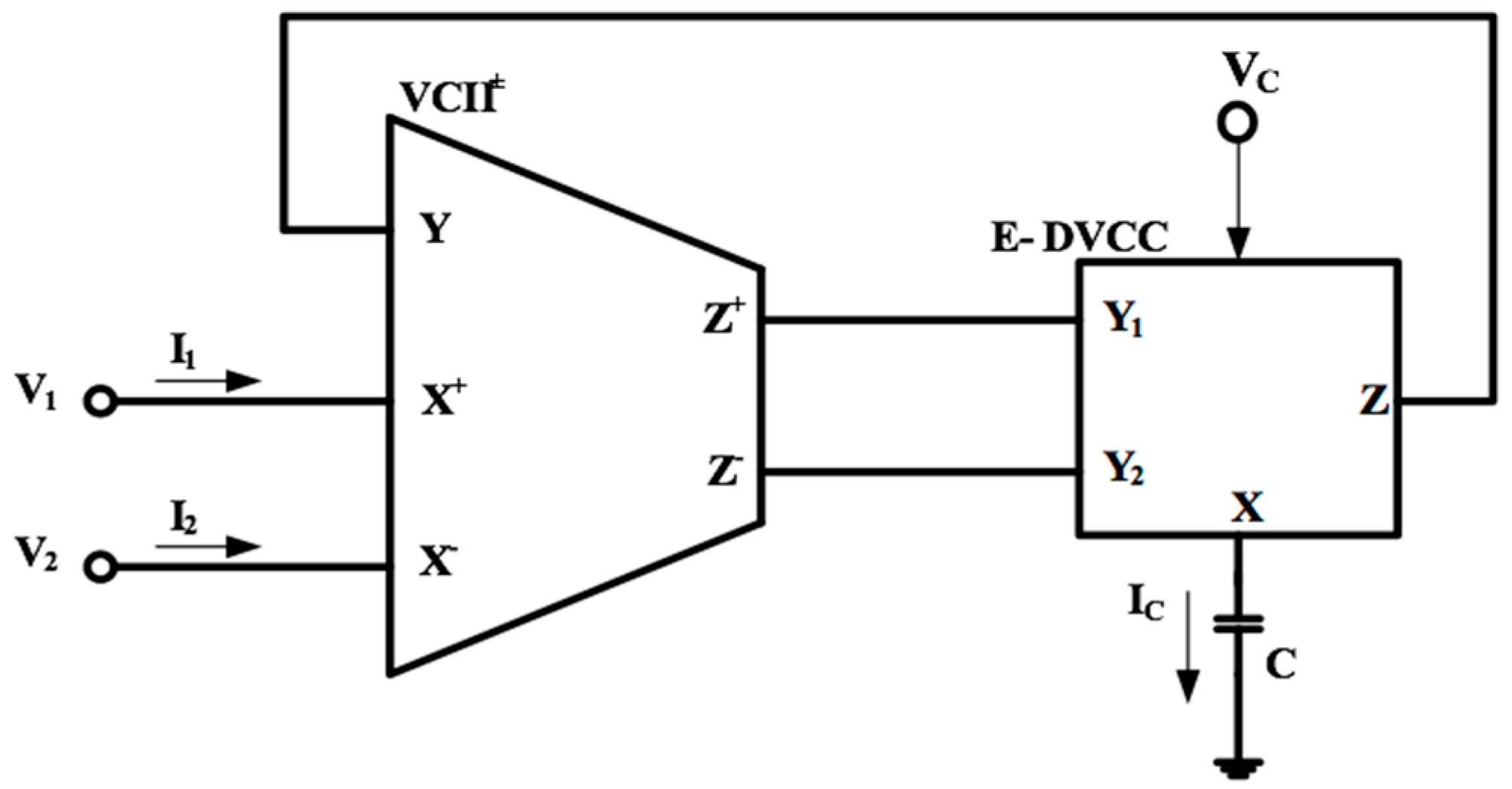
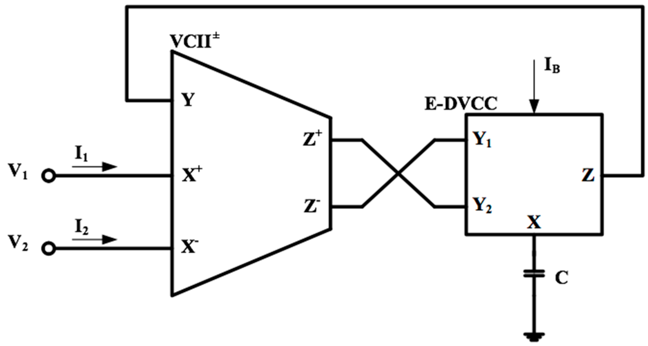
2. The Proposed VCII-Based Floating ±C Multiplier

The proposed VCII-based floating +C multiplier is shown in Figure 1. It is composed of one VCII±, one E-DVCC, and a single grounded capacitor. Here, we use the intrinsic potential of voltage conveyors and current conveyors to achieve a high-performance floating capacitor multiplier. In the E-DVCC, the current gain between the X and Z terminals can be regulated by the voltage VC which allows us to electronically control the value of simulated +C. Consequently, as it will be shown, the value of the simulated floating capacitor can be varied by VC.
In the following, we perform the analysis of the proposed circuit: operation the VCII± is ideally expressed by the equations:
I X + I X V Z + V Z V Y = 1 0 0 0 1 0 0 0 0 1 0 0 0 0 1 0 0 0 0 0 I Y V X + V X I Z
while the following matrix represents the ideal operation of E-DVCC:
V X I Y 1 I Y 2 I Z = 1 1 0 0 0 0 0 0 0 0 0 0 0 0 K 0 V Y 1 V Y 2 I X V Z
Being K, the tunable current gain between the X and Z terminals. Using Equation (3a,b) for VZ+ and VZ− we have:
VZ+ = V1,
VZ = V2,
where V1 and V2 are the input voltages. Using (2) and (3a,b) the voltage across C is:
VX = VY1VY2 = V1V2
From Equation (4), the produced current across C is found as:
IC = sCVX = sC(V1V2)
The current produced across C is conveyed to the E-DVCC Z terminal while it is amplified by the gain of K as follows:
IZ = KIC = sKC(V1V2)
As the Z terminal of E-DVCC is directly connected to the Y terminal of VCII±, we have IY = IZ. According to Equation (1), the current at Y terminal of VCII± is conveyed to the X+ and X− terminals by gains of (+1) and (−1), respectively, so for I1 and I2 we have:
I1 = IX+ = sKC(V1V2)
I2 = IX = −sKC(V1V2)
From Equation (7a,b), the input impedance is found as:
Zin = 1/sKC
From which the equivalent capacitor is ideally:
Ceq = KC
Figure 2 shows the realization of a floating negative capacitance simulator where, differently from Figure 1, Z+ and Z− terminals of VCII± are respectively connected to Y2 and Y1 terminals of the E-DVCC. For Figure 2, it can be easily shown that the equivalent floating capacitor is ideally given
Ceq = −KC

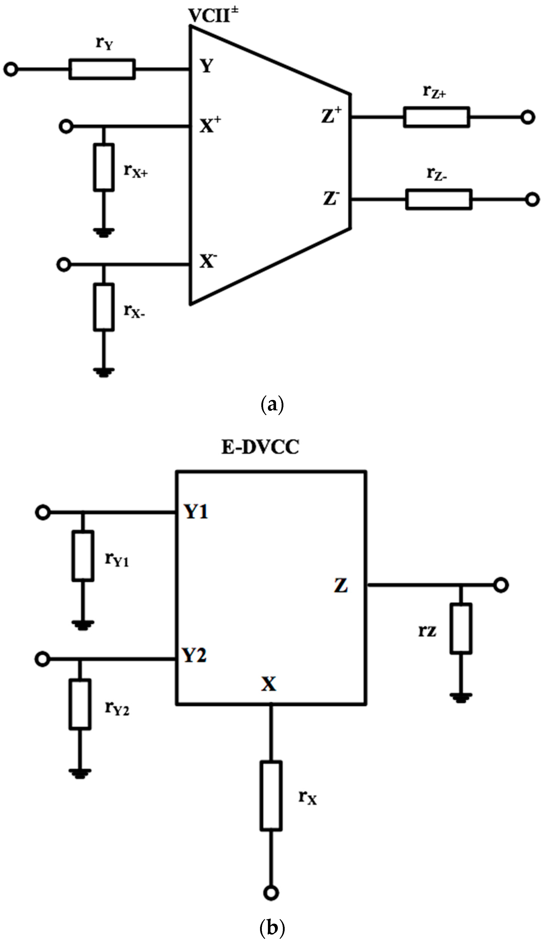
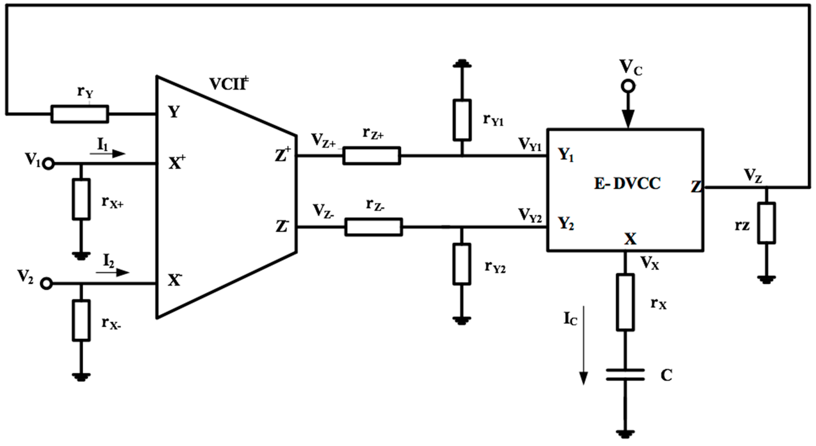
3. Non-Ideal Analysis

Figure 3 shows a more detailed representation of the used ABBs showing the parasitic impedances associated with each port of VCII± and E-DVCC. In non-ideal conditions, by considering these non-idealities, the operation of VCII± is expressed by the following matrix:
I X + I X V Z + V Z V Y = β v 1 1 r X + 0 0 β v 2 0 1 r X 0 0 α v 1 0 r Z + 0 0 α v 2 r Z r Y 0 0 0 I Y V X + V X I Z
where βv1 and βv2 are current gains between the Y and X+ terminals and between the Y and X− terminals, respectively, αv1 and αv2 are voltage gains between the X+ and Z+ terminals and between the X− and Z− terminals, respectively, with ideal values of unity. Parameters rY, rX+, rX, rZ+, and rZ− are the low-frequency impedances at the Y, X+, X−, Z+, and Z− terminals, respectively. The ideal values of rY, rX+, rX, rZ+, and rZ are zero, infinite, infinite, zero, and zero, respectively. Matrix Equation (12) represents the real operation of E-DVCC:
V X I Y 1 I Y 2 I Z = α c 1 α c 2 r X 0 0 0 0 0 0 0 0 0 0 0 K 1 r Z V Y 1 V Y 2 I X V Z
where αc1 is voltage gain between the Y1 and X terminals and αc2 is voltage gain between Y2 and X terminals, K is tunable current gain between the X and Z terminals, and rx and rz are low-frequency parasitic impedances at the X and Z terminals, respectively. The ideal value of αc1, αc2, rx, and rz are unity, unity, zero, and infinite, respectively.
Figure 4 shows the proposed positive floating C simulator while all low-frequency parasitic impedances are considered.
In Figure 4, for VZ+ and VZ we have:
V Z + = α v 1 V 1
V Z = α v 2 V 2
Using Equation (13) and considering the fact that rY1 >> rZ+ and rY2 >> rZ, for VY1 and VY2 we have:
V Y 1 = r Y 1 r Z + + r Y 1 V Z + α v 1 V 1
V Y 2 = r Y 2 r Z + r Y 2 V Z α v 2 V 2
Using Equations (12)–(14), IC is found as:
I C = s C 1 + s C r X α c 1 α v 1 V 1 α c 2 α v 2 V 2
Assuming rY << rZ, using Equations (12) and (15) we have:
I Y = s C K 1 + s C r X α c 1 α v 1 V 1 α c 2 α v 2 V 2
According to Equation (11), neglecting the parasitic components (that is 1/rx± ≅ 0), the current at Y terminal of VCII± is conveyed to the X+ and X− terminals by gains of (v1) and (−βv2), respectively, and for I1 and I2 we have:
I 1 = I X + = β v 1 I Y = s C K 1 + s C r X α c 1 α v 1 V 1 α c 2 α v 2 V 2 β v 1
I 2 = I X = β v 2 I Y = s C K 1 + s C r X α c 1 α v 1 V 1 α c 2 α v 2 V 2 β v 2
In the worst case, βv1 and βv2 can be expressed as the following where ε << 1:
β v 1 = 1 ± ε
β v 2 = 1 ε
Inserting Equation (18a) into Equation (17a) and Equation (18b) into Equation (17b) gives:
I 1 = s C K 1 + s C r X α c 1 α v 1 V 1 α c 2 α v 2 V 2 ± s C K 1 + s C r X α c 1 α v 1 V 1 α c 2 α v 2 V 2 ε
I 2 = s C K 1 + s C r X α c 1 α v 1 V 1 α c 2 α v 2 V 2 s C K 1 + s C r X α c 1 α v 1 V 1 α c 2 α v 2 V 2 ε
Using Equation (19), the input admittance of the proposed circuit is found as:
Z i n = V 1 V 2 1 + s C r X s C K α c 1 α v 1 V 1 α c 2 α v 2 V 2 ± s C K α c 1 α v 1 V 1 α c 2 α v 2 V 2 ε
The parameters αc1, αc2, αv1, and αv2 can be defined as Equation (21a–d) in which εc << 1 and εv << 1:
α c 1 = 1 ± ε c
α c 2 = 1 ε c
α v 1 = 1 ± ε v
α v 2 = 1 ε v
Inserting Equation (21a–d) into Equation (20) and simplifying the equation gives:
Z i n = 1 + s C r X s C K 1 ± ε c ± ε v = 1 s C K 1 ± ε c ± ε v + r X K 1 ± ε c ± ε v
From Equation (22), the value of Ceq is found as:
C e q = C K 1 ± ε c ± ε v
As can be seen, the non-ideal gains have a negligible effect on the value of Ceq, and in addition, using K, the value of Ceq is adjustable.
The value of the series of the parasitic capacitance of the simulated capacitor is found as:
R s e r i = r X K 1 ± ε c ± ε v
As can be seen from Equation (24), the value of Rseri is reduced by increasing multiplication factor K. The equivalent circuit of the proposed capacitor multiplier is shown in Figure 5 where Ceq is the proposed electronically tunable equivalent floating capacitance. r is the parasitic parallel resistances of the X± terminals, and Rseri is the parasitic series resistance of the simulated capacitor. A similar analysis can be performed for negative floating C.

4. The CMOS Implementation of VCII± and E-DVCC

A realization of the internal structure of VCII± is shown in Figure 6. The low impedance at the Y port is provided by the negative feedback loop made by the M1–M5 transistors. The input current to the Y port is transferred to the X+ port by a simple current mirror M6–M7. The voltage produced at the X+ node is transferred to the Z+ port by voltage buffer made by M8–M12. Similarly, the Y port input current is reversed by the current mirror, M14–M15, and transferred to the X− port. The voltage at the X− port is transferred to the Z port by M16–M20. The transistor-level implementation of an electronically tunable E-DVCC is shown in Figure 7. The difference between input voltages V1 and V2 is produced at low impedance X port utilizing the negative feedback loop established by differential pairs, M1–M2 and M3–M4, along with M5–M7 transistors as reported in [27]. In the previously reported works, DVCC is used while the gain between the X and Z terminals is unity. Here, we add a gain cell between the X and Z terminals to electronically tune the current at the Z terminal. The used gain cell is a variable gain current mirror previously reported in [35].
The current of the X terminal is transferred to the gain cell using the current mirror made of M7–M7C and M8–M8C. As was described in [35], the current gain between the X and a Z terminal is tunable by control voltage VC, expressed as:
K = I Z I X = g m 7 g m 8 1 + g m 8 r d s M 8 c 1 + g m 7 r d s M 7 c
being:
r d s M 8 c = 1 µ C o x W M 8 c L M 8 c V d d V c V T H P
and
r d s M 7 c = 1 µ C o x W M 7 c L M c V d d V T H P
where, according to the usual meaning of symbols, gmi and rdsi represent the transconductance and the drain-source resistance of the ith transistor, respectively, µ is the mobility of the carriers, Cox represents the capacitance per unit of area of the specific fabrication technology, W/Li is the ratio between the width and the length of the ith transistor, and VTH is the threshold voltage that is a technology-dependent parameter.
As it is seen from (26a), the current gain is controllable by VC.

5. Simulation Results

The proposed floating capacitor of Figure 1 is simulated in 0.18 µm CMOS technology and supply voltage of ±0.9 V using the SPICE program. The used aspect ratios are reported in Table 1. All current sources are implemented by simple current mirrors with aspect ratio of W = 9 µm and L = 0.72 µm with the values of IB1 = IB2 = IB3 = 30 µA, IB4 = 31.4 µA. The performance parameters of VCII and E-DVCC are reported in Table 2.
The value of C is set at 10 pF. To verify the functionality of the proposed circuit, the plot of impedance magnitude and phase response of the simulated floating capacitor and the ideal one are shown in Figure 8. By changing the value of VC from −0.9 V to 0 V, different multiplication factors are set. The frequency operation range of the proposed circuit results is equal to about two decades (from 10 kHz to 1 MHz). The maximum error value for different control voltages is shown in Table 3. As can be seen, the maximum error value is only 0.56%. The application of the proposed floating capacitor as a high pass filter is shown in Figure 9. The frequency response of the high pass filter for different control voltages is shown in Figure 10. The −3 dB frequencies of the filter are 100 kHz, 130 kHz, and 230 kHz for VC = −0.9 V, −0.45 V, and 0 V, respectively.
In order to examine the time domain response of the proposed circuit, an input voltage with a peak-to-peak value of 0.4 V and frequency of 1 MHz is applied. For different values of control voltages of 0, −0.45 V, and −0.9 V, the value of the input current phase is −101°, −101.4°, and −101°, respectively. The time domain responses are shown in Figure 11.
A comparison between the proposed circuit and other previously reported ones is presented in Table 4. As can be seen, the proposed circuit outperforms previous works in terms of reduced supply voltage, resistor-free structure, electronic tunability, reduced error, and simplicity.

6. Conclusions

In this paper, we present a new resistor-free topology for implementing either a positive or negative floating capacitor multiplier with electronic tuning capability. One VCII±, one E-DVCC, and a single grounded capacitor are used. Using an electronically tunable current gain stage between the X and Z terminals of the E-DVCC, various multiplication factors are achieved. The circuit enjoys low voltage operation and offers reduced error compared with other works. A non-ideal analysis is given by taking into account non-ideal gains and parasitic impedances of the used active elements. The proposed circuit is free from any restricting matching requirements. The application of the proposed circuit as a standard high pass filter is also given to verify its functionality.

Author Contributions

Editing, L.S., G.F. and V.S.; visualization, G.B., M.S. and L.S.; supervision, G.F. and V.S.; project administration, G.F. and V.S.; funding acquisition, G.F. and V.S. All authors have read and agreed to the published version of the manuscript.

Funding

This research has been partially funded by the European co-funded innovation project iRel4.0 ECSEL under grant agreement No. 876659.

Institutional Review Board Statement

Not applicable.

Informed Consent Statement

Not applicable.

Data Availability Statement

Data sharing not applicable. No new data were created or analyzed in this study. Data sharing is not applicable to this article.

Conflicts of Interest

The authors declare no conflict of interest.

References

  1. Al-Absi, M.A.; Al-Suhaibani, E.S.; Abuelma’atti, M.T. A New Compact CMOS C-Multiplier. Analog Integr. Circuits Signal Process. 2017, 90, 653–658. [Google Scholar] [CrossRef]
  2. Stornelli, V.; Safari, L.; Barile, G.; Ferri, G. A New Extremely Low Power Temperature Insensitive Electronically Tunable VCII-Based Grounded Capacitance Multiplier. IEEE Trans. Circuits Syst. II Express Briefs 2021, 68, 72–76. [Google Scholar] [CrossRef]
  3. Pennisi, S. High Accuracy CMOS Capacitance Multiplier. In Proceedings of the 9th International Conference on Electronics, Circuits and Systems, Dubrovnik, Croatia, 15–18 September 2002; Volume 1, pp. 389–392. [Google Scholar]
  4. Abuelma’atti, M.T.; Tasadduq, N.A. Electronically Tunable Capacitance Multiplier and Frequency-Dependent Negative-Resistance Simulator Using the Current-Controlled Current Conveyor. Microelectron. J. 1999, 30, 869–873. [Google Scholar] [CrossRef]
  5. Myderrizi, I.; Zeki, A. Electronically Tunable DXCCII-Based Grounded Capacitance Multiplier. AEU Int. J. Electron. Commun. 2014, 68, 899–906. [Google Scholar] [CrossRef]
  6. Shu, K.; Sanchez-Sinencio, E.; Silva-Martinez, J.; Embabi, S.H.K. A 2.4-GHz Monolithic Fractional-N Frequency Synthesizer with Robust Phase-Switching Prescaler and Loop Capacitance Multiplier. IEEE J. Solid-State Circuits 2003, 38, 866–874. [Google Scholar] [CrossRef] [Green Version]
  7. Al-Absi, M.A.; Abulema’atti, M.T. A Tunable Floating Impedance Multiplier. Arab. J. Sci. Eng. 2019, 44, 7085–7089. [Google Scholar] [CrossRef]
  8. Prommee, P.; Somdunyakanok, M. CMOS-Based Current-Controlled DDCC and Its Applications to Capacitance Multiplier and Universal Filter. AEU Int. J. Electron. Commun. 2011, 65, 1–8. [Google Scholar] [CrossRef]
  9. Li, Y. A Series of New Circuits Based on CFTAs. AEU Int. J. Electron. Commun. 2012, 66, 587–592. [Google Scholar] [CrossRef]
  10. De Marcellis, A.; Ferri, G.; Guerrini, N.C.; Scotti, G.; Stornelli, V.; Trifiletti, A. A Novel Low-Voltage Low-Power Fully Differential Voltage and Current Gained CCII for Floating Impedance Simulations. Microelectron. J. 2009, 40, 20–25. [Google Scholar] [CrossRef]
  11. Yuce, E.; Minaei, S.; Cicekoglu, O. Resistorless Floating Immittance Function Simulators Employing Current Controlled Conveyors and a Grounded Capacitor. Electr. Eng. 2006, 88, 519–525. [Google Scholar] [CrossRef]
  12. Yuce, E. A Novel Floating Simulation Topology Composed of Only Grounded Passive Components. Int. J. Electron. 2010, 97, 249–262. [Google Scholar] [CrossRef]
  13. Alpaslan, H. DVCC-Based Floating Capacitance Multiplier Design. Turk. J. Electr. Eng. Comput. Sci. 2017, 25, 1334–1345. [Google Scholar] [CrossRef]
  14. Al-Absi, M.A.; Al-Khulaifi, A.A. A New Floating and Tunable Capacitance Multiplier with Large Multiplication Factor. IEEE Access 2019, 7, 120076–120081. [Google Scholar] [CrossRef]
  15. Ananda Mohan, P.V. Floating Capacitance Simulation Using Current Conveyors. J. Circuits Syst. Comput. 2005, 14, 123–128. [Google Scholar] [CrossRef]
  16. Padilla-Cantoya, I.; Furth, P.M. Enhanced Grounded Capacitor Multiplier and Its Floating Implementation for Analog Filters. IEEE Trans. Circuits Syst. II Express Briefs 2015, 62, 962–966. [Google Scholar] [CrossRef]
  17. Tangsrirat, W. Floating Simulator with a Single DVCCTA. Indian J. Eng. Mater. Sci. 2013, 20, 79–86. [Google Scholar]
  18. Padilla-Cantoya, I. Low-Power High Parallel Load Resistance Current-Mode Grounded and Floating Capacitor Multiplier. IEEE Trans. Circuits Syst. II Express Briefs 2013, 60, 16–20. [Google Scholar] [CrossRef]
  19. Jaikla, W.; Siripruchyanan, M. An Electronically Controllable Capacitance Multiplier with Temperature Compensation. In Proceedings of the 2006 International Symposium on Communications and Information Technologies, Bangkok, Thailand, 18–20 October 2006; pp. 356–359. [Google Scholar]
  20. Kartci, A.; Ayten, U.E.; Herencsar, N.; Sotner, R.; Jerabek, J.; Vrba, K. Application Possibilities of VDCC in General Floating Element Simulator Circuit. In Proceedings of the 2015 European Conference on Circuit Theory and Design (ECCTD), Trondheim, Norway, 24–26 August 2015; pp. 1–4. [Google Scholar]
  21. Matsumoto, F.; Nishioka, S.; Ohbuchi, T.; Fujii, T. Design of a Symmetry-Type Floating Impedance Scaling Circuits for a Fully Differential Filter. Analog Integr. Circuits Signal Process. 2015, 85, 253–261. [Google Scholar] [CrossRef] [Green Version]
  22. Sedra, A.; Smith, K. A Second-Generation Current Conveyor and Its Applications. IEEE Trans. Circuit Theory 1970, 17, 132–134. [Google Scholar] [CrossRef]
  23. Alzaher, H.A.; Elwan, H.; Ismail, M. A CMOS Fully Balanced Second-Generation Current Conveyor. IEEE Trans. Circuits Syst. II Analog Digit. Signal Process. 2003, 50, 278–287. [Google Scholar] [CrossRef]
  24. Prommee, P.; Somdunyakanok, M.; Toomsawasdi, S. CMOS-Based Current-Controlled DDCC and Its Applications. In Proceedings of the 2010 IEEE International Symposium on Circuits and Systems, Paris, France, 30 May–2 June 2010; pp. 1045–1048. [Google Scholar]
  25. Torteanchai, U.; Kumngern, M.; Dejhan, K. Current-Controlled CCDDCC with Controlled Current Gain. In Proceedings of the 2011 IEEE International Conference on Computer Science and Automation Engineering, Shanghai, China, 10–12 June 2011; Volume 4, pp. 568–571. [Google Scholar]
  26. Herencsar, N.; Koton, J.; Vrba, K.; Lattenberg, I. Current Follower Transconductance Amplifier (CFTA)—A Useful Building Block for Analog Signal Processing. J. Act. Passiv. Electron. Devices 2011, 6, 217–229. [Google Scholar]
  27. Yuce, E. DO-CCII/DO-DVCC Based Electronically Fine Tunable Quadrature Oscillators. J. Circuits Syst. Comput. 2017, 26, 1750025. [Google Scholar] [CrossRef]
  28. Carvajal, R.G.; Ramirez-Angulo, J.; Lopez-Martin, A.J.; Torralba, A.; Galan, J.A.G.; Carlosena, A.; Chavero, F.M. The Flipped Voltage Follower: A Useful Cell for Low-Voltage Low-Power Circuit Design. IEEE Trans. Circuits Syst. I Regul. Pap. 2005, 52, 1276–1291. [Google Scholar] [CrossRef]
  29. Čajka, J.; Vrba, K. The Voltage Conveyor May Have in Fact Found Its Way into Circuit Theory. AEU Int. J. Electron. Commun. 2004, 58, 244–248. [Google Scholar] [CrossRef]
  30. Safari, L.; Barile, G.; Stornelli, V.; Ferri, G. An Overview on the Second Generation Voltage Conveyor: Features, Design and Applications. IEEE Trans. Circuits Syst. II Express Briefs 2019, 66, 547–551. [Google Scholar] [CrossRef]
  31. Safari, L.; Barile, G.; Ferri, G.; Stornelli, V. High Performance Voltage Output Filter Realizations Using Second Generation Voltage Conveyor. Int. J. RF Microw. Comput. Aided Eng. 2018, 28, e21534. [Google Scholar] [CrossRef]
  32. Safari, L.; Yuce, E.; Minaei, S.; Ferri, G.; Stornelli, V. A Second-Generation Voltage Conveyor (VCII)–Based Simulated Grounded Inductor. Int. J. Circuit Theory Appl. 2020, 48, 1180–1193. [Google Scholar] [CrossRef]
  33. Stornelli, V.; Safari, L.; Barile, G.; Ferri, G. A New VCII Based Grounded Positive/Negative Capacitance Multiplier. AEU Int. J. Electron. Commun. 2021, 137, 153793. [Google Scholar] [CrossRef]
  34. Yuce, E.; Safari, L.; Minaei, S.; Ferri, G.; Barile, G.; Stornelli, V. A New Simulated Inductor with Reduced Series Resistor Using a Single VCII±. Electronics 2021, 10, 1693. [Google Scholar] [CrossRef]
  35. Safari, L.; Minaei, S. A Novel Resistor-Free Electronically Adjustable Current-Mode Instrumentation Amplifier. Circuits Syst. Signal Process. 2013, 32, 1025–1038. [Google Scholar] [CrossRef]
Figure 1. The proposed floating positive capacitance multiplier.
Electronics 11 00286 g001
Figure 2. The proposed floating negative capacitance multiplier.
Electronics 11 00286 g002
Figure 3. Non-ideal impedances of (a) VCII± and (b) E-DVCC.
Electronics 11 00286 g003
Figure 4. Proposed positive floating capacitor simulator with parasitic impedances.
Electronics 11 00286 g004
Figure 5. The equivalent circuit of the proposed floating C multiplier.
Electronics 11 00286 g005
Figure 6. CMOS implementation of VCII±.
Electronics 11 00286 g006
Figure 7. CMOS implementation of E-DVCC.
Electronics 11 00286 g007
Figure 8. Frequency response of magnitude (blue) and phase (red) for the proposed (a) positive and (b) negative floating capacitor simulator.
Electronics 11 00286 g008
Figure 9. Application of the proposed simulated floating C as a high pass filter.
Electronics 11 00286 g009
Figure 10. Frequency response of the high pass filter.
Electronics 11 00286 g010
Figure 11. Time domain response of the proposed circuit (a) VC = −0.9 V (b) VC = −0.45 V, and (c) VC = 0 V.
Electronics 11 00286 g011
Table 1. The used transistors aspect ratios.
E-DVCCTransistorM1–M4M5–M6, M7, M8C, M10C, M9M7C, M9CM11, M12M8, M10
Aspect Ratio (W/L)9 µm/0.18 µm72 µm/0.9 µm7.2 µm/0.9 µm9 µm/0.9 µm720 µm/0.9 µm
VCIITransistorM1–M2, M8–M9, M17–M18, M6–M7, M13M3–M4, M10–M11, M18–M19M5, M12, M20
Aspect Ratio (W/L)9 µm/0.72 µm36 µm/0.72 µm8 µm/0.72 µm
Table 2. The simulated low-frequency characteristics of VCII± and E-DVCC.
VCII±E-DVCC
rY38.6 Ωαc10.998
rX+147.5 kΩαc20.997
rX133.7 kΩrx574 Ω
rZ+37 ΩrY1, rY2>2 GΩ
rZVC = 0 V120 kΩ
VC = −0.45 V80 kΩ
VC = −0.9 V50 kΩ
rZ−37 ΩKVC = 0 V10
β1 (DC)1.023VC = −0.45 V19.5
β2 (DC)1.01VC = −0.9 V25.4
αv1 (DC)0.983PdVC = 0 V1.43 mW
αv2 (DC)0.983VC = 0 V2.03 mW
Pd0.804 mWVC = −0.9 V2.38 mW
Table 3. Deviation between theoretical and simulated values at different multiplication factors, C = 10 pF and f = 100 kHz.
VCMultiplication FactorExpected Value of CeqSimulated
Value of Ceq
% Error
Positive simulatorVC = 0 V10100 pF99.4 pF−0.6
VC = −0.45 V19.5195 pF196.1 pF0.56
VC = −0.9 V25.4254 pF255.4 pF0.55
Negative simulatorVC = 0 V10−100 pF−99.47 pF−0.53
VC = −0.45 V19.5−195 pF−196 pF0.51
VC = −0.9 V25.4−254 pF−255.3 pF0.51
Table 4. Comparison between proposed circuit and other reported works.
Electronic TuningMax ErrorVdd–VssPower ConsumptionNumber of TransistorsPassive ElementsABBRef
RFloating C
Yes20% 1NANANA1No2OTA + CCII[7]
YesNA±1.25 V4.05 Mw 2990No3CCDDC[8]
YesNA±1.5 VNA1040No4CFTA[9]
YesNA2 V0.7 mW470YesVGC-CCII[10]
YesNA±2.5 V4.98 mW700NoDo-CCII + 3CCCII[11]
NoNA±1.5 V9.52 mW362No2DVCC[12]
NoNA±0.75 V1.29 mW982No2MODVCC[13]
Yes8.60%±0.75 V2.3 µW–6.34 µW760YesCCII + 4OTA[14]
NoNANANANA2No2CCII[15]
Yes10%1±2 VNA241NoDVCCTA[16]
No7.60%1.3 V1.32 mW720yes2OTA[17]
NoNA1.5 V240 μW340YesFVF[18]
Yes8%±2.5 V0.565 mW1040No4Gm[19]
NoNA±0.45 V0.556 mW562No2DVCC[20]
NoNA1.8 V5.72 µW110YesMOS[21]
Yes0.56%±0.9 V2.234 mW–3.184 mW510NoVCII± + E-DVCCProposed
1 Calculated. 2 Power consumption for control current of 10 µA.
Publisher’s Note: MDPI stays neutral with regard to jurisdictional claims in published maps and institutional affiliations.

