Article

Design of Radiation-Tolerant High-Speed Signal Processing Circuit for Detecting Prompt Gamma Rays by Nuclear Explosion

1
Korea Atomic Energy Research Institute, Deajeon 34057, Korea
2
Department of Electrical and Electronic Engineering, Hanyang University, Ansan 15588, Korea
3
Department of Electronic Engineering, Chonbuk National University, Jeonju 54896, Korea
*
Author to whom correspondence should be addressed.
Electronics 2022, 11(18), 2970; https://doi.org/10.3390/electronics11182970
Submission received: 23 August 2022 / Revised: 14 September 2022 / Accepted: 15 September 2022 / Published: 19 September 2022

Abstract

:
Electronic equipment in nuclear power plants and nuclear warfare is damaged by transient effects that cause high-energy pulsed radiation. There is a concern that this type of damage can even cause enormous economic losses and human casualties by paralyzing control systems. To solve this problem, this study proposes a complementary metal-oxide semiconductor (CMOS) logic-based, switching detection circuit that can detect pulsed radiations at a fast rate. This circuit improved response speed and power consumption by using the switching operation of digital logic compared with conventional circuits. Furthermore, radiation tolerance to total ionizing dose (TID) effects was achieved even in a cumulative radiation environment because of the use of the design using p-metal-oxide semiconductor field effect transistor (p-MOSFET). The proposed detection circuit was manufactured by a 0.18 µm CMOS bulk process for integration. Normal operation in the detection range of 2.0 × 10⁷ rad(si)/s was verified by pulsed radiation test evaluations, and the tolerance properties to a radiation of 2 Mrad was verified based on cumulative radiation test evaluations.

1. Introduction

Gamma rays that are instantaneously incident in the form of high-energy pulses in environments exposed to radiation, such as outer space, nuclear power plants, and nuclear explosions, are referred to as high-level pulsed radiation, and the phenomenon associated with the induced damage they cause is called transient radiation effect (TRE). When high-level pulsed radiation penetrates through electronic systems comprising silicon complementary metal-oxide semiconductor integrated (CMOS) chips in a radiation environment, many electron–hole pairs (EHPs) are generated inside electronic devices. Carriers, such as electrons and holes, have larger mobility in silicon compared with SiO2. Hence, they generate photocurrents based on a process according to which they are recombined or pass through a p–n junction and become extinct. The junction photocurrent causes various phenomena, such as bit flip and data latch in memory devices in digital circuits, or output voltage transient phenomena in electronic circuits. Moreover, photocurrents can cause a latch-up phenomenon by triggering the parasitic thyristor of the p–n–p–n structure that determines the structural features of the semiconductor CMOS process. The overcurrent induced by the latch-up phenomenon causes heating inside the device, and when this phenomenon continues, it leads to permanent damage in electronic circuits, such as burnout. Eventually, it can even cause fatal functional errors in entire electronic systems [1,2,3,4,5].
One of the main characteristics of the latch-up phenomenon associated with pulsed radiation is that a continuous regenerative feedback cycle is reached that causes overcurrent, and the circuit experiences a burnout condition when this feedback cycle continues [6,7,8]. To prevent pulsed radiation damage, the electronic device must be protected by blocking the power supply to the entire electronic device or electronic system to stop this feedback cycle. To block the power supply before the final burnout condition is reached owing to exposure to pulsed radiation, a signal processing circuit that converts sensing signals to control signals in the middle part—between the radiation detection sensor and the circumvention circuit—is required. The circuit that serves the intermediate signal processing function is referred to as the pulsed radiation detection circuit. This circuit quickly generates a detection signal when the voltage exceeds the baseline after the conversion of the pulsed radiation (detected by a detection sensor) into electrical signals. The detection signal is used as an input signal of the circumvention circuit and protects electronic devices by blocking the power source of electronic devices before a disturbance or latch-up occurs [9,10]. At this point, the signal processing speed of the detection circuit is closely related to the time period during which the electronic device is exposed to radiation and the speed at which pulsed radiation is incident. Accordingly, the speed of detection signal output through the sensor is a critical factor.
This study proposes a high-speed detection circuit by using the switching operation of CMOS logic to provide the control signals of the circumvention circuit at a high speed. This is achieved by improving the signal processing method of conventional detection circuits that generate the time delay. The proposed circuit is designed to improve signal processing speed compared with the conventional circuit, and to use the CMOS process for miniaturization and single-chip construction. However, if the circuit is manufactured by the CMOS process, leakage current caused by radiation owing to the TID effects in a cumulative radiation environment must be considered [11,12].
The TID effects cause damage in silicon CMOS through radiation that persists for a long time. When the MOS structure is exposed to radiation, EHPs are generated at the Si and SiO2 interface owing to the ionization phenomenon. This is referred to as a fixed charge, because holes with low mobility and positive charges are trapped at the SiO2 and silicon interface. In particular, when radiation is generated in an n- metal-oxide semiconductor field effect transistor (MOSFET) which leads to an accumulation of a fixed charge, a leakage current is generated between the source and drain. As a result, the device performance can be degraded, and this can cause an error or a malfunction of the entire electronic circuit, thus resulting in significant damage. However, the p-MOSFET is insensitive to the radiation which causes fixed charges because many carriers comprising the channel are holes. Therefore, it can be said that it has tolerance to TID effects [13,14,15].
The proposed pulsed-radiation detection circuit can possess radiation tolerance properties even in a radiation environment because a modified design comprising only p-MOSFETs that are tolerant to the TID effects is possible. Therefore, the final pulsed-radiation detection circuit was composed of only p-MOSFETs and resistors. It can be designed to be usable even in an environment with TID effects, because it can protect electronic devices by outputting detection signals from the TRE and has the radiation tolerance property.
In this study, conventional circuits and the proposed detection circuit were designed and fabricated using the 0.18 um CMOS bulk process. By modelling pulsed radiation with electrical signals, the signal processing speed was measured and compared with conventional circuits at the same input conditions. The result showed that the response time of the proposed detection circuit of 15.8 ns improved by approximately 26% compared with the conventional circuit. Although the response speed decreased when the proposed circuit was designed using only p-MOSFETs to consider the cumulative radiation environment, it can be protected from pulsed radiation because it responds within 50 ns [16].
The test evaluation for the pulsed-radiation detection feature was performed using the linear accelerator (LINAC) at the Pohang Accelerator Laboratory in South Korea. An evaluation test was conducted to verify the resistance to TID effects in the high-level gamma ray irradiation facility at the Advanced Radiation Technology Institute in Jeongeup, Korea. The result confirmed a normal detection feature at the predefined detection sensitivity of 2.0 × 10⁷ rad(si)/s, and a tolerance to the cumulative dose of 2 Mrad.

2. Design and Fabrication of the Proposed Pulsed-Radiation Detection Circuit

The pulsed-radiation detection circuit quickly generates a detection signal when the voltage exceeds the baseline after sensing pulsed radiation generated in events such as nuclear explosions, sunspot explosions, and nuclear accidents, and converts it to a voltage to prevent damage of the electronic devices induced by the radiation. It protects electronic devices by blocking the power sources of electronic devices and resupplying the power source after a certain period of time, before disturbance and latch-up phenomena occur. This is achieved by using the detection signals as control signals.

2.1. Design of the Conventional Pulsed-Radiation Detection Circuit

Maxwell’s conventional detection circuit [17] for the protection of electronic devices from pulsed radiation is composed of a sensor circuit, an amplifier, a timer circuit, and an output sub block, as shown in Figure 1a. The radiation detection sensor of the sensor circuit typically consists of a PIN photodiode and generates a photocurrent when pulsed radiation is applied. The generated photocurrent is converted to a voltage, and a detection signal is outputted if the voltage is above the reference voltage. Furthermore, the detection sensitivity can be adjusted by using a resistor and capacitor (RTH, CTH) in the sensor circuit, and the pulse width of the detecting signal can be adjusted by the value of CT. The conventional detection circuit [9,17] has a response time delay problem from the sensor input to the output because it generates an output signal through a series of sensors, amplifier, and a timer block. To resolve this problem, the timer circuit was configured in parallel with the amplifier circuit in the timer bypass detection circuit (see Figure 1b), thus enabling fast output of the detection signal and simplification of the structure. The conventional detection circuit and the timer bypass detection circuit were designed as an integrated circuit at a power supply voltage of 3.3 V based on 0.18 um CMOS to compare the signal processing speed at the same conditions.

2.2. Design of the Proposed CMOS Logic-Based Pulsed-Radiation Detection Circuit

The CMOS logic fast-switching pulsed-radiation detection circuit proposed in this study is composed of sensor and timer circuits—including NOR gate, buffer, and a feedback loop—as shown in Figure 2. To reduce the long delay time, which is the problem of the conventional detection circuit, the conventional analog detection method was converted to a digital method using a CMOS logic device. A high-speed detection circuit with reduced output delay was proposed. This circuit quickly outputted the detection signal (OUT) through the NOR gate of the timer circuit if a signal occurred in the sensor when pulsed radiation was incident. It overcomes the limitations of integration and miniaturization of the conventional bipolar-junction transistor (BJT)-based detection circuit because it only uses a CMOS-based logic device, NOR gate, and an inverter. Moreover, the digital logic device improves the current limit using resistance and reduces the delay time because the CMOS performs switching operations in a linear region; nevertheless, it is also efficient in terms of power consumption.
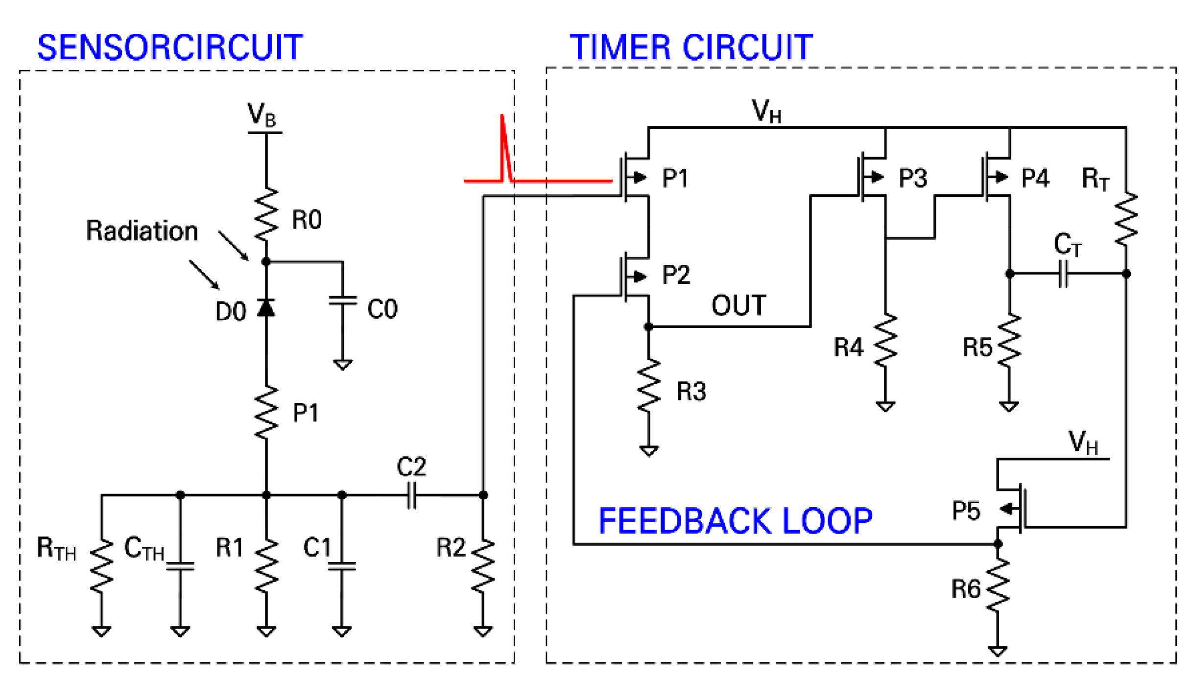
Figure 3 shows a detailed circuit diagram of the proposed detection circuit. The sensor circuit is composed of a PIN diode, resistors, and capacitors. When pulsed radiation is incident on the PIN diode, a photocurrent is generated. After the generated photocurrent is converted to a voltage through the resistors, signals are transmitted to the timer circuit through a differential circuit composed of capacitors and resistors. The detectable voltage level can be adjusted using the RTH and CTH values. The timer circuit is composed of a NOR gate and an inverter of the feedback loop, and is connected to CT and RT, which controls the detection time. It is operated by receiving an input from the sensor circuit, and the output of the sensor circuit is connected to the input of the n-MOSFET (N1) and p-MOSFET (P1) of the NOR gate. In the initial state, the NMOS connected to the ground is off, and the PMOS connected to VH is on; thus, the OUT is kept high. When pulsed radiation is applied and the output of the sensor circuit exceeds the threshold voltage of the input N1 of NOR, N1 is turned on and P1 is turned off.
As a result, the output of NOR, which was kept high, operates at a high speed, and falls to a low level. At this point, the current flows from VH to CT and CT is charged. Even if the output of the sensor circuit falls to a low level after the nuclear pulsed radiation has terminated, the OUT signal is kept low by the timer feedback; thus, CT maintains its charged condition. When charging is completed depending on the capacity of CT, the OUT signal is returned to high. Thus, it was designed for stable and high-speed operation in spite of the simple structure compared with the existing detection circuits.
The functional verification simulation of the proposed circuit designed using the 0.18 um CMOS process device was performed. At the power supply voltage of 3.3 V(VH), the input signal (IN) was applied by modeling a photocurrent that is generated when the sensor detects pulsed radiation. To simulate the input signal photocurrent, first, based on the Fat Man data of Ref. [18], iteratively calculated at 200 m intervals from just below the nuclear explosion (ground range = 0) to 2 km, and the accumulated energy of the sensor (Si, 0.4 mm3) according to the distance (MeV/kt) was obtained. At this time, the position of the sensor was 1 m above the ground. The total amount of energy (MeV/sec/kt) during the time when prompt gamma rays are generated (10 ns–1 us) was calculated based on the time-dependent energy spectrum data of Ref. [19], and the two results calculated in this way re-normalized the gamma-ray energy rate according to time was performed to equal.
Figure 4 shows the result of converting the unit of energy rate to re-normalized prompt gamma rays from MeV/sec/kt to rad/sec/kt. At this time, the unit conversion factor was 1 MeV = 1.71981 × 10⁻⁵ rad, and the detection range was set to 2 × 10⁵–2 × 10⁷ rad/sec considering the distance from the blast core. As shown in Figure 5, the linear increase characteristics of the photocurrent according to the dose rate of the silicon PIN diode sensor to be fabricated were confirmed. Accordingly, the input photocurrent used for the simulation was 2 mA with a pulse width of 1 us corresponding to the minimum detection range.
As shown in the simulation result in Figure 6, the signal of the pulsed radiation converted from photocurrent to voltage is applied to the input of the NOR gate and the detecting signal is outputted at a high speed. A feedback loop is then formed by the CT of the timer circuit, and the signal is reset after a certain period of time, depending on the capacity of CT, and returns to a high state. It is also possible to change the pulse width of the detected signal linearly by fixing the capacitor value of the CT and fine-tuning the variable resistor RT.

2.3. Proposed Pulsed-Radiation Detection Circuit Layout and Simulation

The conventional detection circuit, timer bypass detection circuit, and fast-switching CMOS-logic detection circuit were designed using the same 0.18 um CMOS process conditions, and the response delay time simulation was performed. Figure 7 shows the response time simulation result of each circuit. The reference of the low level of the detected signal used for comparison of the response delay time of each circuit was 0.4 V. A response delay time of 21.4 ns was required to change the output to a low level in the case of the conventional circuit, and 17.6 ns for the timer bypass circuit. In contrast, the response delay time of the fast-switching CMOS-logic pulse-signal detector was 15.8 ns; this is equivalent to an approximate 26% improvement compared with that of the conventional circuit. The fast-switching CMOS-logic detection circuit shortened the delay time owing to its resistance. Because there was no current limit according to resistance, it has the advantage in that it can be designed in practice to achieve a higher speed than the simulation result by adjusting the W/L ratio of the MOSFET. Moreover, compared with the conventional circuit, the stable output can be observed without offset in the high/low state of the detected signal. As shown in Figure 8, when the conventional, timer bypass, proposed, and p-MOSFET-based proposed circuits operate under the same conditions, the average current consumptions are 11 mA, 7.8 mA, and 0.87 mA, respectively. Thus, the proposed circuit can reduce the average current consumption by approximately 92% or more compared with the conventional circuit. Additionally, although the average operating current of the proposed circuit based on p-MOSFET, which will be mentioned later, increases to about 9.5 mA, it has high tolerance to accumulated radiation. Therefore, there is a negative relationship between the radiation tolerance and the current consumption.
When the pulsed-radiation detection circuit is designed using the CMOS bulk process, the TID effects of the n-MOSFET, which is vulnerable in a cumulative radiation environment, should be considered as shown in Figure 9. The n-MOSFET subjected to 1 Mrad of a cumulative dose experienced performance degradation of the device by forming an abnormal leakage current path owing to hole trapping by radiation accumulated at the interface between the insulating oxide and silicon. However, damage by cumulative radiation rarely occurs in the p-MOSFET, unless it is a narrow type, because the carriers forming the default channel consist of holes (among others) [20].
The use of the design of the CMOS logic-based detection circuit proposed in this study as a detection circuit that is resistant to TID effects, consisting of p-MOSFET and passive elements, can be achieved by replacing the n-MOSFETs with resistors. Figure 10 shows the replaced circuit diagram, and the entire circuit can be controlled only by the switching operation of the p-MOSFET. The radiation-tolerant pulsed-radiation detection circuit maintains the advantages of the conventional CMOS logic-detection circuit, such as the fine adjustment of the detected signal pulse width, stable output, and low-power consumption. However, it has a disadvantage in that the output speed of the detection signal is somewhat low owing to the current limit of the resistor that was used instead of the n-MOSFET.
The response time simulation was performed when the design of the fast-switching CMOS logic-based detection circuit was modified to use only p-MOSFETs to block the TID effects. As a result, the response delay time of 15.8 ns was generated when the output of the proposed CMOS logic-based circuit was changed to low, but the response time of the p-MOSFET logic-based circuit increased to 28.2 ns. However, when considering the rise time of initial nuclear pulsed radiation, it takes more than 100ns to reach the latch-up of the CMOS device, so there is no effect on electronic devices within the detection time of 50 ns [16]. Hence, it has the advantage of radiation hardening for TID effects by applying the high-speed CMOS logic-based detection circuit. The specifications of each circuit, including the proposed detection circuit, are summarized in Table 1.

2.4. Implementation of Detection Circuit Chip

The switching CMOS logic-based pulsed-radiation detection circuit proposed in this study was designed based on the SKhynix/Magnachip 0.18 um CMOS bulk process. The circuit was configured using 3.3 V MOSFETs. Finally, a radiation-hardened detection circuit based on p-MOSFET switching that is tolerant to the TID effect was fabricated. Figure 11a shows the layout drawing of the proposed circuit, and Figure 11b shows the photograph of the proposed pulsed-radiation detector package chip that contains a PIN diode and a test light-emitting diode (LED).
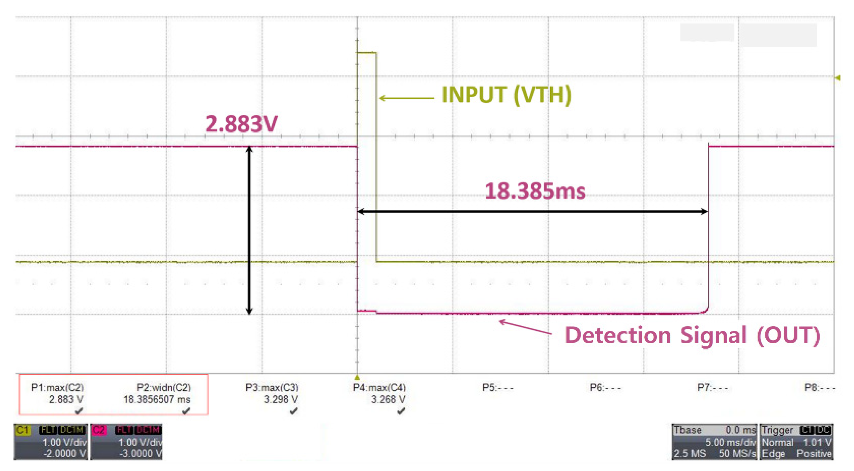
Figure 12 shows the measurement results of the proposed switching detection circuit. The pulsed radiation was simulated by the LED and the photodiode was activated by the LED with a bias voltage applied. The detection circuit was activated when a pulse signal with a voltage above a certain value according to the value of RTH for which the detection level was designed to be adjustable. Furthermore, detection signals with specific widths (18.4 ms) are outputted according to the value of CT, which is designed to enable adjustment of the pulse width of the detection signal. The normal operation of the detection signal was confirmed because it was outputted by the input pulse signal and returned after it was maintained for a certain period of time.
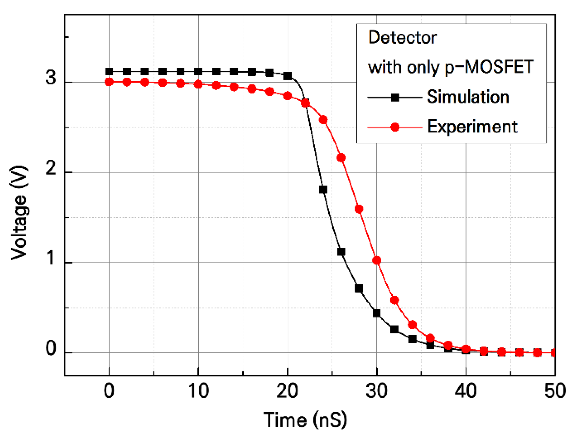
Figure 13 shows the response time measurement result of the proposed p-MOSFET-based detection circuit that is resistant to TID effects. Although a delay of approximately 5 ns occurred compared with the simulation result, it operated at 33 ns. Thus, the detection signal can perform the pulsed radiation detection and protection functions normally. Therefore, the proposed CMOS logic-based detection circuit has the advantage of being applied in various ways according to the radiation environment, because the modified design is still possible using only p-MOSFETs.

3. Radiation-Hardened Detection Circuit Radiation Test Evaluation

3.1. Test Evaluation of Pulsed-Radiation Transient Effects

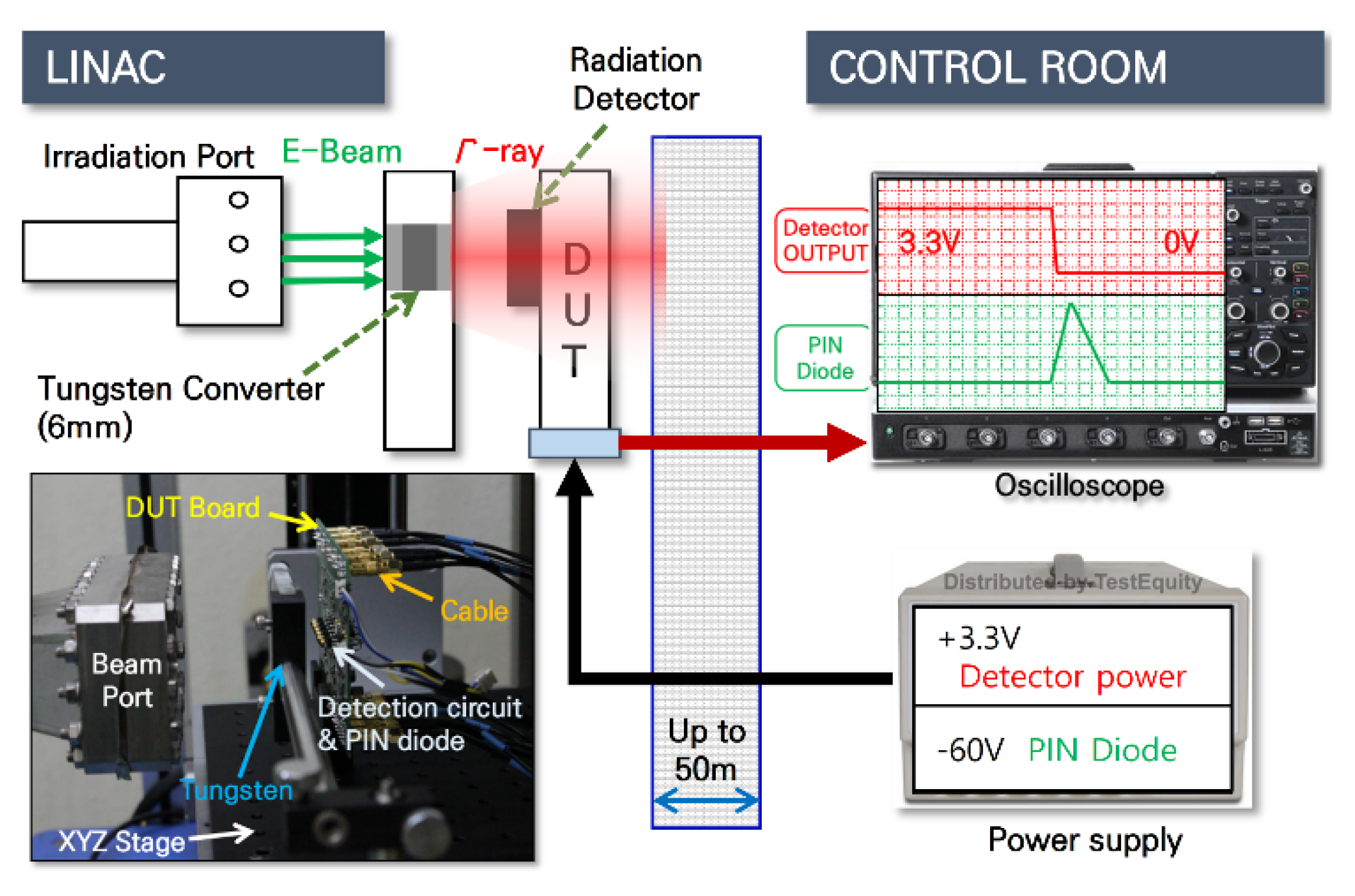
The evaluation test of the pulsed-radiation detection circuit was performed using the LINAC at the PAL. Figure 14 shows the test setup. The electron beam (60 MeV, 180 mA) outputted from the electron beam accelerator was converted to a pulse gamma ray using the tungsten transducer, and was then radiated to the detector. The measurement evaluation procedure used to verify the latch-up and disturbance thresholds of the semiconductor components caused by the pulsed radiation (responsible for the transient effect) was applied. As shown in Figure 14, the DUT board of the sample was installed in the irradiation room, and the process of checking whether the test sample operates normally or not was performed before irradiation. Whether the beam output intensity is adjusted according to the test requirements was assessed by adjusting the beam spot of the electron beam output. Subsequently, the properties of the radiation sensor (PIN diode) and detection circuit were evaluated by measuring the transient response characteristics of the devices according to the transient radiation pulse under the irradiation conditions. Through this process, the threshold resistance value of the required radiation detection range was obtained, and the normal pulse radiation detection function could thus be verified in the set detection range. This test procedure was established based on the procedure specified in MIL-STD-883H 1020.1, which is an electronic component test procedure of the U.S. Department of Defense [21].
The pulsed gamma rays were normalized using the second dosimeter (Thermoluminescence Dosimeter, TLD) while repeated beam irradiation was performed several tens of times while they were inputted to the custom-made PIN diode through the tungsten transducer. The pulsed radiation detection range was found to generate an output in the range of 0.7–22 V in a state at which a 60 V reverse bias was applied with a dose in the range of 1.7 × 10⁵–1.3 × 10⁸ rad(Si)/s. Figure 15 shows the output voltage of the PIN diode according to the dose range.
In this study, a pulsed radiation experiment was conducted to find the value of resistance Rth which corresponded to the detection range of 2.0 × 10⁵–2.0 × 10⁷ rad(si)/s for the switching detection circuit based on the p-MOSFET proposed in this study. Whether the p-MOSFET detection circuit operated according to the radiation dose was evaluated while Rth was changed, and the PIN diode output voltage was measured accordingly. By measuring the dose and threshold voltage at which the detection circuit operated for each resistance Rth, the resistance values were found to lie in the range of 86 Ω–7 kΩ in correspondence to a detection range of 2.0 × 10⁵–2.0 × 10⁷ rad(si)/s, as shown in Figure 16.
The resistance (Rth) was set to 7 kΩ, which corresponds to the detection range 2.0 × 10⁷ rad(si)/s (error rate 10%) of the proposed detection circuit, and the beam was then radiated. The electron beam was repeatedly radiated because it was not uniform. The detected dose was verified by the output voltage of the PIN diode. As a result of the verification of the operation of the detection circuit according to the radiation dose, as shown in Figure 17, it did not operate at a dose (8.99 V) below the detection range, but the detection circuit operated in the detection range (9.06 V).
At this time, about 300 ns time passed until the beam pulse was applied to the sensor and the detection signal was output. This is due to the delay time of the 50 m cable and signal output equipment checking the output from the irradiation room to the control room. The 50 m cable (RG-174/U) used in the test has a signal delay of about 250 ns [22]. Therefore, the operating speed of 50 ns or less of the proposed detection circuit was confirmed.

3.2. Test Evaluation of the TID Effects

In this study, the TID damage evaluation test for the improved p-MOSFET-based detection circuit was conducted to secure tolerance to cumulative radiation of the CMOS logic-based switching pulsed-radiation detection circuit proposed in this study. The test was conducted in the high-level gamma ray irradiation facility at the Advanced Radiation Technology Institute (ARTI) in Jeongeup, Korea. A total cumulative radiation of 2 Mrad was radiated at a dose of 1 Mrad/h using a Cobalt-60 gamma-ray source. The test procedure followed the TID test procedure and evaluation method for electronic components of the MIL-STD-883H 1019.8 and ESA/SCC Basic Specification No.22900 [23,24]. Changes in electrical characteristics according to the cumulative dose for each step were measured by measuring the pulse width and peak voltage of the detected signal when the input pulse was applied to the p-MOSFET detection circuit prototype. At this time, the input pulse was applied by modeling the case wherein the detection circuit was exposed to pulsed radiation because the input pulse was directly applied to the circuit.
Regarding the TID measurement test setup shown in Figure 18, it was divided into a control room for applying and measuring signals and an irradiation room. A 25 m data cable was used to connect the control room to the DUT installed inside the irradiation room. The device used for the application of a bias to the test sample and the measurement system used to monitor the changes in the electrical parameters of the test samples according to the cumulative dose were installed in the control room and were configured to allow remote measurement. The experimental conditions and methods are summarized in the Table 2.
The TID measurement test result of the proposed detection circuit is shown in Figure 19. An observation of the changes in the output according to the rising cumulative dose confirmed that the peak voltage was not changed. The pulse width of the output signal decreased by approximately 3.4 ms from 18.4 ms before irradiation to 15 ms after irradiation.
However, this pulse width change does not cause any problem in executing the detection function. Therefore, the normal operation of the detection circuit within the cumulative dose of 2 Mrad was confirmed by the irradiation experiment. The 1 Mrad data were considered to be data whose characteristics were restored by an annealing time of ~5 min. Therefore, the proposed CMOS logic-based switching detection circuit could execute normal pulsed-radiation detection operations and protection missions in the cumulative radiation environment and based on applications which use only the p-MOSFETs.

4. Conclusions

The proposed CMOS or p-MOSFET switching-based detection circuits proposed in this study detected pulsed radiation at high speed and transmitted detected signals to the circumvention circuit. Compared with the conventional detection circuit, the proposed detection circuit has the advantages of higher response speed (~10% improvement), low-power consumption (92% improvement), and resistance to TID effects. These advantages were verified through simulation and radiation tests. The proposed detection circuit based on p-MOSFET switching was finally fabricated as a packaged chip, including an integrated circuit chip of the 0.18 um CMOS process, radiation sensors, and test LEDs. Its detection function was verified at the predefined pulsed-radiation detection range of 2.0 × 10⁷ rad(si)/s (error rate 10%) through an electron beam accelerator of the test LINAC at the PAL. Its tolerance to TID effects was verified up to 2 Mrad in a high-level gamma ray irradiation facility at the ARTI.
The proposed switching-based detection circuit was flexibly applicable to electronic systems in various fields because it is integration-ready, high speed, and radiation resistant, and prevents disturbance holes and latch-up phenomena by controlling the power source of major electronic systems. Therefore, it is expected that major electronic devices could operate safely even in emergencies in which they are exposed to pulsed radiation.

Author Contributions

Conceptualization, M.L. and N.L.; methodology, M.L. and S.C.; software, M.L. and Y.H.; validation, S.C., M.L. and N.L.; investigation, H.G. and J.K.; data curation, H.G. and J.K.; writing—original draft preparation, M.L. and N.L.; writing—review and editing, S.C. and M.L.; visualization, Y.H.; supervision, S.C.; project administration, N.L. All authors have read and agreed to the published version of the manuscript.

Funding

This work was supported by the KAERI institutional R&D program (Project No. 523420-22), and this research was supported by the National Research Foundation of Korea (NRF) funded by the Korea government (MSIT: Ministry of Science and ICT) (No. RS-2022-00144110). This work was supported by the IDEC.

Data Availability Statement

Not applicable.

Conflicts of Interest

The authors declare no conflict of interest.

References

  1. Edward, C.E. Radiation effects research in the 60’s. IEEE Trans. Nucl. Sci. 1994, 41, 2648–2659. [Google Scholar]
  2. Stassinopoulos, E.; Raymond, J.P. The space radiation environment for electronics. Proc. IEEE 1988, 76, 1423–1442. [Google Scholar] [CrossRef]
  3. Srour, J.R.; McGarrity, J.M. Radiation Effects on Microelctronics in Space. Proc. IEEE 1988, 76, 1443–1469. [Google Scholar] [CrossRef]
  4. Messenger, G.C.; Ash, M.S. The Effects of Radiation on Electronic Systems; Springer Press: Van Nostrand Reinhold, NY, USA, 1992. [Google Scholar]
  5. Alexander, D.R. Transient Ionizing Radiation Effects in Devices and Circuit. IEEE Trans. Nucl. Sci. 2003, 50, 565–582. [Google Scholar] [CrossRef]
  6. Holmes-Siedle, A.; Adams, L. Handbook of Radiation Effects, 2nd ed.; Oxford University Press: Oxford, UK, 2002. [Google Scholar]
  7. Gregory, B.L.; Shafer, B.D. Latch-Up in CMOS Integrated Circuits. IEEE Trans. Nucl. Sci. 1973, 20, 293–299. [Google Scholar] [CrossRef]
  8. Cohn, L.; Espig, M.; Wolicki, A.; Simons, M.; Rogers, C. Transient Radiation Effects on Electronics(TREE) Handbook; Defense Nuclear Agency: Alexandria, VA, USA, 1996. [Google Scholar]
  9. Larry, L. 18 August 1987. Nuclear Event Detector. Available online: http://www.freepatentsonline.com/4687622.pdf (accessed on 10 August 2022).
  10. Douglas, G.C. 9 March 1971. Solid State Crowbar Circuit. Available online: http://www.freepatentsonline.com/3569784.pdf (accessed on 10 August 2022).
  11. Barnaby, H.J. Total-Ionizing-Dose Effects in Modern CMOS Technologies. IEEE Trans. Nucl. Sci. 2006, 53, 3103–3120. [Google Scholar] [CrossRef]
  12. Oldham, T.R.; Mclean, F.B. Total Ionizing Dose Effects in MOS Oxides and Devices. IEEE Trans. Nucl. Sci. 2003, 50, 483–496. [Google Scholar] [CrossRef]
  13. Fleetwood, D.M.; Winokur, P.S.; Reber, R.A.; Meisenheimer, T.L.; Schwank, J.R.; Shaneyfelt, M.R.; Riewe, L.C. Effects of oxide traps, interface traps, and ‘border traps’ on metal-oxide-semiconductor devices. J. Appl. Phys. 1993, 73, 5058–5074. [Google Scholar] [CrossRef]
  14. Karna, S.P.; Pineda, A.C.; Pugh, R.D.; Shedd, W.M.; Oldham, T.R. Electronic structure theory and mechanisms of the oxide trapped hole annealing process. IEEE Trans. Nucl. Sci. 2000, 47, 2316–2321. [Google Scholar] [CrossRef]
  15. Oldham, T.R.; Lelis, A.J. Post-Irradiation Effects in Field-Oxide Isolation structures. IEEE Trans. Nucl. Sci. 1987, 34, 1184. [Google Scholar] [CrossRef]
  16. Ker, M.D.; Hsu, S.F. Transient-Induced Latchup in CMOS Integrated Circuits; John Wiley & Sons Ltd.: Hoboken, NJ, USA, 2009; pp. 33–37. [Google Scholar]
  17. Maxwell Technologies Inc. HSN-1000 Nuclear Event Detector. Available online: https://pdf1.alldatasheet.com/datasheet-pdf/view/124266/MAXWELL/HSN-1000.html (accessed on 14 September 2022).
  18. Reassessment of the Atomic Bomb Radiation Dosimetry for Hiroshima and Nagasaki—Dosimetry System 2002(DS02); Radiation Effects Research Foundation: Hiroshima, Japan, 2005.
  19. Samuel, G.; Philip, J.D. The Effects of Nuclear Weapons, 3rd ed.; U.S. Department of Defense: Washington, DC, USA, 1979; 328p.
  20. Gillardin, M.; Goiffon, V.; Girard, S.; Martinez, M.; Magnan, P.; Paillet, P. Enhanced Radiation-Induced Narrow Channel Effects in Commercial 0.18 um Bulk Technology. IEEE Trans. Nucl. Sci. 2011, 58, 2807–2815. [Google Scholar] [CrossRef]
  21. MIL-STD-883H 1020.1; Dose Rate Induced Latchup Test Procedure; U.S. Department of Defense: Washington, DC, USA, 2010.
  22. GPS Source Inc. CALCULATING the Propagation Delay of Coaxial Cable. Available online: https://studylib.net/doc/18203254/calculating-the-propagation-delay-of-coaxial-cable (accessed on 14 September 2022).
  23. MIL-STD-883H 1019.8; Ionizing Radiation (Total Dose) Test Procedure; U.S. Department of Defense: Washington, DC, USA, 2010.
  24. Total Dose Steady-State Irradiation Test Method; ESA/SCC Basic specification No. 22900 Issue 4; European Space Agency: Paris, France, 2010.
Figure 1. Block diagram of conventional pulsed radiation detection circuits: (a) Maxwell’s nuclear event detector and (b) timer bypass detection circuit.
Electronics 11 02970 g001
Figure 2. Block diagram of the proposed complementary metal-oxide semiconductor (CMOS) logic fast-switching pulsed-radiation detection circuit.
Electronics 11 02970 g002
Figure 3. Detailed view of the proposed detection circuit.
Electronics 11 02970 g003
Figure 4. Simulation result of energy rate (rad/sec/kt) accumulated in Si sensor according to distance and time by prompt gamma rays (HOB is 503 m [18] and the sensor is located 1 m above the ground).
Electronics 11 02970 g004
Figure 5. PIN diode photocurrent characteristic simulation result according to the calculated radiation dose.
Electronics 11 02970 g005
Figure 6. Functional verification simulation of the proposed pulsed radiation detection circuit.
Electronics 11 02970 g006
Figure 7. Response time simulation result of the pulsed-radiation detection circuit.
Electronics 11 02970 g007
Figure 8. Operating current simulation result of the pulsed-radiation detection circuit (at pulse width, 2.3 ms).
Electronics 11 02970 g008
Figure 9. Leakage current measurement result according to the cumulative radiation of n-MOSFET and p-MOSFET (at 1 Mrad).
Electronics 11 02970 g009
Figure 10. Switching-based pulsed-radiation detection circuit that only contains p-MOSFETs.
Electronics 11 02970 g010
Figure 11. Proposed pulsed-radiation detection circuit: (a) 0.18 um CMOS bulk process layout drawing, (b) photograph of the inner part of the package chip that contains the test light-emitting diode and PIN diode.
Electronics 11 02970 g011
Figure 12. Functional verification measurement result of the proposed pulsed-radiation detection circuit.
Electronics 11 02970 g012
Figure 13. Response time measurement result of the proposed pulsed-radiation detection circuit.
Electronics 11 02970 g013
Figure 14. Transient effect test evaluation setup of the pulsed radiation detector.
Electronics 11 02970 g014
Figure 15. Output voltage measurement normalized PIN diode according to radiation dose.
Electronics 11 02970 g015
Figure 16. Dose detection range of proposed radiation detection circuit according to the Rth resistance.
Electronics 11 02970 g016
Figure 17. Detection function measurement outcome according to the dose of the proposed pulsed-radiation detection circuit (@ 2.0 × 10⁷ rad(si)/s).
Electronics 11 02970 g017
Figure 18. TID effect test evaluation setup of the pulsed gamma ray detection circuit.
Electronics 11 02970 g018
Figure 19. TID effect measurement test result of the proposed detection circuit.
Electronics 11 02970 g019
Table 1. Comparison of performances of pulsed-radiation detection circuits based on CMOS.
ParameterConventionalTimer BypassProposed Switching
CMOS LogicOnly p-MOSFET
Response time [ns]21.417.615.828.2
Average operation current * [mA]117.80.879.5
TID toleranceNoNoNoYes
* The pulse width of detection signal is 2.3 ms.
Table 2. TID effect test conditions and test method of pulsed-radiation detection chip.
Irradiation Condition
Total Dose2 Mrad
Dose Rate1 Mrad/h
Radiation SourceCobalt-60
Test FacilityHigh energy γ-ray irradiation facility
Test Method
Sample3 sample
Radiation Step 8 steps (0.25 Mrad/step)
Term of Elec. Param.Output pulse width, Peak voltage
Temperature Condition
IrradiationTA = 25 °C (Room Temperature)
AnnealingTA = 25 °C (Room Temperature)
Publisher’s Note: MDPI stays neutral with regard to jurisdictional claims in published maps and institutional affiliations.