
Power Compression and Phase Analysis of GaN HEMT for Microwave Receiver Protection
by
 ,
,
Wenhan Song
1,2,3, 
Haowen Guo
1,
Yitian Gu
1,2,3,
Junmin Zhou
1,2,3,
Jin Sui
1,2,3,
Baile Chen
1,
Wei Huang
4 and
Xinbo Zou
1,5,* 1
School of Information Science and Technology, ShanghaiTech University, Shanghai 201210, China
2
Shanghai Institute of Microsystem and Information Technology, Chinese Academy of Sciences, Shanghai 200050, China
3
University of Chinese Academy of Sciences, Beijing 100049, China
4
Institute of Microelectronics, Fudan University, Shanghai 200433, China
5
Shanghai Engineering Research Center of Energy Efficient and Custom AI IC, Shanghai 200031, China
*
Author to whom correspondence should be addressed.
Electronics 2022, 11(13), 1958; https://doi.org/10.3390/electronics11131958
Submission received: 25 May 2022
/
Revised: 12 June 2022
/
Accepted: 13 June 2022
/
Published: 22 June 2022
(This article belongs to the Special Issue GaN-Based Power Electronic Devices and Their Applications)
Abstract
:This paper reports a high-performance microwave receiver protector (RP) based on a single gallium nitride (GaN) high electron mobility transistor (HEMT) at an operation frequency of 30 to 3000 MHz. The HEMT-based RP exhibits multi features: high power compression, constant output power, tunable threshold power level, and insensitivity to frequency variation. With a low drain voltage (Vds) of 3 V, constant output power of 9.9 dBm was acquired for input power over its threshold power of 3.2 dBm. Power compression of 13.3 dB was achieved at the input power of Pin = 20 dBm. In addition, adjustable threshold power level Pth could be obtained by merely tuning drain voltage. Transducer gain measurement results were employed to explain the occurrence of output power saturation. Relatively higher Pth was linked to wider gate voltage swing which extended the linear region of the Pout-Pin characteristic. In addition, the GaN HEMT’s power compression capability shows great immunity to frequency variation, which is promising for protecting sensitive receiver components at both low and high frequencies. Finally, the phase shift of the GaN HEMT RP at high input power was measured and analyzed by the nonlinear behaviors of input capacitance Cgs.
1. Introduction
Receiver protectors (RPs) are widely used to provide protection to radio frequency (RF) and microwave receivers and components, such as low noise amplifiers (LNAs) [1,2] and analog-to-digital converters (ADCs) [3,4]. An RP allows input power below a certain value to pass through ideally without loss, and attenuating input signal strength when it exceeds the threshold. A number of device technologies have been developed to achieve RF and microwave RPs, including Schottky barrier diodes (SBDs) [5,6,7], p-i-n diodes [3,8,9], and transistors [10,11,12]. Employing a steep-mesa technology, a gallium nitride (GaN) SBD based RP demonstrated a low on-resistance (RON) and a power compression of 3.3 dB with a corresponding input power of 20 dBm at 2 GHz [7]. A low insertion loss of 0.3 dB has also been reported for a diamond diode based RP at an operation frequency of 1 GHz [9]. However, for a diode-based RP, typically a tradeoff often has to be made between Coff and Ron [7,8,9]. Although diode-based RPs have made steady progress, they still face some important challenges, such as insufficient power compression, inadequacy in tuning their threshold power level (the input power with 1-dB gain compression), and sensitivity to frequency change. Some attempts, including reverse-biased configurations, stacked antiparallel configurations, etc. have been enacted to mitigate the issues [3,13]; however, most of the efforts required complex circuits to work with. Transistors have been regarded as another viable option for RF RPs. The basic principle of transistor-based RPs is to operate the transistors in their saturation region to limit the output power [10,14,15]. Owing to their saturated output power, RPs formed by transistors possess the advantages of constant output power and outstanding power compression capability.
AlGaN/GaN-based high electron mobility transistors (HEMTs) with embedded 2-dimension electron gas (2DEG) have been widely used in power amplifiers (PAs) [16,17], RF switches [18,19] and LNAs with extremely short recovery time [20,21], due to superior properties such as high power density at high frequencies, high breakdown voltages and large carrier density and mobility [22,23,24].
In this paper, we demonstrated a microwave RP based on a single GaN HEMT on Silicon carbide (SiC) substrate. The HEMT receiver protector offers a certain gain for the small input signal and attenuates input signal strength beyond the threshold power into a constant output power. The threshold power could be well adjusted by varying the bias. It is also demonstrated that the power reduction capability was hardly sensitive to working frequency. Moreover, the phase shift—a critical issue when an RP was applied in high performance phased-array receiver front end [25]—was investigated and analyzed by the small RF signal measurements. The results paved a solid path for a single GaN HEMT to form an RP with high power compression, threshold power adjustability, and frequency stability.
2. Materials and Methods
The GaN-based HEMT used in this study was grown and fabricated on a SiC substrate as shown in Figure 1a. The epitaxial structure includes an Al0.25Ga0.75N barrier layer, a GaN layer buffer layer, and an AlN nucleation layer. The fabrication process of the HEMT started with mesa isolation, which was completed in Inductive Coupled Plasma Reactive Ion Etching (ICP-RIE) and wet etching in 5% TMMA at 50 °C. Then, the ohmic contact was formed by depositing Ti/Al/Ni/Au (20/150/50/80 nm), followed by annealing at 850 °C for 45 s. Finally, a Ni/Au (50/150 nm) Schottky metal was evaporated as the gate and interconnection. The gate terminal was fabricated into a rectangular shape with its length and width of 1.2 µm and 100 µm, respectively, and the distances between gate to source and to drain were 1.5 μm and 2 μm (Lg = 1.2 μm, Lgs = 1.5 μm, Lgd = 2 μm, Wg = 100 μm).
The setup shown in Figure 1b was used for power compression measurements of the GaN HEMT RP. To investigate the power limiting performance of the GaN HEMT at various frequencies, an on-wafer GaN HEMT measurement was conducted without being constrained by the matching network. The input RF signal which was generated by the signal generator (Rohde & Schwarz SMA100B) was injected into the gate using a bias-tee. The output RF signal was extracted from the drain terminal using a spectrum analyzer. To protect the spectrum analyzer from being overdriven, a 30 dB attenuator was used. Power-dependent measurements at various DC bias voltages and different frequencies were carried out with the aid of a computer based controller. The phase shift derived from the reference value at Pin = −20 dBm was measured by a Vector Network Analyzer (VNA) (Keysight ENA5080A).
3. Results and Discussion
3.1. DC Characteristic
Figure 2a shows the transfer characteristics of the GaN HEMT, with a peak DC transconductance (gm) of 197 mS/mm obtained at Vgs/Vds = −1/3 V. The threshold voltage Vth was determined to be −1.8 V, extracted from the linear extrapolation of the Ids-Vgs curve. Figure 2b depicts the output characteristics of the GaN HEMT, showing saturated drain current density (Idsat) of 667 mA/mm at Vgs = 4 V. The slight drop of the drain current during relatively high drain voltage with Vgs >1 V is due to the self-heating effect (SHE) [26]. Under the field strength of 0.5 MV/cm, the gate leakage current density of this GaN HEMT was measured to be 1.95 × 10⁻³ mA/mm, which is much smaller than the typical gate breakdown standard of 1 mA/mm [27,28], indicating a Vgd breakdown voltage higher than 100 V.
3.2. High Power Compression of the GaN HEMT RP
Figure 3a presents representative output power (Pout) as a function of input power. When the input power was low, the receiver protector offered a fixed gain of 2.9 dB. The results show that Pout increased linearly as injected power was enhanced from −20 dBm to 3.2 dBm, with a fixed gain of 2.9 dB rather than insertion loss typically observed in a diode-based RP. With an input power of 3.2 dBm, a gain reduction of 1 dB was observed. When the input power was further enhanced, the output power began to saturate and was clamped at 9.9 dBm as shown in Figure 3a. The input power level could only reach 21 dBm due to the short length of the Lgd (2 microns), and it could be further improved by some advanced processing technologies, such as a metal-insulator-semiconductor (MIS) HEMT with a gate dielectric [29] or structures with surface passivation [30].
In the shaded area of Figure 3b, the power compression as a function of input power could be well fitted by a linear relationship with a slope of 1 dB per 1dB, which indicated a constant output power. The improvement of the power compression of this GaN HEMT RP was at the expense of DC power consumption.
The GaN HEMT RP in this work presented a better power limiting capability than diode-based RPs reported in the literature [7,31,32]. As shown in Figure 3c, when the injection power was 17 dB higher than individual threshold power levels, the GaN HEMT RP had 2~4 dB more power compression than those diode-base RPs. It was attributed to the saturated output power of the GaN HEMT, while the diode-based RP cannot sufficiently attenuate the input power due to its non-zero on-resistance (Ron) at high input power [33]. Moreover, there was a tradeoff between high power compression and circuit complexity for a diode based RP [34]. The high power compression, as shown in Figure 3b, was challenging to realize for a single-stage diode based RP [3,33]. Therefore, increasing the number of stages was often used to achieve a constant output power at a large input signal, which would increase the size and complexity of the diode based RP circuit. Whereas, for the GaN HEMT-based RP, the circuit complexity only came from the bias circuit.
3.3. Tunable Threshold of the GaN HEMT RP
Figure 4a shows the relationship between the output power and the input power of the GaN HEMT RP at Vgs = −1 V (working frequency of 3 GHz), with three different drain voltages (3/5/10 V). When the Pin was below 3.5 dBm, uniform output power Pout was acquired for all the bias conditions. However, when the Pin was beyond 7 dBm, apparent divergence was spotted as Vds increased from 3 V to 5 V and 10 V. In addition to enhanced output power with increasing Vds, the threshold power level Pth was also enhanced. Threshold power levels Pth of 3.97/6.97/7.97 dBm were extracted from Vds = 3/5/10 V, respectively, indicating that a higher drain bias may extend the linear region of an RP and postpone the occurrence of power saturation.
To investigate the dependence of the threshold power level Pth on the drain voltage Vds, the transducer gain, which was measured at a low input power of −20 dBm, was utilized. Figure 4b depicts transducer gain as a function of Vgs at the frequency of 3 GHz. The gate voltage swing (GVS) [35] for a 9 dB transducer gain drop was determined to be 2.9 V, 4.4 V, and 5.2 V, for Vds = 3/5/10 V, respectively.
A relative wider GVS means the transistor could keep the transducer gain high for an ample range of input power, as the input power was applied at the gate-source terminals. Thus, with a wide GVS, the transistor could allow a broad range of input power through without causing output power to be compressed, as shown in an extended linear region of the Pout-Pin graph [Figure 4a]. As a result, a larger threshold power level Pth could be obtained by merely increasing drain-source bias, and Pth can be easily electronically-tuned by Vds, which contributes to the application of the HEMT based RP in a dynamic environment and the precise protection of sensitive devices [13,36]. It should also be noted that reducing the Lg of a GaN HEMT would enhance the non-uniformity of gm, which could enable the lowering of Pth to protect more power-sensitive devices [37,38]. However, for a p-i-n diode RP, the threshold power level was typically governed by the thickness of the i-layer, and can hardly be adjusted once the device was manufactured [39].
3.4. Frequency Independent HEMT RP
Figure 5a reports the input and output power characteristics of the GaN HEMT based RP at various working frequencies. The measured data show that at a given Vds, the GaN HEMT based RP exhibited typically the same power compression capability and threshold power level over a wide frequency range from 30 MHz to 3 GHz. For example, at a Vds of 3 V, the maximum output power and Pth were extracted to be 9.86 0.3 dBm and 2.81 0.4 dBm, respectively, showing little divergence among various operation frequencies from 30 MHz to 3 GHz. Whereas, Pth of a p-i-n based RP dropped rapidly as shifting to low operation frequencies due to the transit time of carriers across the i-region is shorter than the signal period time at a low frequency, e.g., Pth was reduced from 20 dBm at 3 GHz to 9 dBm at 30 MHz for a silicon p-i-n diode [31].
Unlike p-i-n based RPs, this GaN HEMT based RP can maintain a good frequency response within its cut-off frequency (ft) of 11.28 GHz. The frequency-insensitive property could be attributed to the uniform transducer gain of the device over a wide operation frequency, as shown in Figure 5b, which shows the transducer gain as a function of frequency for this GaN HEMT. In the range of 30–3000 MHz, an almost steady transducer gain was obtained for either a small RF signal (Pin = −20 dBm) or relatively large RF power (Pin = 5 dBm). As a result, almost identical output power could be expected in the linear region and saturation region of the device. Therefore, constant output power could be achieved at both small and large input power, resulting in a good broadband property without matching circuits. It should be noted that adding a matching network in a real application will not affect the characteristics of the GaN HEMT RP, such as high power compression and tunable threshold power.
The frequency response of this HEMT RP is related to the current cut-off frequency (ft) and maximum oscillation frequency (fmax). It is noted that the device used in this study featured a gate length of 1.2 μm and held an ft of 11.28 GHz and an fmax of 22.35 GHz, respectively. It is expected that the frequency steadiness property could be extended to an even higher frequency on shrinking the gate length dimension [40,41,42]. Based on its frequency-insensitive property, GaN HEMT could be used to protect sensitive components such as mixers in transmitters over a large frequency range. In addition, it paved a path to improving the frequency response without using multiple devices or auxiliary circuits [3].
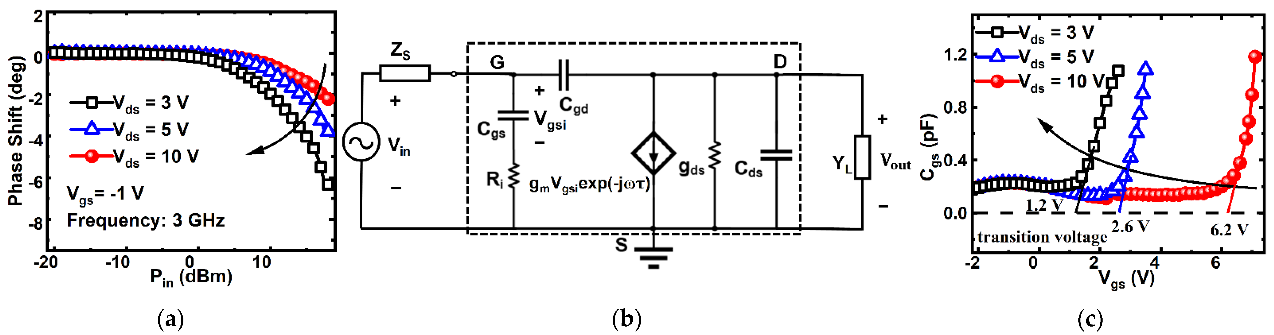
3.5. Phase Shift Analysis of the HEMT RP
Figure 6a illustrates the phase shift of GaN HEMT based RP with different Vds. The output phase was typically unchanged when the device was fed with a small input power lower than 0 dBm. However, as Pin increased, the phase dropped dramatically. Phase shift over 1 degree occurred at the Pin of 6.2/10.7/12.7 dBm for Vds = 3/5/10 V respectively.
A small RF signal equivalent circuit model of this GaN HEMT is shown in Figure 6b [43,44]. This model consisted of an input resistance (Ri), an input (Cgs), output (Cds) and feedback (Cgd) capacitors, and a voltage controlled current source (gm·Vgsiexp(-jωτ)) where τ was transconductance delay. The RF power source is modeled by a voltage source and an internal impedance Zs = Rs. The output load is modeled by an admittance YL = GL.
The feedback capacitor Cgd could be ignored due to the fact that it had small value. Therefore, the phase of output voltage could be computed as Equation (1):
Since Cds (at fF level) is much smaller than the input capacitor Cgs, the phase of output voltage could be further simplified as Equation (2):
Thus, the phase of output voltage could be regarded to be merely determined by the Cgs. Cgs could be extracted by the small RF signal equivalent circuit model shown in the dashed box in Figure 6b [44].
Figure 6c shows Cgs as a function of Vgs. For a given Vds, Cgs was unchanged around Vgs = −1 V, which corresponds to a relatively low input power. However, on increasing the input power, which could be interpreted as increasing the Vgs, a dramatically enhanced Cgs was observed. The increase of Cgs would cause a decrease in the phase of output voltage according to Equation (2), resulting in a significant drop in the phase shift at large inputs as shown in Figure 6a.
When Vds was increased from 3 V to 5 V and 10 V, the corresponding transition voltages extracted from the linear extrapolation of Cgs-Vgs curve were also increased from 1.2 V to 2.6 V and 6.2 V, respectively. The lower transition voltage at a relatively smaller drain voltage leads to the early onset of Cgs increasing, which causes the early significant output phase drop at a relatively small Vds when a large power is injected into the gate of the device.
4. Conclusions
High performance microwave RP based on a single GaN HEMT is demonstrated, with features of high power compression, tunable threshold power level, and a frequency-insensitive property. Although additional power was dissipated, constant output power was achieved at large input power owing to the saturated output power of the HEMT RP, indicating a competitive advantage over diode-based RPs. In addition, adjustable Pth was presented and Pth could be easily tuned by adjusting drain voltage. The tunable Pth was well modeled and explained by transducer gain measurement results. The higher Pth was attributed to the wider gate voltage swing, which extended the linear region of the Pout-Pin characteristics. Both Pth and the power compressions are frequency-independent, indicating a good broadband property without matching circuits, which means the GaN HEMT RP could be used to protect ADCs and sensitive receiver components at both low and high frequencies. The phase shift of the GaN HEMT at high input power was measured and analyzed. The occurrence of the phase shift was mainly caused by the nonlinearity of the input capacitor Cgs at a large signal input. It was found that a higher drain voltage would hinder the onset of the phase shift and reduce the extent of the phase shift.
Author Contributions
Conceptualization, W.S., H.G. and X.Z.; methodology, W.S. and H.G.; software, W.S., H.G. and J.Z.; validation, W.S. and J.Z.; formal analysis, W.S. and H.G.; investigation, W.S. and H.G.; resources, W.H. and Y.G.; data curation, W.S.; writing—original draft preparation, W.S. and H.G.; writing—review and editing, J.S. and B.C.; supervision, X.Z.; funding acquisition, X.Z. All authors have read and agreed to the published version of the manuscript.
Funding
This research was funded by ShanghaiTech University Startup Fund 2017F0203-000-14, the National Natural Science Foundation of China (Grant No. 52131303), Natural Science Foundation of Shanghai (Grant No. 22ZR1442300), and in part by CAS Strategic Science and Technology Program under Grant No. XDA18000000.
Conflicts of Interest
The authors declare no conflict of interest.
References
- Zhang, S.; Liu, L.; Xu, J.; Wang, R.; Zheng, P.; Wang, H.; Li, M.; Kong, X.; Tong, X. Robust GaN-Based LNAs with Active Epitaxial Current Limiters. IEEE Microw. Wirel. Compon. Lett. 2021, 31, 1287–1290. [Google Scholar] [CrossRef]
- Mahmoudidaryan, P.; Medi, A. Codesign of Ka-Band Integrated Limiter and Low Noise Amplifier. IEEE Trans. Microw. Theory Tech. 2016, 64, 2843–2852. [Google Scholar] [CrossRef]
- Deng, S.; Gao, C.; Chen, S.; Sun, J.; Wu, K. Research on Linearity Improvement of Silicon-Based p-i-n Diode Limiters. IEEE Microw. Wirel. Compon. Lett. 2020, 30, 62–65. [Google Scholar] [CrossRef]
- Lim, C.-L. [limiter] Limiters protect ADCs: Without adding harmonics. Microw. RF 2015, 54, 56–60. [Google Scholar]
- Dong, Q.; Ma, X.Y.; Hu, H.Q.; Wang, X.J. 18–40 GHz broadband limiter based on Schottky diode. In Proceedings of the 2015 Asia-Pacific Microwave Conference (APMC), Nanjing, China, 6–9 December 2015; Volume 3, pp. 1–3. [Google Scholar] [CrossRef]
- Fan, G.Q.; Xing, H.Y.; Hu, H.Q. K-Ka band schottky diode limiter. In Proceedings of the 2013 IEEE International Conference on Applied Superconductivity and Electromagnetic Devices, Beijing, China, 25–27 October 2013; pp. 160–162. [Google Scholar] [CrossRef]
- Sun, Y.; Kang, X.; Deng, S.; Zheng, Y.; Wei, K.; Xu, L.; Wu, H.; Liu, X. First Demonstration of L-Band High-Power Limiter with GaN Schottky Barrier Diodes (SBDs) Based on Steep-Mesa Technology. Electronics 2021, 10, 433. [Google Scholar] [CrossRef]
- Wang, Z.; Cao, H.; Zhang, C. Research on the influence of PIN diode on limiter performance in power limiter. In Proceedings of the 2017 7th IEEE International Symposium on Microwave, Antenna, Propagation, and EMC Technologies (MAPE), Xi’an, China, 24–27 October 2017; pp. 220–223. [Google Scholar] [CrossRef]
- Surdi, H.; Ahmad, M.F.; Koeck, F.; Nemanich, R.J.; Goodnick, S.; Thornton, T.J. RF Characterization of Diamond Schottky p-i-n Diodes for Receiver Protector Applications. IEEE Microw. Wirel. Compon. Lett. 2020, 30, 1141–1144. [Google Scholar] [CrossRef]
- Szczepaniak, Z.R.; Arvaniti, A. Analysis of microwave X-band HEMT limiters based on self-limiting effect. In Proceedings of the 12th International Symposium on Electron Devices for Microwave and Optoelectronic Applications, EDMO 2004, Kruger National Park, South Africa, 8–9 November 2004; IEEE: Piscataway, NJ, USA, 2004; pp. 19–22. [Google Scholar]
- Campbell, C.F.; Hitt, J.C.; Wills, K. Wideband GaN FET based limiter MMICs. In Proceedings of the Microwave Integrated Circuits Conference, Amsterdam, The Netherlands, 29–30 October 2012. [Google Scholar]
- Echchakhaoui, K.; Abdelmounim, E.; Bennis, H.; Latrach, M. A Novel Zero Bias Microstrip MESFET Power Limiter. In Proceedings of the ICCWCS 2019: Third International Conference on Computing and Wireless Communication Systems, ICCWCS 2019, Kénitra, Morocco, 24–25 April 2019; European Alliance for Innovation: Ghent, Belgium, 2019; p. 185. [Google Scholar]
- Bera, S.C.; Basak, K.; Jain, V.K.; Singh, R.V.; Garg, V.K. Schottky diode-based microwave limiter with adjustable threshold power level. Microw. Opt. Technol. Lett. 2010, 52, 1671–1673. [Google Scholar] [CrossRef]
- Parra, T.; Gayral, M.; Llopis, O.; Pouysegur, M.; Sautereau, J.; Graffeuil, J. Design of a low phase distortion GaAs FET power limiter. IEEE Trans. Microw. Theory Tech. 1991, 39, 1059–1062. [Google Scholar] [CrossRef]
- Bera, S.C. Microwave Active Devices and Circuits for Communication; Springer: Berlin, Germany, 2019. [Google Scholar]
- Shukla, S.; Kitchen, J. GaN-on-Si switched mode RF power amplifiers for non-constant envelope signals. In Proceedings of the 2017 IEEE Topical Conference on RF/Microwave Power Amplifiers for Radio and Wireless Applications (PAWR), Phoenix, AZ, USA, 15–18 January 2017; pp. 88–91. [Google Scholar] [CrossRef]
- Formicone, G.; Burger, J.; Custer, J.; Keshishian, R.; Veitschegger, W. A study for achieving high power and efficiency based on high bias operation in C- and X-band GaN power amplifiers. In Proceedings of the 2018 IEEE Topical Conference on RF/Microwave Power Amplifiers for Radio and Wireless Applications (PAWR), Anaheim, CA, USA, 14–17 January 2018; pp. 39–42. [Google Scholar] [CrossRef]
- Florian, C.; Gibiino, G.P.; Santarelli, A. Characterization and Modeling of RF GaN Switches Accounting for Trap-Induced Degradation Under Operating Regimes. IEEE Trans. Microw. Theory Tech. 2018, 66, 5491–5500. [Google Scholar] [CrossRef]
- Florian, C.; Gibiino, G.P.; Santarelli, A. Assessment of the Trap-Induced Insertion Loss Degradation of RF GaN Switches Under Operating Regimes. In Proceedings of the 2018 IEEE/MTT-S International Microwave Symposium-IMS, Philadelphia, PA, USA, 10–15 June 2018; pp. 732–735. [Google Scholar] [CrossRef]
- Rudolph, M.; Behtash, R.; Doerner, R.; Hirche, K.; Wurfl, J.; Heinrich, W.; Trankle, G. Analysis of the Survivability of GaN Low-Noise Amplifiers. IEEE Trans. Microw. Theory Tech. 2007, 55, 37–43. [Google Scholar] [CrossRef]
- Rudolph, M.; Dewitz, M.; Liero, A.; Khalil, I.; Chaturvedi, N.; Wipf, C.; Bertenburg, R.M.; Miller, J.; Wurfl, J.; Heinrich, W.; et al. Highly robust X-band LNA with extremely short recovery time. In Proceedings of the 2009 IEEE MTT-S International Microwave Symposium Digest, Boston, MA, USA, 7–12 June 2009; pp. 781–784. [Google Scholar] [CrossRef]
- Kumar, V.; Lu, W.; Schwindt, R.; Kuliev, A.; Simin, G.; Yang, J.; Khan, M.A.; Adesida, I. AlGaN/GaN HEMTs on SiC with fT of over 120 GHz. IEEE Electron Device Lett. 2002, 23, 455–457. [Google Scholar] [CrossRef]
- Jatal, W.; Baumann, U.; Tonisch, K.; Schwierz, F.; Pezoldt, J. High-Frequency Performance of GaN High-Electron Mobility Transistors on 3C-SiC/Si Substrates With Au-Free Ohmic Contacts. IEEE Electron Device Lett. 2015, 36, 123–125. [Google Scholar] [CrossRef]
- Song, W.; Zheng, Z.; Chen, T.; Wei, J.; Yuan, L.; Chen, K.J. RF Linearity Enhancement of GaN-on-Si HEMTs With a Closely Coupled Double-Channel Structure. IEEE Electron Device Lett. 2021, 42, 1116–1119. [Google Scholar] [CrossRef]
- Garg, R.; Natarajan, A.S. A 28-GHz Low-Power Phased-Array Receiver Front-End With 360° RTPS Phase Shift Range. IEEE Trans. Microw. Theory Tech. 2017, 65, 4703–4714. [Google Scholar] [CrossRef]
- Chattopadhyay, M.K.; Tokekar, S. Thermal model for dc characteristics of algan/gan hemts including self-heating effect and non-linear polarization. Microelectron. J. 2008, 39, 1181–1188. [Google Scholar] [CrossRef]
- Yang, L.; Yang, L.-A.; Rong, T.; Li, Y.; Jin, Z.; Hao, Y. Codesign of Ka-Band Integrated GaAs PIN Diodes Limiter and Low Noise Amplifier. IEEE Access 2019, 7, 88275–88281. [Google Scholar] [CrossRef]
- Pantellini, A.; Peroni, M.; Nanni, A.; Bettidi, A. Performance assessment of GaN HEMT technologies for power limiter and switching applications. In Proceedings of the 5th European Microwave Integrated Circuits Conference, Paris, France, 27–28 September 2010; IEEE: Piscataway, NJ, USA, 2010; pp. 45–48. [Google Scholar]
- Tang, Z.; Jiang, Q.; Lu, Y.; Huang, S.; Yang, S.; Tang, X.; Chen, K.J. 600-V Normally Off SiNx/AlGaN/GaN MIS-HEMT With Large Gate Swing and Low Current Collapse. IEEE Electron Device Lett. 2013, 34, 1373–1375. [Google Scholar] [CrossRef]
- Kanamura, M.; Kikkawa, T.; Iwai, T.; Imanishi, K.; Kubo, T.; Joshin, K. An over 100 W n-GaN/n-AlGaN/GaN MIS-HEMT power amplifier for wireless base station applications. In Proceedings of the IEEE InternationalElectron Devices Meeting, Washington, DC, USA, 5 December 2005; pp. 572–575. [Google Scholar] [CrossRef]
- Skyworks, Woburn, MA, and USA. CLA Series: Silicon Limiter Diode Bondable Chips. 2015. Available online: https://www.skyworksinc.com/en/Products/Diodes/CLA4609-000 (accessed on 25 May 2021).
- Seymour, D.J.; Heston, D.D.; Lehmann, R.E.; Zych, D. X-band monolithic GaAs PIN diode variable attenuation limiter. In Proceedings of the IEEE International Digest on Microwave Symposium, Dallas, TX, USA, 8–10 May 1990; IEEE: Piscataway, NJ, USA, 1990; pp. 841–844. [Google Scholar]
- Carroll, J.M. Performance comparison of single and dual stage MMIC limiters. In Proceedings of the 2001 IEEE MTT-S International Microwave Sympsoium Digest (Cat. No.01CH37157), Phoenix, AZ, USA, 20–24 May 2001; Volume 2, pp. 1341–1344. [Google Scholar] [CrossRef]
- Jha, V.; Surdi, H.; Ahmad, M.F.; Koeck, F.; Nemanich, R.J.; Goodnick, S.; Thornton, T.J. Diamond Schottky p-i-n diodes for high power RF receiver protectors. Solid-State Electron. 2021, 186, 108154. [Google Scholar] [CrossRef]
- Gao, T.; Xu, R.; Kong, Y.; Zhou, J.; Kong, C.; Dong, X.; Chen, T. Improved linearity in AlGaN/GaN metal-insulator-semiconductor high electron mobility transistors with nonlinear polarization dielectric. Appl. Phys. Lett. 2015, 106, 243501. [Google Scholar] [CrossRef]
- Naglich, E.J.; Guyette, A.C. Frequency-Selective Limiters Utilizing Contiguous-Channel Double Multiplexer Topology. IEEE Trans. Microw. Theory Tech. 2016, 64, 2871–2882. [Google Scholar] [CrossRef]
- Cui, P.; Lv, Y.; Liu, H.; Cheng, A.; Luan, C.; Zhou, Y.; Lin, Z. Effect of different gate lengths on device linearity in AlGaN/GaN high electron mobility transistors. Phys. E Low-Dimens. Syst. Nanostruct. 2020, 119, 114027. [Google Scholar] [CrossRef]
- Yang, M.; Lv, Y.; Feng, Z.; Lin, W.; Cui, P.; Liu, Y.; Fu, C.; Lin, Z. Study of Gate Width Influence on Extrinsic Transconductance in AlGaN/GaN Heterostructure Field-Effect Transistors With Polarization Coulomb Field Scattering. IEEE Trans. Electron Devices 2016, 63, 3908–3913. [Google Scholar] [CrossRef]
- Kyabaggu, P.B.K.; Haris, N.; Rezazadeh, A.A.; Sinulingga, E.; Alim, M.A.; Zhang, Y. Design and realisation of a pHEMT diode MMIC power limiter using 3D GaAs multilayer CPW technology. In Proceedings of the 2015 European Microwave Conference (EuMC), Paris, France, 7–10 September 2015; pp. 522–525. [Google Scholar] [CrossRef]
- Li, L.; Nomoto, K.; Pan, M.; Li, W.; Hickman, A.; Miller, J.; Lee, K.; Hu, Z.; Bader, S.J.; Lee, S.M.; et al. GaN HEMTs on Si With Regrown Contacts and Cutoff/Maximum Oscillation Frequencies of 250/204 GHz. IEEE Electron Device Lett. 2020, 41, 689–692. [Google Scholar] [CrossRef]
- Zhang, X.W.; Jia, K.J.; Wang, Y.G.; Feng, Z.H.; Zhao, Z.P. AlNGaN HEMT T- gate optimal design. Appl. Mech. Mater. 2013, 347, 1790–1792. [Google Scholar] [CrossRef]
- Chung, J.W.; Hoke, W.E.; Chumbes, E.M.; Palacios, T. AlGaN/GaN HEMT With 300-GHz fmax. IEEE Electron Device Lett. 2010, 31, 195–197. [Google Scholar] [CrossRef]
- Alim, M.A.; Rezazadeh, A.A.; Gaquiere, C. Temperature Effect on DC and Equivalent Circuit Parameters of 0.15-μm Gate Length GaN/SiC HEMT for Microwave Applications. IEEE Trans. Microw. Theory Tech. 2016, 64, 3483–3491. [Google Scholar] [CrossRef]
- Berroth, M.; Bosch, R. Broad-band determination of the FET small-signal equivalent circuit. IEEE Trans. Microw. Theory Tech. 1990, 38, 891–895. [Google Scholar] [CrossRef] [Green Version]
Figure 1.
(a) Micrographs of GaN HEMT grown and fabricated on SiC with GSG test module; (b) the test setup of this HEMT RP experiment diagram.
Figure 1.
(a) Micrographs of GaN HEMT grown and fabricated on SiC with GSG test module; (b) the test setup of this HEMT RP experiment diagram.
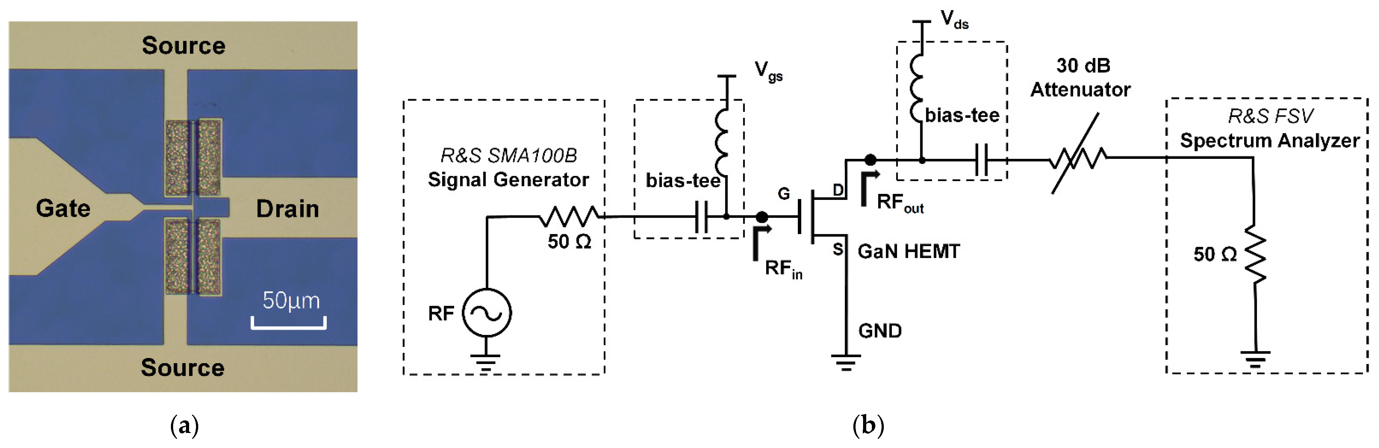
Figure 2.
(a) Transfer characteristics at Vds = 3 V; (b) output characteristics as Vgs increases from −3 V to 4 V with a step of 1 V.
Figure 2.
(a) Transfer characteristics at Vds = 3 V; (b) output characteristics as Vgs increases from −3 V to 4 V with a step of 1 V.
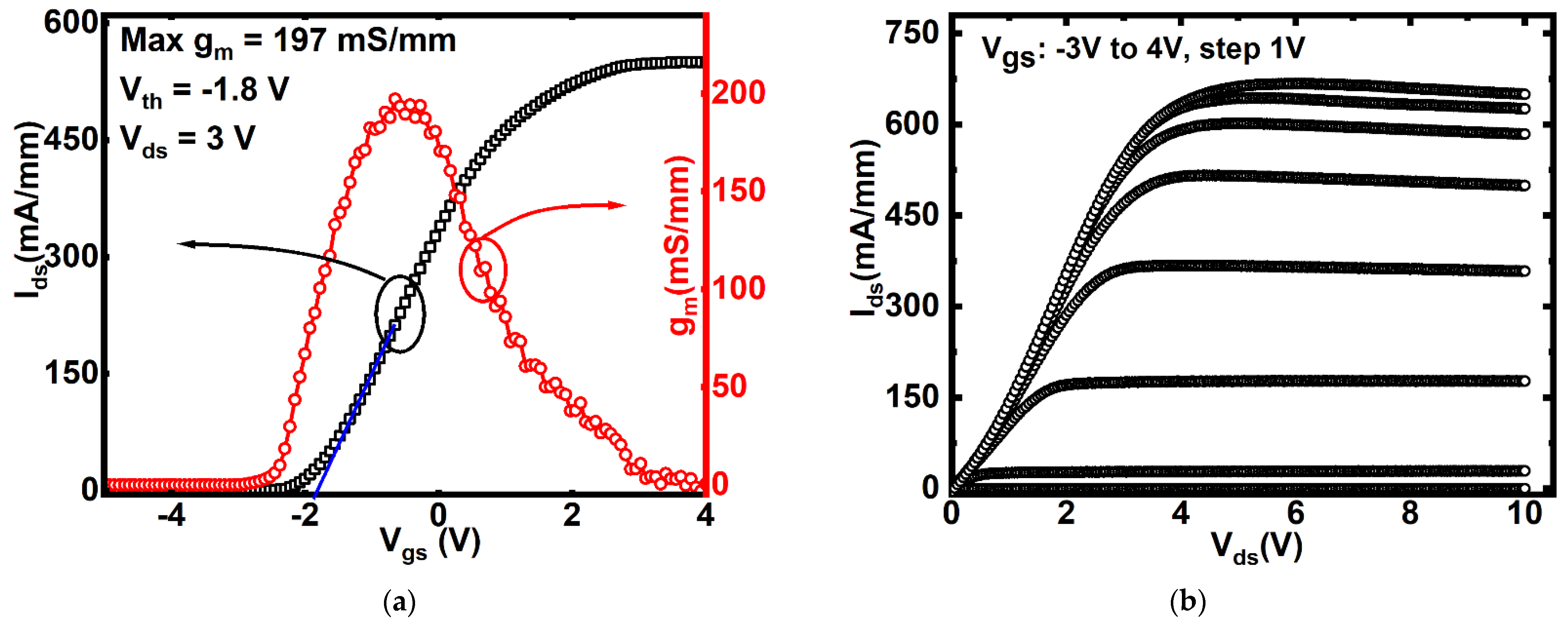
Figure 3.
(a) Output power (Pout) versus input power (Pin) for the single GaN HEMT RP at 3 GHz; (b) power compression as a function of Pin; (c) comparison of the power compression between this single GaN HEMT and diode–based RPs in the literatures.
Figure 3.
(a) Output power (Pout) versus input power (Pin) for the single GaN HEMT RP at 3 GHz; (b) power compression as a function of Pin; (c) comparison of the power compression between this single GaN HEMT and diode–based RPs in the literatures.
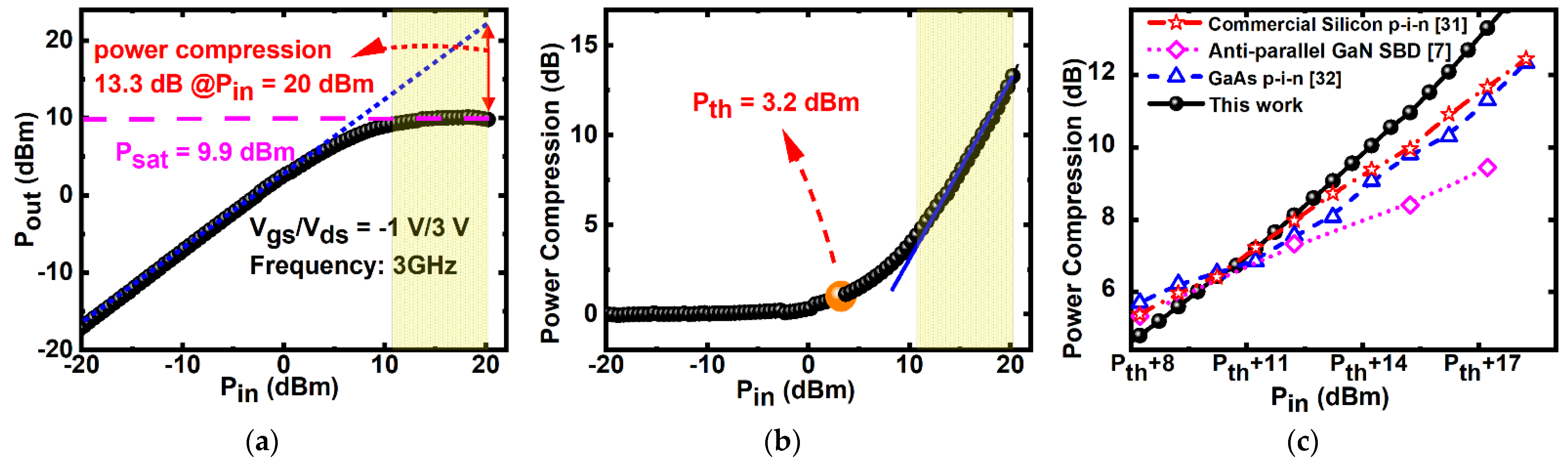
Figure 4.
(a) Pout versus Pin at different Vds; (b) transducer gain in small signal mode versus Vgs.
Figure 4.
(a) Pout versus Pin at different Vds; (b) transducer gain in small signal mode versus Vgs.
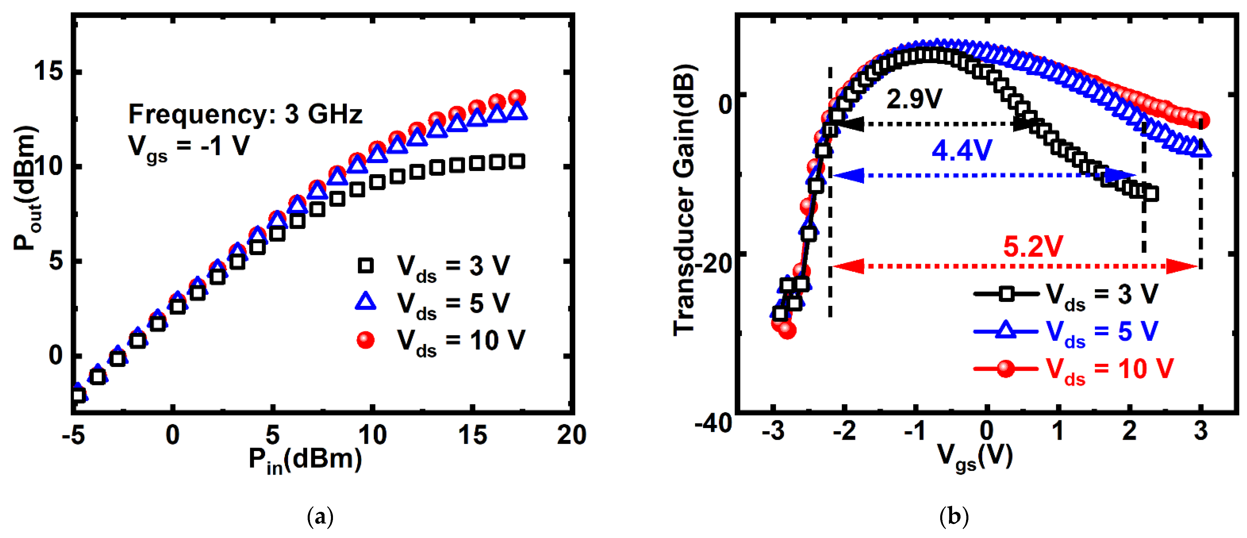
Figure 5.
(a) Pout versus Pin with 30–3000 MHz; (b) transducer gain versus frequency at Vgs/Vds = −1/3 V.
Figure 5.
(a) Pout versus Pin with 30–3000 MHz; (b) transducer gain versus frequency at Vgs/Vds = −1/3 V.

Figure 6.
(a) Phase shift versus Pin with different Vds; (b) small RF signal equivalent circuit for GaN HEMT; (c) Cgs versus gate voltage.
Figure 6.
(a) Phase shift versus Pin with different Vds; (b) small RF signal equivalent circuit for GaN HEMT; (c) Cgs versus gate voltage.
Publisher’s Note: MDPI stays neutral with regard to jurisdictional claims in published maps and institutional affiliations. |
© 2022 by the authors. Licensee MDPI, Basel, Switzerland. This article is an open access article distributed under the terms and conditions of the Creative Commons Attribution (CC BY) license (https://creativecommons.org/licenses/by/4.0/).
Share and Cite
MDPI and ACS Style
Song, W.; Guo, H.; Gu, Y.; Zhou, J.; Sui, J.; Chen, B.; Huang, W.; Zou, X. Power Compression and Phase Analysis of GaN HEMT for Microwave Receiver Protection. Electronics 2022, 11, 1958. https://doi.org/10.3390/electronics11131958
AMA Style
Song W, Guo H, Gu Y, Zhou J, Sui J, Chen B, Huang W, Zou X. Power Compression and Phase Analysis of GaN HEMT for Microwave Receiver Protection. Electronics. 2022; 11(13):1958. https://doi.org/10.3390/electronics11131958
Chicago/Turabian StyleSong, Wenhan, Haowen Guo, Yitian Gu, Junmin Zhou, Jin Sui, Baile Chen, Wei Huang, and Xinbo Zou. 2022. "Power Compression and Phase Analysis of GaN HEMT for Microwave Receiver Protection" Electronics 11, no. 13: 1958. https://doi.org/10.3390/electronics11131958
Note that from the first issue of 2016, this journal uses article numbers instead of page numbers. See further details here.