Article

An Area- and Energy-Efficient 16-Channel, AC-Coupled Neural Recording Analog Frontend for High-Density Multichannel Neural Recordings

1
College of Engineering, Electrical Information Communication Engineering, Kangwon National University, Samcheok 25913, Korea
2
College of Engineering, Electronics Engineering, Pusan National University, Busan 46241, Korea
*
Authors to whom correspondence should be addressed.
Electronics 2021, 10(16), 1972; https://doi.org/10.3390/electronics10161972
Submission received: 6 July 2021 / Revised: 10 August 2021 / Accepted: 12 August 2021 / Published: 16 August 2021
(This article belongs to the Special Issue Design of Mixed Analog/Digital Circuits)

Abstract

:
We present an AC-coupled modular 16-channel analog frontend with 1.774 fJ/c-s∙mm2 energy- and area-product for a multichannel recording of broadband neural signals including local field potentials (LFPs) and extracellular action potentials (EAPs). To achieve such a small area- and energy-product, we employed an operational transconductance amplifier (OTA) with local positive feedback, instead of a widely-used folded cascode OTA (FC-OTA) or current mirror OTA for conventional neural recordings, while optimizing the design parameters affecting performance, power, and area trade-offs. In addition, a second pole was strategically introduced in the LNA to reduce the noise bandwidth without an in-channel low-pass filter. Compared to conventional works, the presented method shows better performance in terms of noise, power, and area usages. The performance of the fabricated 16-channel analog frontend is fully characterized in a benchtop and an in vitro setup. The 16-channel frontend embraces LFPs and EAPs with 4.27 μVrms input referred noise (0.5–10 kHz) and 53.17 dB dynamic range, consuming 3.44 μW and 0.012 mm2 per channel. The channel figure of merit (FoM) of the prototype is 147.87 fJ/c-s and the energy-area FoM (E-A FoM) is 1.774 fJ/c-s∙mm2.

1. Introduction

An in-depth understanding of the brain’s activities will require large-scale recordings from multiple neuronal structures. For such large population recordings, extracellular neural recording has been recognized as one of the most powerful techniques due to its high spatial and temporal resolutions, thus, related research tools for extracellular neural recording have been steadily advanced [1,2,3]. The requirements for extracellular neural recording are high-density and high-quality signal acquisitions without unnecessary interventions for long time periods, which poses huge challenges to the engineering works for it. Those challenges when focusing on the integrated circuit design for neural recording frontends can be enumerated as follows: considering the dense population of neurons in the brain (e.g., >1000 neurons within a radius of 140 μm in the rat cortex [1]), multichannel neural recording frontend circuits that fit into a small area of the brain are highly required; due to the tiny amplitude of extracellular neural signals (~100 µV) and their high dynamic range (DR) (~60 dB), decent quality recording must be provided [4]; low-power operation of the neural recording frontends is essential because heat dissipation from the high-density neural recording frontend circuit can negatively affect living issues. As such, the requirements are not easy to achieve and are even harder when it is needed to achieve them simultaneously since they are interrelated in the context of integrated circuit design trade-offs [5]. To break the trade-offs, a lot of research into the neural recording frontend circuit design have been conducted [6,7,8,9,10,11,12,13,14,15,16,17,18,19,20,21]. Some works have accomplished an ultralow-power operation [18], others have realized the frontend circuit within a tiny area [8,19], and, recently, a few works have tried to achieve both simultaneously [9,11].
To quantitatively measure the performance of the neural recording frontend circuits, the authors of [9,10] proposed the energy-area figure of merit (E-A FoM) where the per channel energy efficiency (Channel FoM) and area consumptions of a neural recording frontend are multiplied, elucidating how efficiently a given neural recording frontend circuit uses the area and energy to provide a certain performance (smaller is better). In addition to this FoM, by referencing a few important specifications, such as input referred noise (IRN), signal-to-noise (and distortion) ratio (SN(D)R), and bandwidths, one can easily appreciate a neural recording frontend circuit compared with other similar implementations. This work, for instance, exhibits a 1.774 fJ/c-s∙mm2 E-A FoM calculated by an energy efficiency of 147.87 fJ/c-s and an area of 0.0012 mm2 per channel. The other performance indicates the channel dynamic range of 53.17 dB, IRN of 4.27 μVrms, 3.44 μW per channel power consumption with 31.25 kS/s sampling frequency. This is a decent result since it shows very small E-A FoM compared to other works (clarified later in Table 1) while satisfying the specifications for broadband neural recordings.
This work has been motivated by observing the performance of our prior works [22,23], as shown in the left of Figure 1, where a 256-channel CMOS frontend circuit (16 × 16-channel module) and the same channel flexible polyimide neural probe are combined to realize an ultrahigh-density 256-channel broadband neural recording system by using a hybrid interconnection with the anisotropic conductive film (ACF). In [22,23], to be flip-chip bonded with a flexible neural probe, a low noise amplifier pixel (+buffer) was buried under the area pad with a tiny pitch of 75 μm, eliminating input pads in the chip perimeter. Though successful, the essential circuit performance, such as IRN and power consumption were compromised due to the restricted area. Thus, this work primarily focuses on how to achieve better IRN with smaller power consumption, while inheriting the same pixel pitch and reducing the area consumption further by introducing novel circuit design techniques.
This paper is organized as follows: The overview of the AC-coupled 16-channel neural recording frontend and details of the area-aware design applied for the low noise amplifier pixel and its consequent benefits are provided in Section 2. The modification of the pixel structure to further save the area consumption is also given in the same section. Then, the measurement results from the benchtop and in vitro set-up, and the comparison of the measured performance with other recent state-of-the-art works are presented in Section 3. Finally, Section 4 concludes this paper.

2. A 16-Channel, AC-Coupled Analog Frontend

Analog frontend integrated circuit architectures for neural recordings to achieve a decent performance while maintaining the balance between power and area consumptions have, recently, been extensively researched. As summarized in [11], one can roughly classify these into the three distinct circuit architectures: (1) AC-coupled amplifier and analog-to-digital converter (ADC), (2) DC-coupled amplifier and ADC, and (3) DC-coupled direct ADC. The first architecture may be one of the most popular and widely adopted topologies [4,6,10,24,25,26,27]. It provides a decent and balanced performance in terms of noise, gain uniformity, distortion, and so on, while consuming relatively high power and large area [6]. The DC-coupled amplifier and ADC architecture was introduced to reduce the area consumption by eliminating bulky input coupling capacitors in the AC-coupled architectures, but it needs the extra area and power for the mixed-signal feedback loop which it must have [8,19]. The DC-coupled direct ADC has been introduced most recently. The frontend Δ-modulation and switched capacitor-based sampling [28], and the difference-differential input stage-based Δ-modulation [29] can achieve a rail-to-rail input range, but these cost a high oversampling rate, limiting their applications to low frequency neural signals, such as electroencephalogram (EEG), intracranial EEG, local field potential (LFP), and electrocorticogram (ECoG). In this work, the conventional AC-coupled architecture has been chosen to inherit its advantages over the newly developed architectures, such as excellent gain uniformity across the multiple channels, less design effort due to the well-developed design procedures, inherent passive offset cancellation, and relatively high input impedance, while compensating the high power and large area consumptions with the proposed novel circuit design techniques.

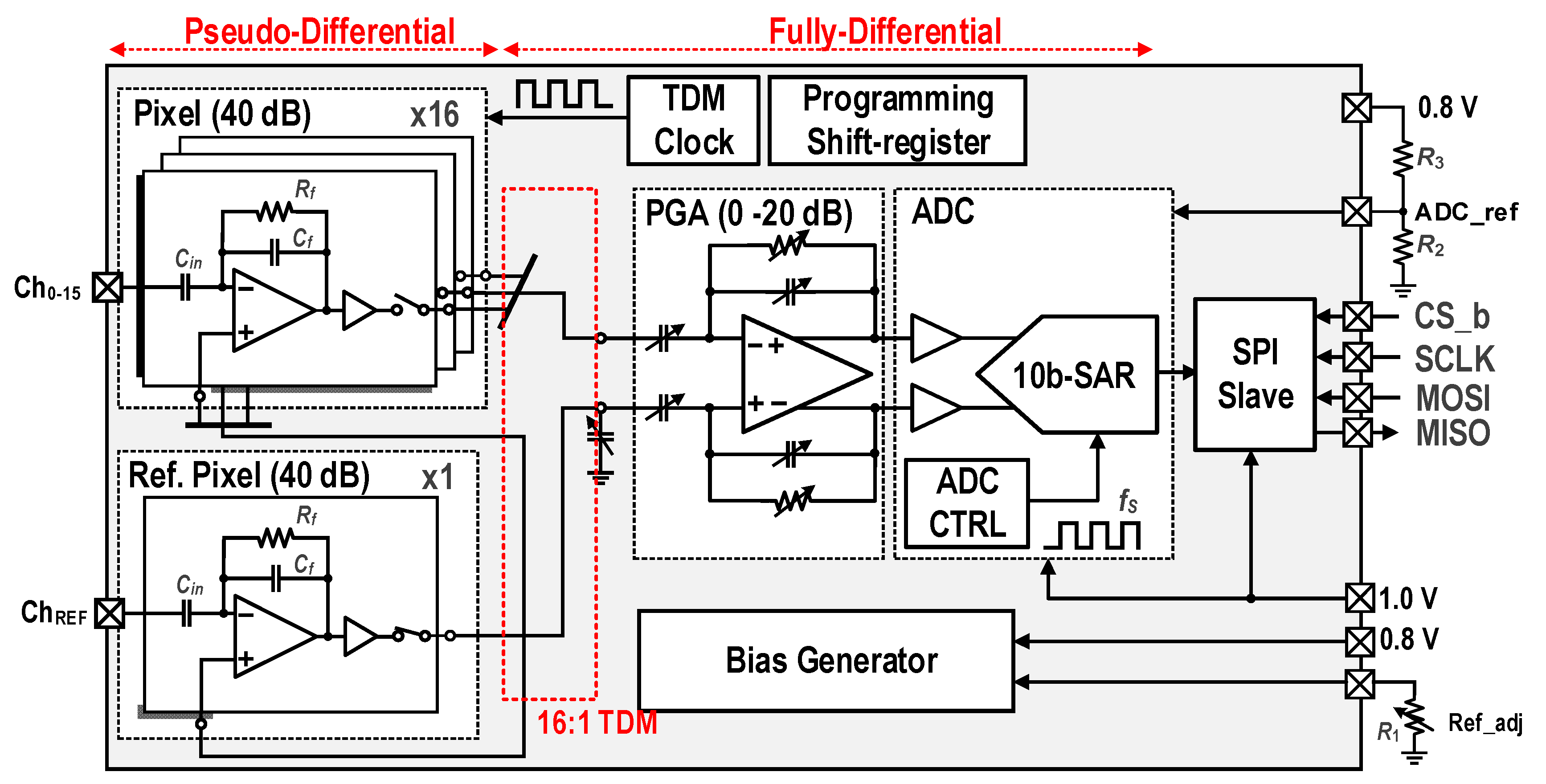
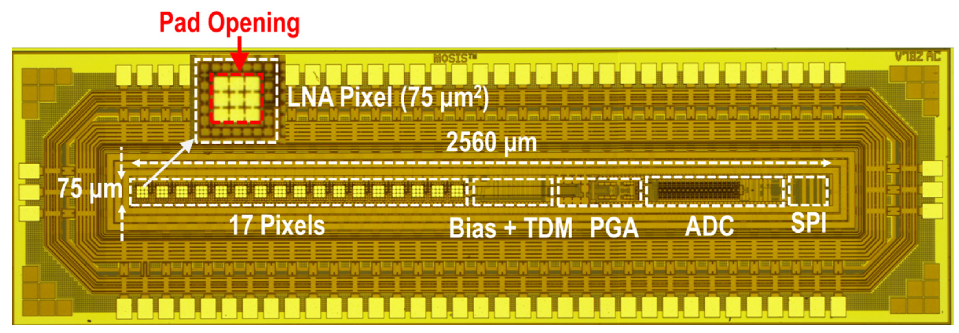
2.1. Integrated Circuit Architecture

Our 16-channel, modular and expandable architecture is shown in Figure 2. It consists of 17 low noise amplifiers (LNAs) and time-division multiplexing (TDM) buffers, a TDM switch array, a programmable gain amplifier (PGA), a successive approximation register (SAR) analog-to-digital converter (ADC), and a serial peripheral interface (SPI). All voltage and current references are internally generated. To save area, the pixel is implemented with single-ended input and output, resulting in half-size passives of the conventional AC-coupled structures [22,23]. The multiple input signals are coupled into the single-ended input and output LNAs, which does not have any common mode (CM) rejection, but this is compensated by the replica reference where the exact same LNA accepts the reference signal, as shown in Figure 2 (left). Thus, the input and reference paths have the same impedance (Zin = Zref), rejecting CM signals in a pseudo-differential manner. After the initial amplifications, the buffers drive the TDM switches and parasitics; then, the PGA provides further gain according to experimental environments. The SAR ADC quantizes the output of the PGA and loads the data in accordance with the format of the SPI.

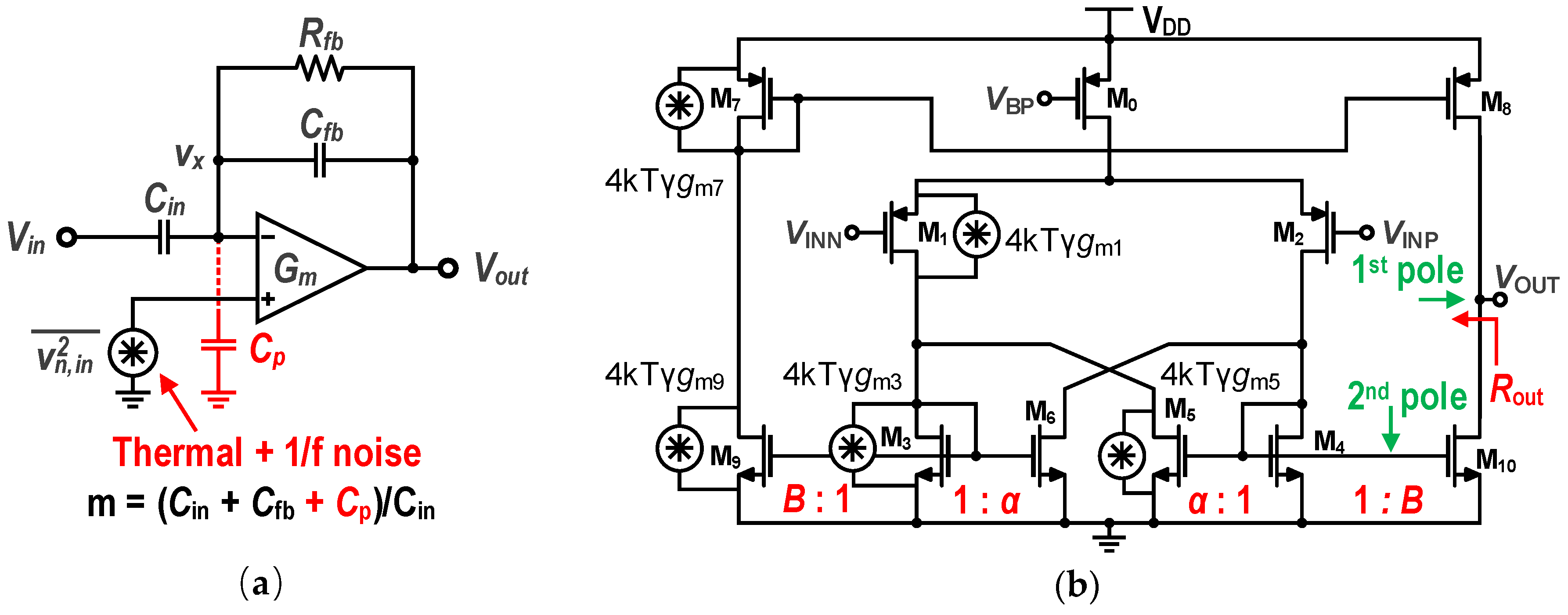
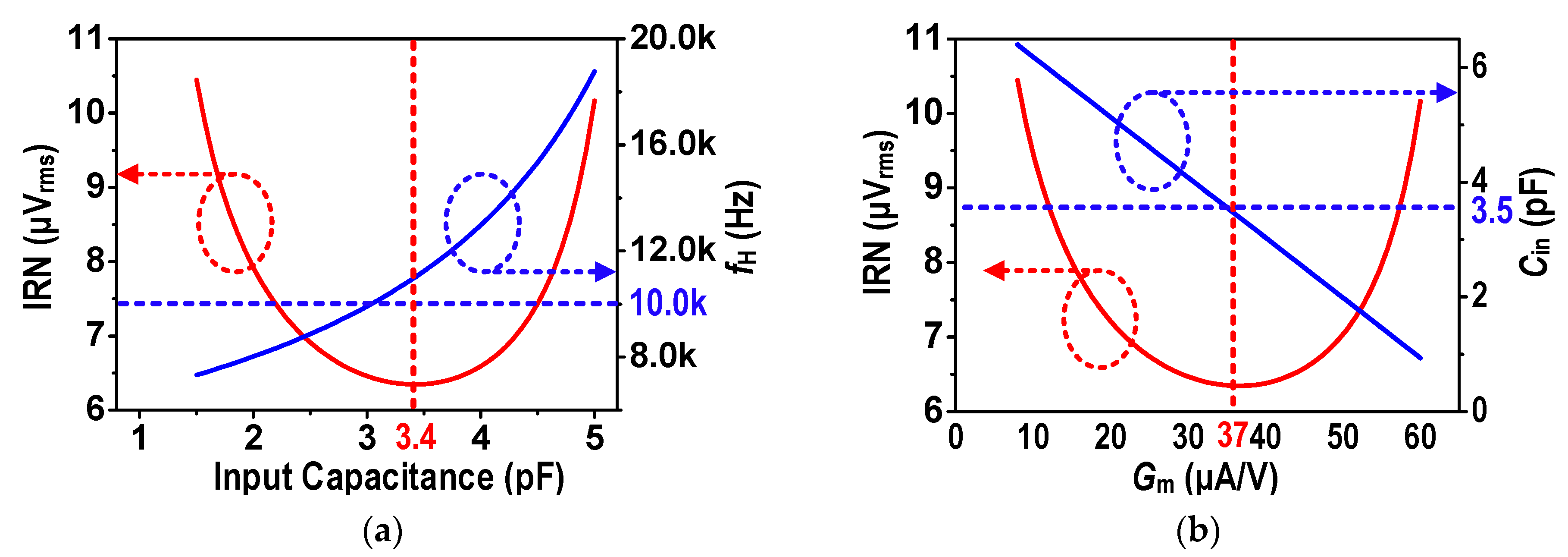
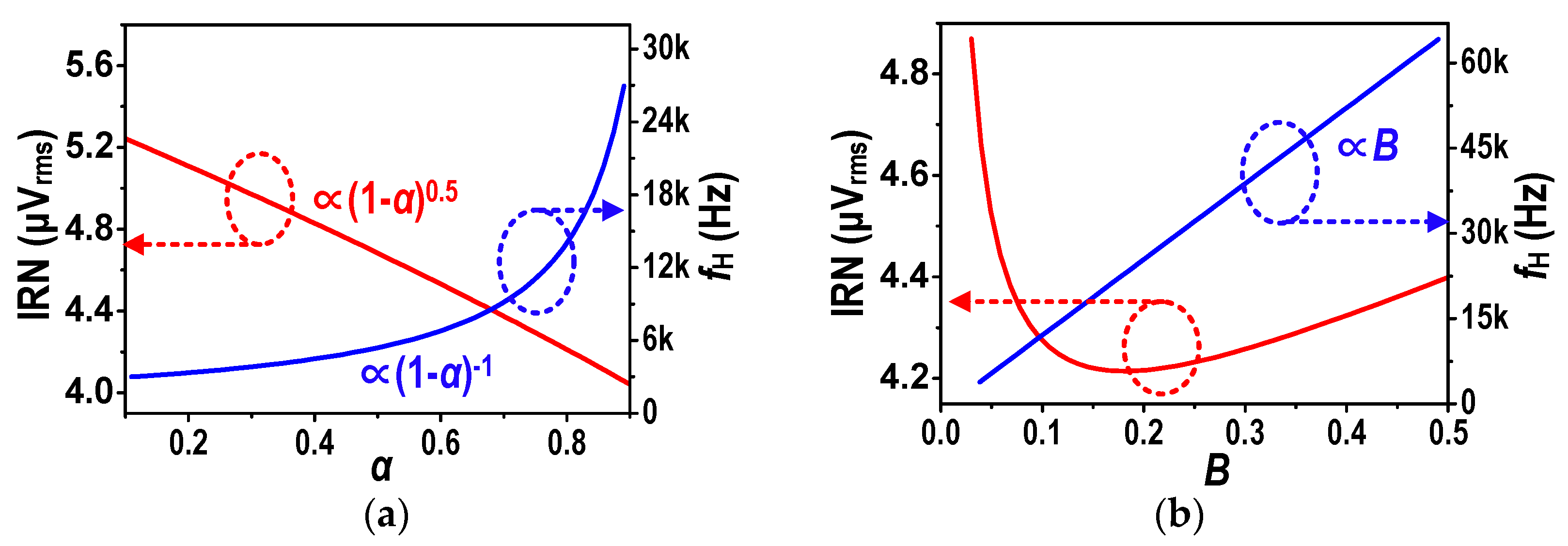
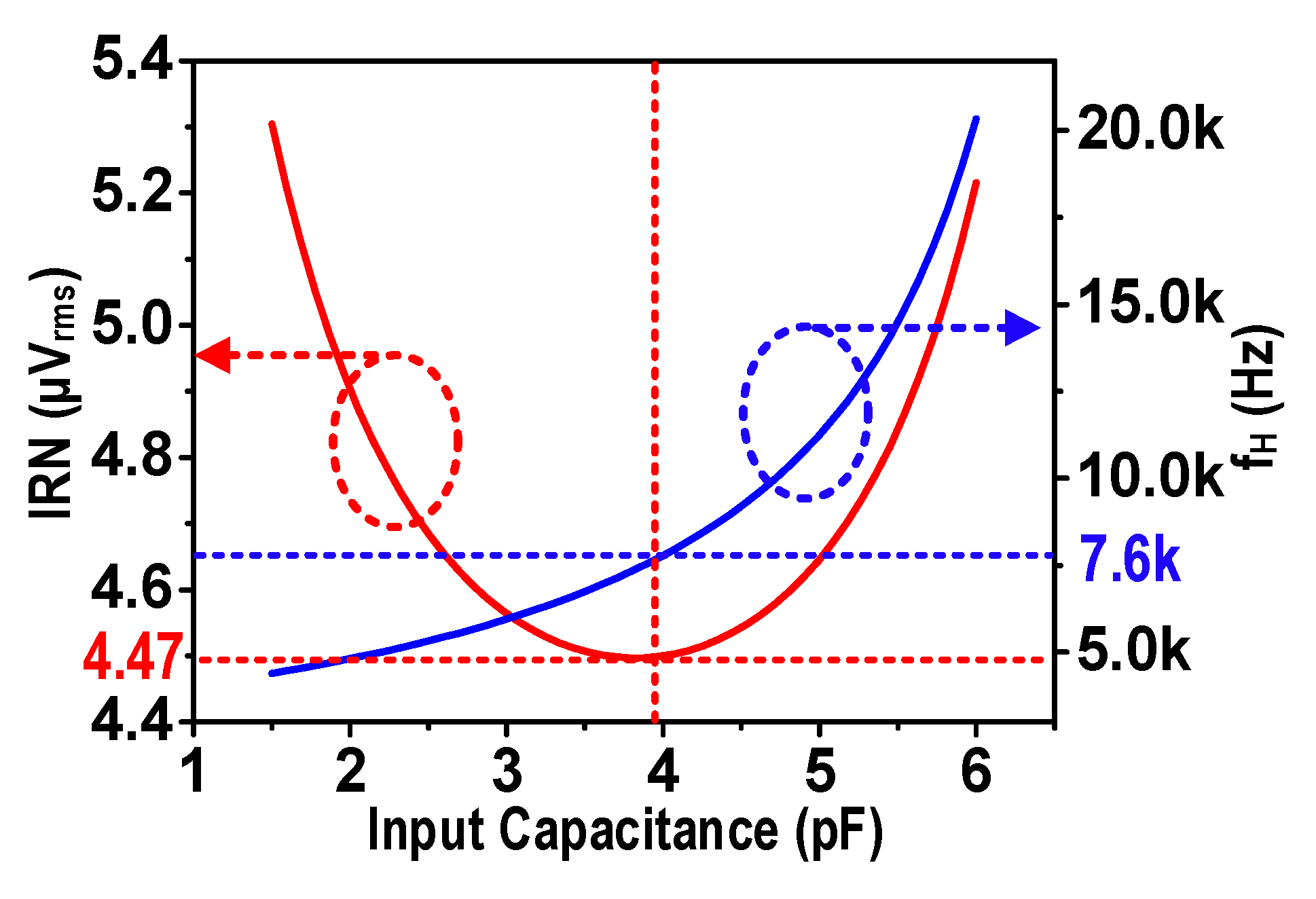
2.2. Area-Aware Design in Low Noise Amplifier

The key innovations of this work lie in the pixel circuit design (an LNA + a buffer), which improves noise power performance with the given area of 75 μm2. The previous work in [22,23] also accomplished the same size pixel; however, it showed a relatively high IRN of ~6.3 μVrms due to the limited space while consuming a relatively large power consumption (~8.9 μW). In this work, we realized a smaller IRN and power consumption of the same size thanks to the area-aware design techniques and the adoption of an operational transconductance amplifier (OTA) with a local positive feedback.
A design methodology considering the area consumption in an AC-coupled LNA was introduced in [30]. While assuming that the area consumption is dominated by passive components in an AC-coupled amplifier, the area (A) required for a differential AC-coupled LNA is given by
A = C L + 2 C i n + 2 C f C d = C L + 2 ( A M + 1 ) C f C d
where Cin, Cf, and CL are the input, feedback, and load capacitance, respectively, Cd is the capacitor density in a chosen technology node (usually, 1 − 4 fF/μm2), and AM is the mid-band gain of the AC-coupled amplifier (=Cin/Cf). In addition, the power of the input referred noise and noise bandwidth (NBW, Δf) are given as:
v n i , t h 2 _ 16 k T 3 G m Δ f
Δ f = f H π 2 = ( G m 2 π C L 1 A M ) π 2 = G m 4 C L A M ,
respectively, where k is the Boltzmann constant, T is the absolute temperature in Kelvin, and Gm is overall transconductance of the amplifier in use. Since CL affects Δf and the power of the input referred noise must be calculated using Δf, the two Equations (2) and (3) are combined and then plugged into Equation (1)
A = 4 3 k T v n i , t h 2 _ A M C d + 2 ( A M + 1 ) C f C d
By using Equation (4) one can design an area-optimized, AC-coupled LNA while maintaining decent IRN performance. In general, this equation makes sense, however, it has limitations; this equation disregards one of the major noise sources in the AC-coupled LNA: flicker noise (or 1/f noise) and the noise multiplication (m = (Cin + Cf + Cp)/Cin, Cp: input parasitic capacitance); thus, it results in a sub-optimal design. While it may be fine when there is enough space to implement large input transistors to minimize 1/f noise (if that is the case, the portion of the 1/f noise in the total IRN of the broadband neural recording amplifiers (1–10,000 Hz) is usually ~10% [6]), it cannot be neglected in the designs where the optimal usages of the area and power is highly required, particularly when the given area is too small to allocate enough space for the input transistors. In addition, the absolute values of the passives, Cin and Cf, cannot be set large if the given area is small, therefore, m is easily and negatively affected by large Cp. Including the above discussions and considering that the LNA has a single input and output as in our approach, as shown in Figure 3a, Equation (4) is modified as
A = 4 3 m 2 k T v n i , t h + 1 / f 2 _ A M C d + ( A M + 1 ) C f C d
According to [30], Equation (1) tells us that the optimal IRN and the optimal AM (AMopt) would be given by varying AM, however, the suggested optimization process is not likely to produce the best result for the design for circuit blocks after the LNA because small AM incurs design penalties, such as higher noise or higher power consumption in the following blocks. Therefore, it seems to be more appropriate to fix AM. We set AM as 100 by assuming a smaller Cfb than that provided by the given process (~35 fF), which is realizable by using a capacitor T-network to some extent [25]. In addition, we calculated the amount of capacitance we can use in the given area. With the consideration of the given area of 75 μm2, the capacitor density (Cd = 2 fF/μm2), and design rules of the selected 180 nm CMOS process, ~9 pF metal-insulator-metal (MIM) capacitance is readily available.
We then performed numerical simulations to observe the trade-offs given by Equation (5). Figure 4a shows the IRN and high frequency cutoff (fH, proportional to Δf) of an LNA by sweeping Cin with the given total usable capacitance (Cusable ~9 pF). For the simulation, a source degenerated folded cascode operational transconductance amplifier (FC-OTA) with a few μA of current consumption was selected for the open-loop-amplifier [24,31]. As Cin decreases, fH monotonically increases due to the smaller CL (CL = CusableCinCfb), while the optimal IRN can be found due to larger noise bandwidth as Cin increases (to the right), and by larger noise multiplication (m) as Cin decreases (to the left). As opposed to a common belief in the tradeoff between power consumption and noise, a larger power consumption would not be helpful if the implementation area were fixed due to the increased NBW. Another numerical simulation in Figure 4b clearly shows this. This simulation predicts how much power must be burned to achieve the smallest noise with the given area constraint. In this case, Cin becomes smaller as Gm increases since we fixed fH as 10 kHz, thus, CL must be increased. The IRN increases as Gm decreases, according to Equation (2); the opposite can happen due to a higher m by smaller Cin. Without our modification in Equation (4), both gradient descent points in Figure 4 for the IRN may not be found.
As predicted in Figure 4, due to the fundamental relationships between Gm and fH (or Δf), assuming that the OTA is a first order system, i.e., the linear proportionality of fH to Gm, given by Equation (3), and between thermal noise power and Gm, the implementation of an AC-coupled neural recording amplifier with decent IRN (<5 μVrms) looks very hard to achieve with the given small area of 75 μm2. This is evident if recalling our previous LNA based on FC-OTA implementation [22] that was designed in accordance with the described design flow with the same size of 75 μm2 and showed a slightly high IRN of >6 μVrms despite a relatively high power consumption of ~8.9 μW (~7.4 μA current).
Based on the previous discussions, to achieve smaller IRN with the given implementation area, the fundamental relationship between Gm and Δf must be broken. In this paper, we adopted a different type of OTA, as shown in Figure 3b, whose Gm can be weakly coupled to IRN and Δf through the proper selection of the design parameters. The OTA in Figure 3b uses a local positive feedback with M5,6 and an additional current gain with M9,10 to boost the overall Gm
G m = g m 1 B 1 α
where gm1 is the transconductance of the input transistor, M1,2, α and B are the ratios of the geometries of M6 to M3 and M3 to M9, respectively. The output referred noise (ORN) and IRN of the OTA are given as
v ¯ n , o u t 2 = 8 k T γ [ ( g m 1 + g m 3 + g m 5 ) B 2 + ( g m 7 + g m 9 ) ] R o u t 2
v ¯ n , i n 2 = 8 k T γ ( 1 α ) 2 g m 1 ( 1 + g m 3 + g m 5 g m 1 + g m 7 + g m 9 g m 1 B 2 )
where Rout is the output impedance of the OTA and γ is a constant for the transistor channel noise. Unlike the conventional design of the chosen OTA where α < 1 and B > 1 for a stable positive feedback with Gm boosting [32], we selected α < 1 and B < 1 to suppress the noise bandwidth, Δf, while achieving decent noise performance. According to the last term in Equation (8), once B has been selected to be less than 1, B2 inevitably increases IRN. However, in this case its effect would be minute, because gm7,9 and gm9 are usually very small compared to gm1 to minimize power consumption and that no high slewing is required for neural recording applications. We also performed numerical simulations to demonstrate this. As shown in Figure 5a, the IRN is proportional to (1 − α)0.5. This relationship comes from the fact that the proportionalities in the power spectral density (PSD) of the IRN to (1 − α)2 and fH, i.e., Δf to (1 − α)−1. Figure 5b depicts the effect of B for fH and IRN. The IRN quickly increases due to the proportionality of the PSD of the IRN to B−2, according to (8) as B decreases. On the other hand, the IRN is also increased by the higher fH as B increases. Since the fH should be set not only by considering the IRN but also by the general specification for neural recordings, α = 0.7 and B = 0.1 were selected. Based on the parameters in Figure 5, we designed an AC-coupled neural recording amplifier within 75 μm2 of area. Figure 6 shows the IRN and fH versus Cin with the selected topology. It shows the similar optimal point in Figure 6, while showing the better noise performance of 4.47 μVrms.

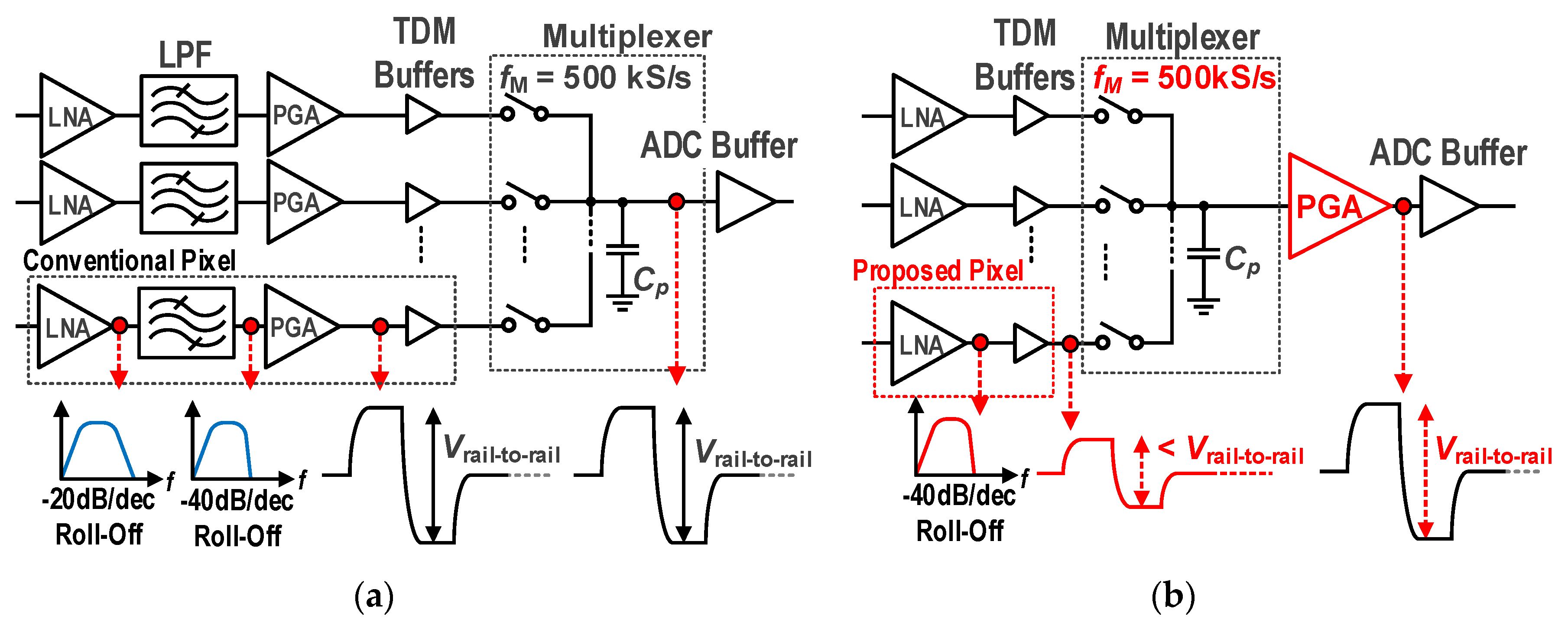
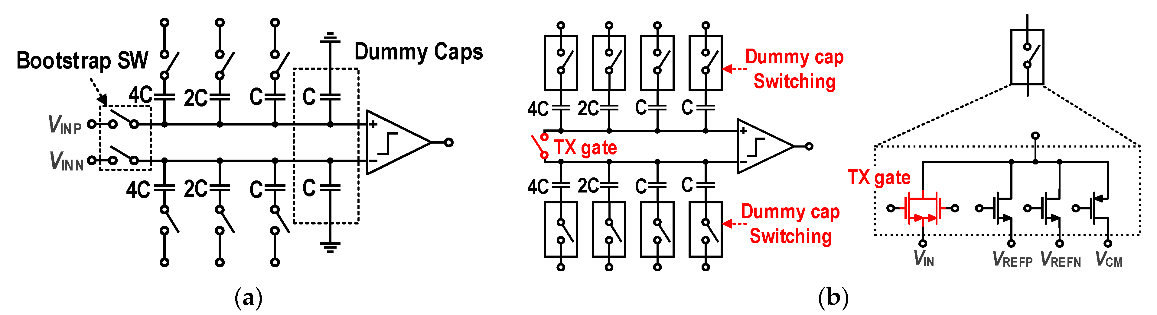
2.3. Improvement in Pixel Structure

A typical pixel circuit block in time-division multiplexed multichannel recording architectures consists of a low noise amplifier, buffer, programmable gain amplifier (PGA), and a low-pass filter (LPF), as shown in Figure 7a [33,34,35]. In the proposed 16:1 TDM architecture, two major improvements for smaller area and power consumptions were made, as shown in Figure 7b. First, as opposed to the conventional pixel structure where the additional LPF after the LNA realizes fast roll-off in the high-frequency region to reduce noise aliasing in the TDM, ~−40 dB roll-off is implemented in the LNA. A well-designed OTA can be regarded as a first order system and its phase margins is ~90° when configured in a feedback network because the second pole (P2) is usually located at a higher frequency than that of the dominant pole (P1), as indicated with the black lines in Figure 8a. However, in the neural recording, LNA, which has a high closed loop gain (~40 dB), in other words, a small feedback factor (β) and operates in a pure continuous time domain, such a high phase margin is unnecessary, ~60° of phase margin would be enough [30,36]. Therefore, the early introduction of the second pole (P2’ indicated in red), which reduces some phase margin, does not negatively affect the loop stability. Instead, it provides faster roll-off and, thereby, no additional LFP is required in the pixel structure. The top of Figure 8b shows the simulated Bode diagram (gain and phase) of the proposed OTA. As shown, the phase margin when the open-loop gain crosses a 40 dB (=1/β) line is >80°, indicating the closed loop operation is stable. The bottom of Figure 8b shows the simulated close loop gain of the proposed LNA. Thanks to the early introduction of the second pole, it has faster high-frequency roll-off without the aid of an additional LPF.
In addition, the in-channel PGA has been moved after the analog multiplexer to avoid the slew-limit operation in the TDM buffer [23]. Thanks to such a modification, the buffer can be designed considering only the linear settling. This configuration also helps the neural recording frontend save power and area. As depicted in Figure 7a, in the conventional design, the output of the in-channel PGA is almost rail-to-rail to maximize signal DR. Thus, the following TDM buffer must be designed by considering the slew-limiting operation, which results in high power consumption. On the other hand, by placing the PGA after the multiplexer, the input range of the TDM buffer becomes smaller, estimated as ~200–300 mVpp at best (considering the maximum LPF amplitude of ~3 mV); in other words, the buffer can be designed by only considering linear settling.

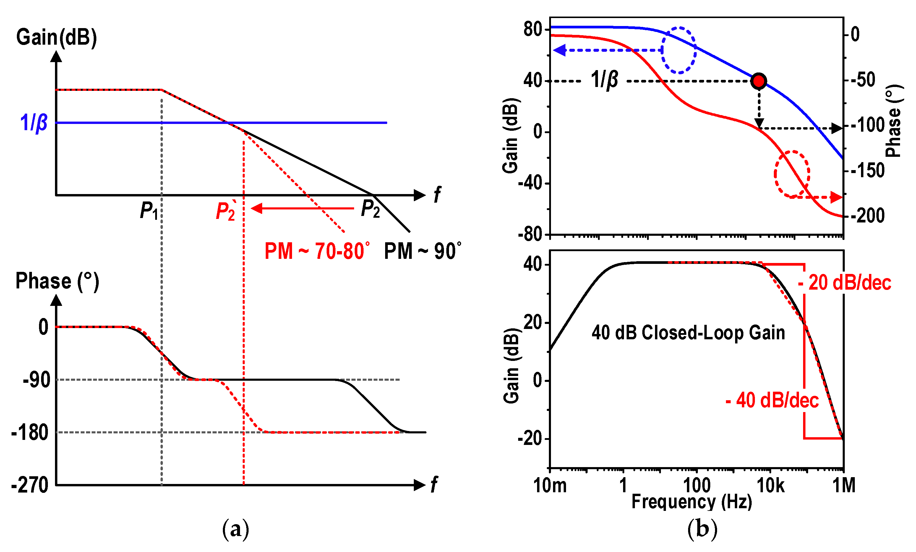
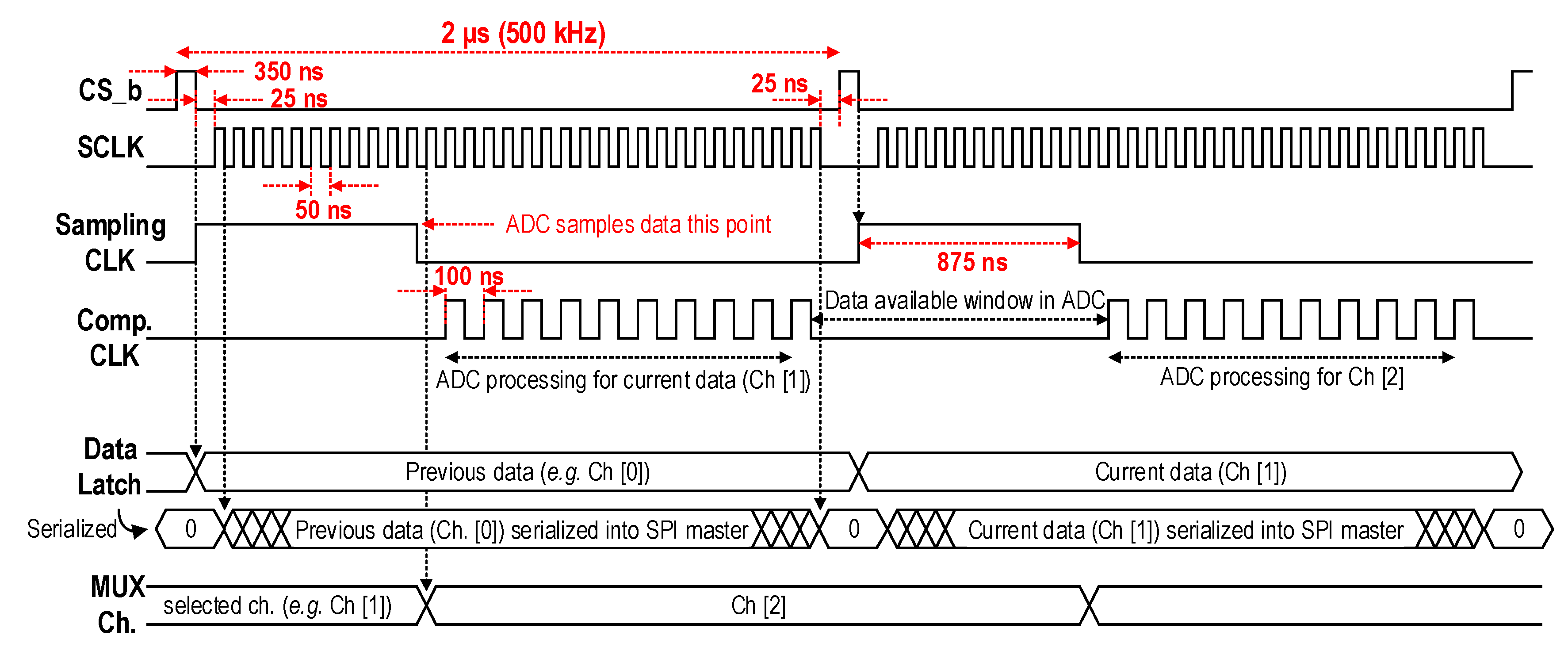
2.4. Analog-to-Digital Converter and Serial Peripheral Interface

The design of the SAR ADC used in this work has been adopted from [22,23], thus, let us briefly explain the technique in this paper here. The fully differential 10b SAR ADC is implemented with a smaller area by reducing the size of capacitor DAC (CDAC) by half compared to the conventional top plate sampling CDACs. With a conventional top plate sampling, a 4-bit resolution can be achieved with a total 16C (=4C + 2C + 1C + 1C and differential, where C: unit capacitor), which has a 2× smaller capacitor with the aid of the bootstrap switches when compared to a 4-bit bottom plate sampling CDAC, as shown in Figure 9a. In this implementation, an additional 2× smaller CDAC has been achieved by the introduction of the dummy capacitor switching technique as shown in Figure 9b, resulting in a 5-bit resolution with the same capacitor size as that in Figure 9a. Thus, for a 10-b differential DAC, 512C is sufficient. In addition, in this implementation the input signal is sampled via a simple transmission gate (TX gate) via a switch that shorts the top plates without the bootstrap switches. For energy-efficient operation, we adopted a VCM-based switching technique [37], therefore, four switches are required for a unit capacitor as shown in the right of Figure 9b. The overall sampling capacitor is ~4.48 pF for fully differential operations. All switches and active components are buried under the MIM capacitors to further save area consumption. By applying the VCM-based switching and terminating capacitor switching scheme, we implemented the fully differential 10b SAR ADC in a small area of 75 × 350 μm2 and power consumption of ~6.02 μW at its full speed of 500 kS/s, equivalently ~0.377 μW per channel.
Figure 10 shows the timing diagram of the implemented SPI slave. One SPI cycle is 500 kS/s and includes 32 SCLKs. To relax the driving requirement of the SAR ADC and TDM buffers, 0.875 and 2 μs are assigned for the settling time. The data from the SAR ADC is once latched and then serialized onto MISO (master-in, slave-out) signal. The SPI slave is implemented with the standard cells provided by the chosen 180 nm CMOS technology and auto placement and routing (APR) in an area of 75 × 450 μm2.

3. Experimental Results

The prototype 16-channel AC-coupled neural recording analog frontend chip was fabricated using a 180 nm 1P6M CMOS process. Figure 11 shows a microphotograph of the fabricated prototype chip. One of the pixels is enlarged and attached as a subset in Figure 11, clearly indicating the pad opening for the later flip-chip bonding with a neural probe using ACF. Thus, except for a few pads for 0.8 V analog and 1.0 V digital supplies, ground, and SPI controls, the pads are only for the benchtop characterization. The active area of the chip occupies 2.56 × 0.075 mm2. The important functional blocks, such as the pixels, PGA, ADC, SPI, and bias block, are highlighted.

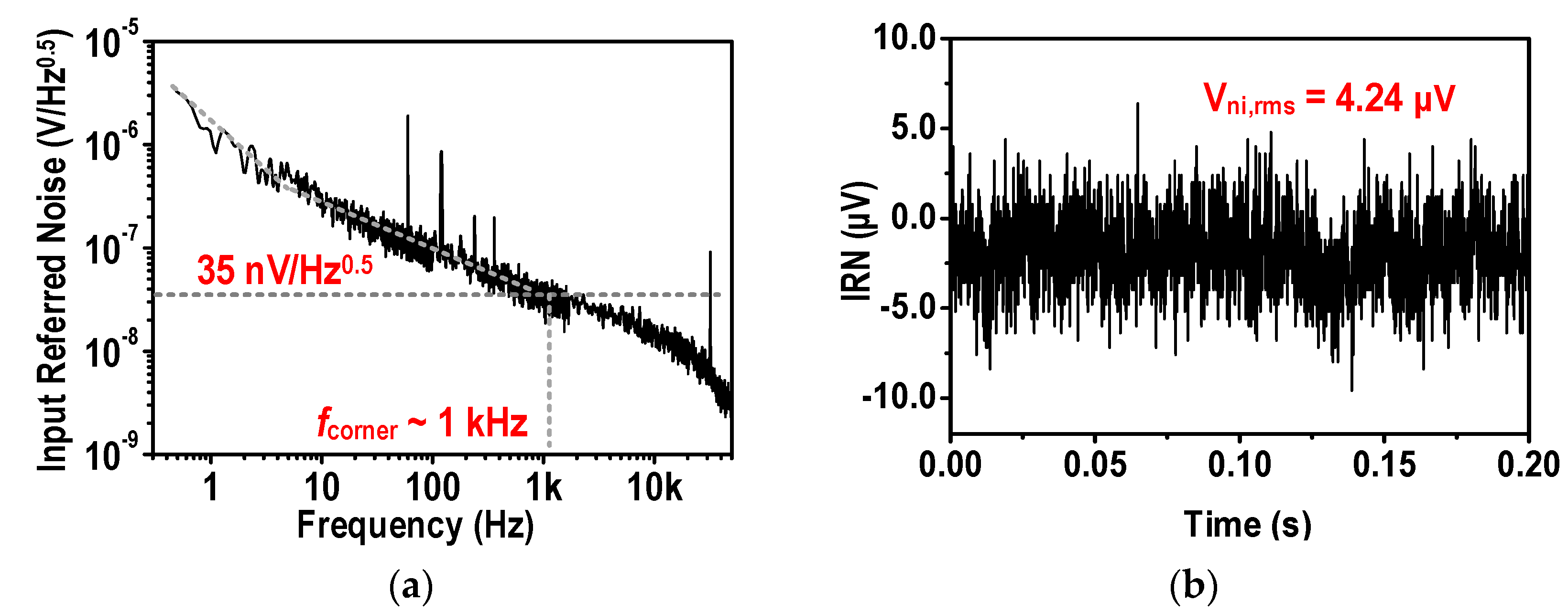
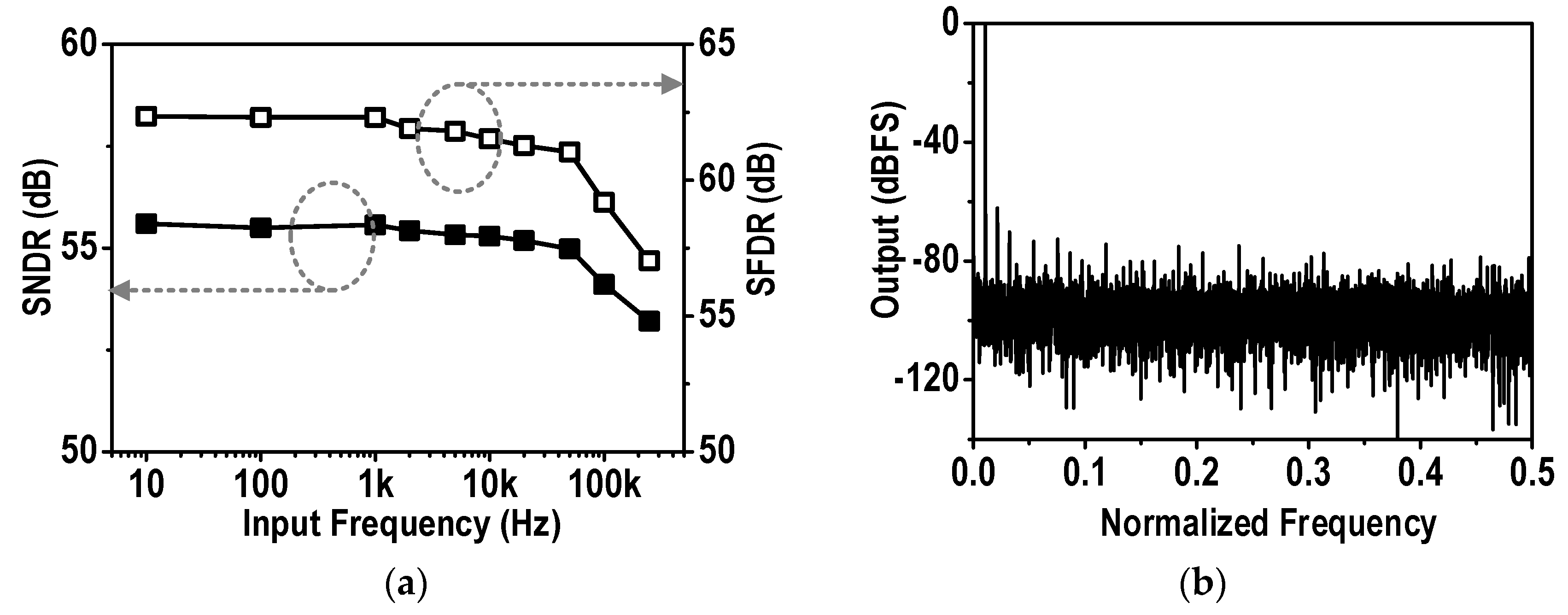
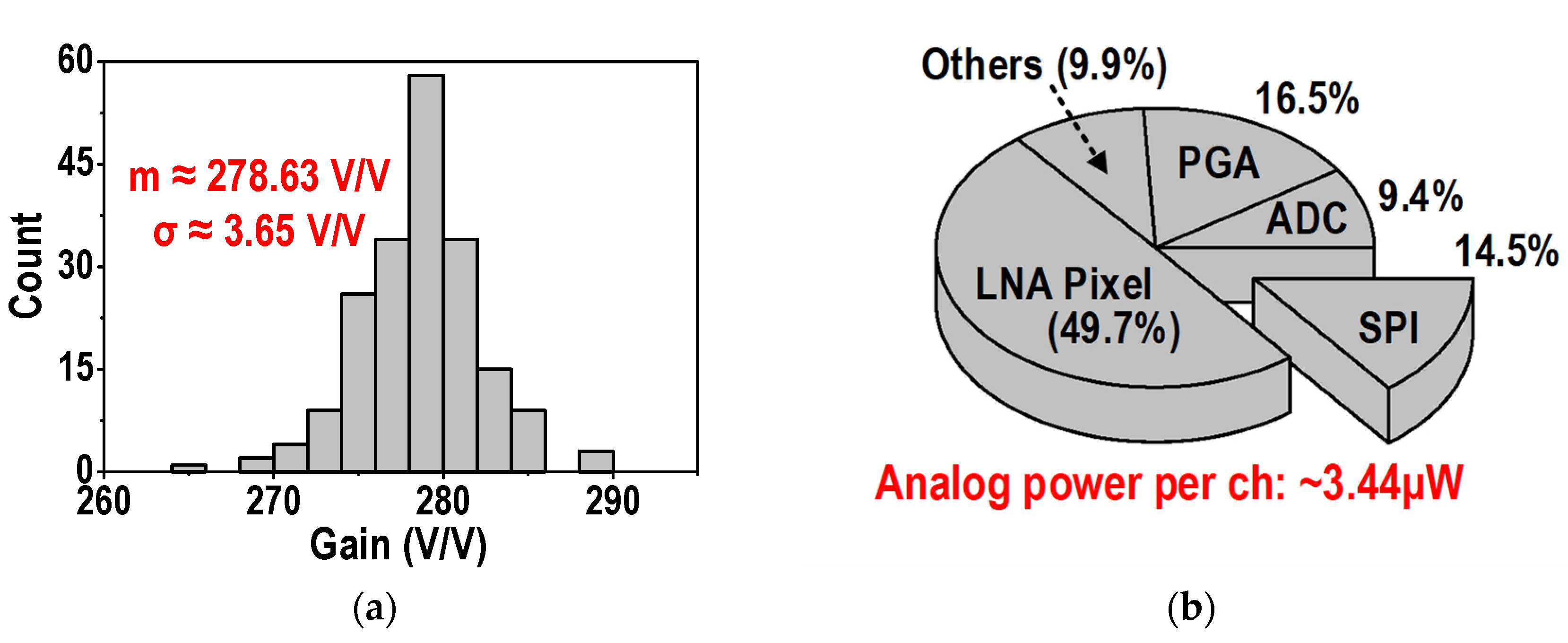
3.1. Benchtop Characterization

Figure 12a shows the frequency response of the fabricated LNA measured with a spectrum analyzer (35670A, Keysight). The mid-band gain was measured as 40 dB and its low (fL) and high (fH) frequency corners were 0.1 Hz and 7.4 kHz, respectively. The −20 dB/dec slope was observed near fH and the roll-off soon became −40 dB/dec thanks to the early introduced pole. The total harmonic distortion (THD) was also measured by varying the input amplitudes of a 1 kHz sinewave as shown in Figure 12b. This shows <1% THD when the input signal was less than 8.6 mVpp. The relatively large input amplitude with <1% THD can be achieved thanks to the reference-replica technique that forms a differential-difference amplifier structure.
Figure 13a,b show the noise measurements using a spectrum analyzer (35670A, Keysight, Santa Rosa, CA, USA) and an oscilloscope (MSO2004B, Tektronix, Santa Rosa, CA, USA), respectively. Figure 13a depicts the spectrum of the IRN from 0.4 Hz to 50 kHz. The noise floor and the 1/f corner were ~35 nV/√Hz and ~1 kHz, respectively. The total integrated IRN was calculated as 4.27 μVrms from 0.4 Hz to 50 kHz, which shows a good agreement with the transient noise measurement as shown in Figure 13b. In the transient noise measurement, 5 seconds of data was collected with a sampling rate of 12.5 MS/s. The ADC was also characterized in the benchtop. Figure 14a shows the signal-to-noise and distortion ratio (SNDR) and signal to spurious-free dynamic range (SFDR) according to the range of the input frequency from 10 Hz to the near Nyquist rate (249 kHz). Both the SNDR and SFDR begin to be degraded for >50 kHz input frequencies but still show decent performance. Figure 14b demonstrates one example of the fast Fourier transform (FFT) when the input frequency is 5 kHz. The calculated effective number of bit (ENOB) is ~8.9 bit at 1 kHz input sinewave.
The measured differential nonlinearity (DNL) and integral nonlinearity (INL) of the 10-b SAR ADC are distributed at +0.15/−0.35 and +1.75/−2.15, respectively. Figure 15a shows a gain distribution of an entire analog frontend channel including LNA and PGA with a 9 dB gain setting. The mean value of the channel gain is ~278.63 v/v (nominal value: 40 dB + 9 dB ≈ 281.84 V/V) with a standard deviation of ~3.65 v/v among 12 different samples. The variations for the IRN, fL, and fH are also measured as ~4.2 ± 0.08 μVrms, ~0.097 ± 0.0038 Hz, and ~7.4 ± 0.06 kHz, respectively. The relatively high variation in fL (~8%) may come from the pseudo-resistor formed by the near-off transistors, but such variation may be fine for the neural recordings since it is low enough to embrace the LFPs. Figure 15b shows the percentile of the power consumption of each block. The power consumptions per channel are ~3.44 and ~0.58 μW from a 0.8 V analog and 1.0 V digital supplies. The LNA that determines overall noise performance consumes the largest portion of power of ~2 μW.

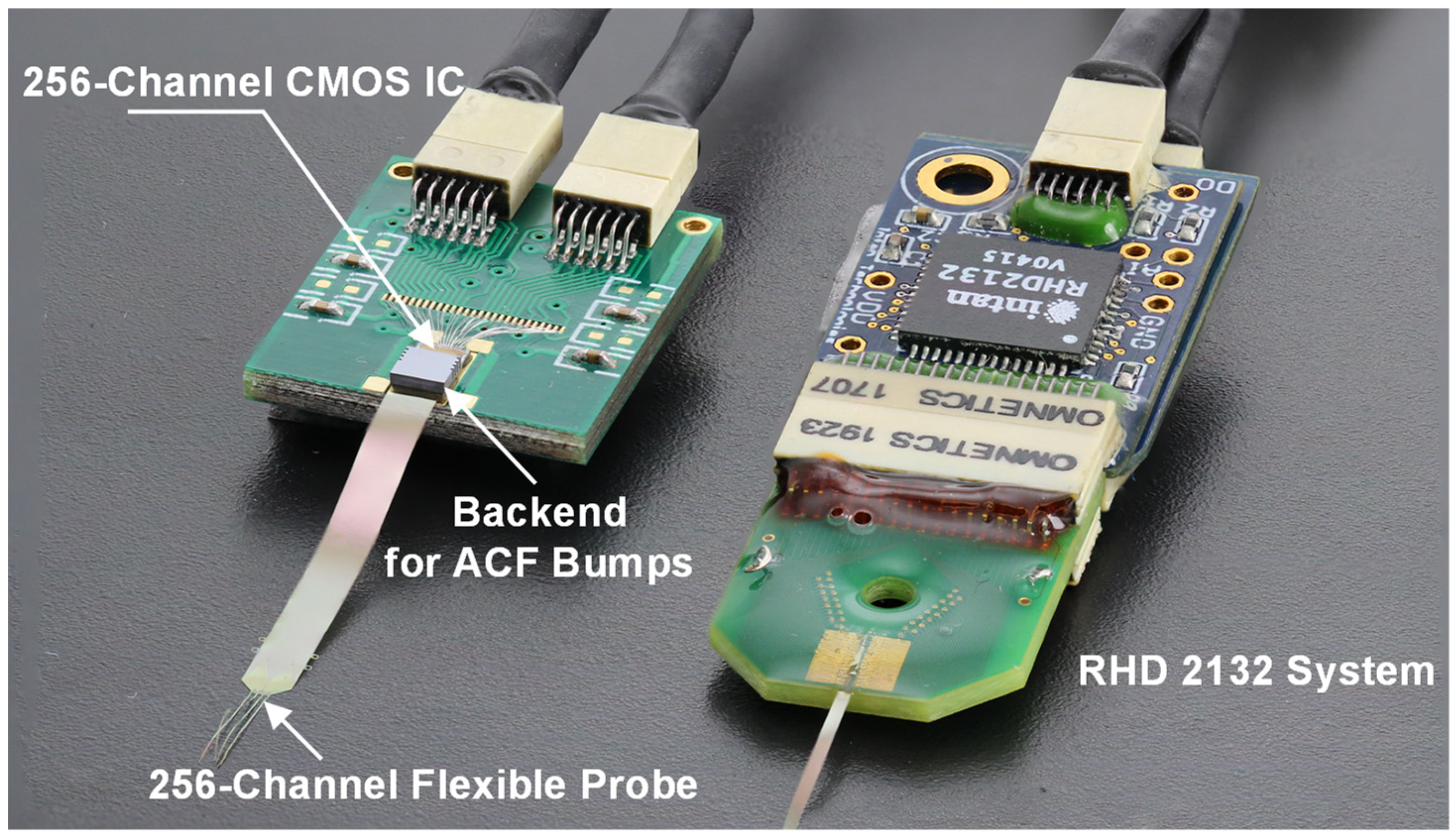
3.2. In Vitro Characterization and Performance Comparison

To further characterize the functionality of the fabricated 16-channel AC-coupled neural recording frontend, we performed measurements in phosphate buffered saline (PBS) by applying a set of pre-recorded neural data including LFP and EAP signals. The measurement was performed with the gain of ~280 v/v (40 dB from the LNA, 9 dB from the PGA) and the circuit was battery-powered. The data were collected in real-time by a custom software (LabView, National Instrument). The top and bottom of Figure 16 shows the input referred neural signals including LFP and EAP (spike) and the software (MATLAB, MathWorks) bandpass filtered (fL = 250 Hz and fH = 7.5 kHz) spikes, respectively.
The performance of this work is compared with recent state-of-the-art works in Table 1. This work shows a decent channel FoM and E-A FoM of 147.87 fJ/c-s and 1.77 fJ/c-s∙mm2, respectively, while some essential performance for neural recordings, such as the bandwidth and IRN, are comparable or better than other recent works. Particularly, this work shows the smallest footprint of 0.012 mm2 per channel except for that in [11]. While [11] considers only the active circuits into their estimation, this work takes the active circuits and LNA input pads that will be coupled to a neural probe into consideration, thus, this work could use the area more effectively than [11]. This is of particular importance in multichannel neural recording systems with a high count because the overall chip area is ultimately limited by the interconnection with neural probes, not active circuits when the channel count becomes large [23].

4. Conclusions

In this paper, we present an energy- and area-efficient AC-coupled 16-channel analog frontend for multichannel recording of broadband neural signals. To achieve such a small area- and energy-product, we devised an improved area-aware design, especially useful for very area-constrained neural recording LNA designs, and employed an OTA with a local positive feedback with the differentiated design parameter selection, while optimizing the design parameters affecting performance, power, and area trade-offs. In addition to that, a second pole was strategically introduced inside the LNA to reduce the noise bandwidth without an in-channel low-pass filter to further save the area and energy consumption. Therefore, compared to our previous work and other conventional works, the presented prototype shows better performance in terms of noise, power, and area usages. The prototype fabricated in 180 nm 1P6M CMOS process consumes 3.44 μW and 0.012 mm2 per channel while achieving the IRN of 4.27 μVrms with a channel and E-A FoM of 147.87 fJ/c−s and 1.77 fJ/c−s∙mm2, respectively.

Author Contributions

Conceptualization, Y.P. and S.-Y.P.; methodology, H.-J.K. and K.E.; software, S.-Y.P., Y.P. and K.E.; validation, H.-J.K. and S.-Y.P.; formal analysis, Y.P. and H.-J.K.; investigation, H.-J.K.; resources, K.E., Y.P. and S.-Y.P.; data curation, H.-J.K., Y.P. and K.E.; writing—original draft preparation, H.-J.K.; writing—review and editing, K.E. and S.-Y.P.; visualization, K.E.; supervision, S.-Y.P.; project administration, K.E.; funding acquisition, S.-Y.P. All authors have read and agreed to the published version of the manuscript.

Funding

This research was supported by Basic Science Research Program through the National Research Foundation of Korea (NRF) funded by the Korea government (MIST) (2020R1A2C2101875), by National Research Foundation of Korea (NRF) grant funded by the Korea government (MSIT) (2020R1C1C1010505), by Pusan National University Research Grant, 2019, by BK21PLUS, Creative Human Resource Education and Research Programs for ICT Convergence in the 4th Industrial Revolution. The EDA tool was supported by the IC Design Education Center (IDEC), Korea.

Acknowledgments

The authors would like to thank IDEC for the EDA software support.

Conflicts of Interest

The authors declare no conflict of interest.

References

  1. Buzsáki, G. Large-Scale Recording of Neuronal Ensembles. Nat. Neurosci. 2004, 7, 446–451. [Google Scholar] [CrossRef]
  2. Buzsáki, G.; Stark, E.; Berényi, A.; Khodagholy, D.; Kipke, D.R.; Yoon, E.; Wise, K.D. Tools for Probing Local Circuits: High-Density Silicon Probes Combined with Optogenetics. Neuron 2015, 86, 92–105. [Google Scholar] [CrossRef] [Green Version]
  3. Seymour, J.P.; Wu, F.; Wise, K.D.; Yoon, E. State-of-the-art MEMS and microsystem tools for brain research. Microsyst. Nanoeng. 2016, 3, 16066. [Google Scholar] [CrossRef]
  4. Park, S.-Y.; Cho, J.; Lee, K.; Yoon, E. Dynamic Power Reduction in Scalable Neural Recording Interface Using Spatiotemporal Correlation and Temporal Sparsity of Neural Signals. IEEE J. Solid State Circuits 2018, 53, 1102–1114. [Google Scholar] [CrossRef]
  5. Razavi, B. Chapter 1 Introduction to Analog Design, Design of Analog CMOS Integrated Circuits, 2nd ed.; McGraw-Hill: New York, NY, USA, 2000. [Google Scholar]
  6. Harrison, R.R.; Charles, C. A Low-Power Low-Noise CMOS Amplifier for Neural Recording Applications. IEEE J. Solid State Circuits 2003, 38, 958–965. [Google Scholar] [CrossRef]
  7. Wattanapanitch, W.; Sarpeshkar, R. A low-power 32-channel digitally programmable neural recording integrated circuit. IEEE Trans. Biomed. Circuits Syst. 2011, 5, 592–602. [Google Scholar] [CrossRef] [PubMed]
  8. Muller, R.; Le, H.-P.; Li, W.; Ledochowitsch, P.; Gambini, S.; Bjorninen, T.; Koralek, A.; Carmena, J.M.; Maharbiz, M.M.; Alon, E.; et al. A Minimally Invasive 64-Channel Wireless µECoG Implant. IEEE J. Solid State Circuits 2015, 50, 344–359. [Google Scholar] [CrossRef]
  9. Park, S.-Y.; Cho, J.; Na, K.; Yoon, E. Toward 1024-Channel Parallel Neural Recording: Modular Δ-ΔΣ Analog Front-End Architecture with 4.84fJ/C-s·mm2 Energy-Area Product. In Proceedings of the 2015 Symposium on VLSI Circuits (VLSI Circuits), Kyoto, Japan, 17–19 June 2015; pp. C112–C113. [Google Scholar] [CrossRef]
  10. Park, S.-Y.; Cho, J.; Na, K.; Yoon, E. Modular 128-Channel Δ-ΔΣ Analog Front-End Architecture Using Spectrum Equalization Scheme for 1024-Channel 3-D Neural Recording Microsystems. IEEE J. Solid State Circuits 2018, 53, 501–514. [Google Scholar] [CrossRef]
  11. Uran, A.; Leblebici, Y.; Emami, A.; Cevher, V. An AC-Coupled Wideband Neural Recording Front-End with Sub-1 mm2×fJ/conv-step Efficiency and 0.97 NEF. IEEE Solid State Circuits Lett. 2020, 3, 258–261. [Google Scholar] [CrossRef]
  12. Denison, T.; Consoer, K.; Santa, W.; Molnar, G.; Mieser, K. A 2 μW, 95nV/√Hz, chopper-stabilized instrumentation amplifier for chronic measurement of bio-potentials. IEEE J. Solid State Circuits 2007, 42, 1–6. [Google Scholar] [CrossRef]
  13. Zou, X.; Xu, X.; Yao, L.; Lian, Y. A 1-V 450-nW Fully Integrated Programmable Biomedical Sensor Interface Chip. IEEE J. Solid State Circuits 2009, 44, 1067–1077. [Google Scholar] [CrossRef]
  14. Liu, L.; Zou, X.; Goh, W.L.; Ramamoorthy, R.; Dawe, G.; Je, M. 800 nW 43 nV/√Hz Neural Recording Amplifier with Enhanced Noise Efficiency Factor. Electron. Lett. 2012, 48, 479. [Google Scholar] [CrossRef]
  15. Han, D.; Zheng, Y.; Rajkumar, R.; Dawe, G.S.; Je, M. A 0.45 V 100-Channel Neural-Recording IC With Sub-μW/Channel Consumption in 0.18 μm CMOS. IEEE Trans. Biomed. Circuits Syst. 2013, 7, 735–746. [Google Scholar] [CrossRef] [PubMed]
  16. Lopez, C.M.; Andrei, A.; Mitra, S.; Welkenhuysen, M.; Eberle, W.; Bartic, C.; Puers, R.; Yazicioglu, R.F.; Gielen, G.G.E. An Implantable 455-Active-Electrode 52-Channel CMOS Neural Probe. IEEE J. Solid State Circuits 2014, 49, 248–261. [Google Scholar] [CrossRef]
  17. Chandrakumar, H.; Markovic, D. A 15.2-ENOB 5-kHz BW 4.5-μW Chopped CT ΔΣ-ADC for artifact-tolerant neural recording front ends. IEEE J. Solid State Circuits 2018, 53, 3470–3483. [Google Scholar] [CrossRef]
  18. Kim, S.J.; Han, S.-H.; Cha, J.-H.; Liu, L.; Yao, L.; Gao, Y.; Je, M. Sub-µW/Ch Analog Front-End for Δ-Neural Recording with Spike-Driven Data Compression. IEEE Trans. Biomed. Circuits Syst. 2019, 13, 1–14. [Google Scholar] [CrossRef] [PubMed]
  19. Muller, R.; Gambini, S.; Rabaey, J.M. A 0.013 mm2, 5 μW, DC-Coupled Neural Signal Acquisition IC with 0.5 V Supply. IEEE J. Solid State Circuits 2012, 47, 1–12. [Google Scholar] [CrossRef]
  20. Noshahr, F.H.; Nabavi, M. Multi-Channel Neural Recording Implants: A Review. Sensors 2020, 20, 904. [Google Scholar] [CrossRef] [Green Version]
  21. Tasneem, N.T.; Mahbub, I. A 2.53 NEF 8-bit 10 kS/s 0.5 µm CMOS Neural Recording Read-Out Circuit with High Linearity for Neuromodulation Implants. Electronics 2021, 10, 590. [Google Scholar] [CrossRef]
  22. Mendrela, A.E.; Park, S.-Y.; Vöröslakos, M.; Flynn, M.P.; Yoon, E. A Battery-Powered Opto-Electrophysiology Neural Interface with Artifact-Preventing Optical Pulse Shaping. In Proceedings of the 2018 IEEE Symposium on VLSI Circuits, Honolulu, HI, USA, 18–22 June 2018; pp. 125–126. [Google Scholar] [CrossRef]
  23. Park, S.-Y.; Na, K.; Vöröslakos, M.; Song, H.; Slager, N.; Oh, S.; Seymour, J.P.; Buzsáki, G.; Yoon, E. A Miniaturized 256-Channel Neural Recording Interface with Area-Efficient Hybrid Integration of Flexible Probes and CMOS Integrated Circuits. IEEE Trans. Biomed. Eng. 2021. [Google Scholar] [CrossRef]
  24. Wattanapanitch, W.; Fee, M.; Sarpeshkar, R. An Energy-Efficient Micropower Neural Recording Amplifier. IEEE Trans. Biomed. Circuits Syst. 2007, 1, 136–147. [Google Scholar] [CrossRef]
  25. Ng, K.A.; Xu, Y.P. A Compact, Low Input Capacitance Neural Recording Amplifier. IEEE Trans. Biomed. Circuits Syst. 2013, 7, 610–662. [Google Scholar] [CrossRef] [PubMed]
  26. Holleman, J.; Otis, B. A Sub-Microwatt Low-Noise Amplifier for Neural Recording. IEEE Eng. Med. Biol. Soc. 2007, 3930–3933. [Google Scholar] [CrossRef]
  27. Ng, K.A.; Xu, Y.P. A Multi-Channel Neural-Recording Amplifier System with 90dB CMRR Employing CMOS-Inverter-Based OTAs with CMFB Through Supply Rails in 65 nm CMOS. In Proceedings of the IEEE International Solid-State Circuits Conference, San Francisco, CA, USA, 22–26 February 2015; pp. 1–3. [Google Scholar] [CrossRef]
  28. Xu, J.; Nguyen, A.T.; Luu, D.K.; Drealan, M.; Yang, Z. Noise Optimization Techniques for Switched-Capacitor Based Neural Interfaces. IEEE Trans. Biomed. Circuits Syst. 2020, 14, 1024–1035. [Google Scholar] [CrossRef] [PubMed]
  29. Pazhouhandeh, M.R.; Kassiri, H.; Shoukry, A.; Wesspapir, I.; Carlen, P.; Genov, R. Artifact-Tolerant Opamp-less Delta-Modulated Bidirectional Neuro-Interface. In Proceedings of the IEEE Symposium on VLSI Circuits, Honolulu, HI, USA, 18–22 June 2018; pp. C127–C128. [Google Scholar] [CrossRef]
  30. Harrison, R.R. The Design of Integrated Circuits to Observe Brain Activity. Proc. IEEE 2008, 96, 1203–1216. [Google Scholar] [CrossRef]
  31. Kwak, J.Y.; Park, S.-Y. Compact Continuous Time Common-Mode Feedback Circuit for Low-Power, Area-Constrained Neural Recording Amplifiers. Electronics 2021, 10, 145. [Google Scholar] [CrossRef]
  32. Roh, J.; Byun, S.; Choi, Y.; Roh, H.; Kim, Y.-G.; Kwon, J.-K. A 0.9-V 60-µW 1-Bit Fourth-Order Delta-Sigma Modulator With 83-dB Dynamic Range. IEEE J. Solid State Circuits 2008, 43, 361–370. [Google Scholar] [CrossRef]
  33. Chae, M.S.; Liu, W.; Sivaprakasam, M. Design Optimization for Integrated Neural Recording Systems. IEEE J. Solid State Circuits 2008, 43, 1931–1939. [Google Scholar] [CrossRef]
  34. Chae, M.S.; Yang, Z.; Yuce, M.R.; Hoang, L.; Liu, W. A 128-Channel 6 mW Wireless Neural Recording IC With Spike Feature Extraction and UWB Transmitter. IEEE Trans. Neural Syst. Rehabil. Eng. 2009, 17, 312–321. [Google Scholar] [CrossRef]
  35. Biderman, W.; Yeager, D.J.; Narevsky, N.; Leverett, J.; Neely, R.; Carmena, J.M.; Alon, E.; Rabaey, J.M. A 4.78 mm2 Fully-Integrated Neuromodulation SoC Combining 64 Acquisition Channels With Digital Compression and Simultaneous Dual Stimulation. IEEE J. Solid State Circuits 2015, 50, 1038–1047. [Google Scholar] [CrossRef]
  36. Du, J.; Blanche, T.J.; Harrison, R.R.; Lester, H.A.; Masmanidis, S.C. Multiplexed, high density electrophysiology with nanofabricated neural probes. PLoS ONE 2011, 6, e26204. [Google Scholar] [CrossRef] [PubMed] [Green Version]
  37. Zhu, Z.; Xiao, Y.; Song, X. VCM-based monotonic capacitor switching scheme for SAR ADC. Electron. Lett. 2013, 49, 327–329. [Google Scholar] [CrossRef]
Figure 1. A high-density 256-channel neural recording system (left) where a 256-channel analog frontend circuit and flexible polyimide neural probe are hybrid-combined using anisotropic conductive film (ACF) [23]. A system where a commercial head-stage (RHD 2132, Intan Technology LLC, Los Angeles, CA, USA) and a 64-channel probe are assembled with two RHD 2132 chips is also shown for comparison.
Electronics 10 01972 g001
Figure 2. Conceptual circuit block diagram of the presented 16-channel AC-coupled neural recording frontend.
Electronics 10 01972 g002
Figure 3. Proposed LNA structure: (a) A single-ended input and output LNA used for the pixels in the proposed 16-channel AC-coupled neural recording frontend; (b) the transconductor (Gm) used for the LNA.
Electronics 10 01972 g003
Figure 4. AC-coupled single-ended input and output LNA simulation results with the given 75 μm2: (a) input referred noise (IRN) and fH versus Cin; (b) IRN and Cin versus Gm.
Electronics 10 01972 g004
Figure 5. Numerical simulations for the IRN and fH while sweeping α and B in the operational transconductance amplifier (OTA) with a local positive feedback: (a) IRN and fH vs α sweep with B = 0.1; (b) IRN and fH vs. B sweep with α = 0.7.
Electronics 10 01972 g005
Figure 6. IRN and fH from an AC-coupled single-ended input and output LNA simulation based on OTA in Figure 2b with α = 0.7 and B = 0.1.
Electronics 10 01972 g006
Figure 7. Pixel structure in a neural recording time-division multiplexing (TDM) system: (a) conventional and (b) proposed pixel structures.
Electronics 10 01972 g007
Figure 8. Early introduction of 2nd pole in the LNA: (a) Conceptual Bode diagrams for the conventional case where P2 >> P1 and the proposed case where P2 is intentionally introduced in lower frequency; (b) Simulated Bode diagram of the OTA in Figure 3b with the early introduction of the 2nd pole (top), and the closed loop gain response (bottom).
Electronics 10 01972 g008
Figure 9. Conceptual diagram for successive approximation register (SAR) ADCs: (a) A conventional 4-bit top plate switching SAR; (b) Implemented 5-bit SAR ADC using the dummy capacitor switching technique.
Electronics 10 01972 g009
Figure 10. Timing diagram for serial peripheral interface (SPI) operation.
Electronics 10 01972 g010
Figure 11. Die microphotograph of the fabricated 16-channel AC-coupled neural recording frontend.
Electronics 10 01972 g011
Figure 12. LNA characteristics: (a) Measured frequency response of the LNA from 50 mHz to 50 kHz; (b) total harmonic distortion (THD) with a 1 kHz sinewave.
Electronics 10 01972 g012
Figure 13. LNA noise characterization: (a) Input referred noise voltage spectrum from 0.4 Hz to 50 kHz; (b) Input referred transient noise voltage waveform.
Electronics 10 01972 g013
Figure 14. Measured characteristics of 10-b SAR ADC: (a) Input frequency from 10 Hz to 249 kHz versus signal to noise and distortion ratio (SNDR) and spurious free dynamic range (SFDR); (b) 32,768 points fast Fourier transform (FFT) with a full scale 5 kHz sinewave input.
Electronics 10 01972 g014
Figure 15. Measured characteristics analog frontend: (a) Gain distribution of 12 different samples; (b) Percentile of per channel power consumption.
Electronics 10 01972 g015
Figure 16. In vitro characterization: (top) Input referred neural data including local field potential (LFP) and spike; (bottom) Software filtered neural signal showing only spikes.
Electronics 10 01972 g016
Table 1. Summary and comparison with recent state-of-the-art works.
[6][8][10][11][23][35]This Work
Bandwidth (Hz)7.5 k10–10 k0.4–10.9 k0.05–10 k1.7–17.5 k10–8 k0.1–7.4 k
Sampling Freq. (kS/s)N/A20252031.252031.25
IRN (μVrms)2.24.93.323.16.37.54.27
NEF/PEF4.0/80 15.99/17.973.02/4.560.97/0.944.96/29.524.45/12.93.06/7.49
MultiplexingN/ANoNoNoYesYesYes
CouplingACDCACACACACAC
Area/Ch. (mm2)0.160.0130.0580.006560.01610.02582 0.012
Power/Ch. (μW)805.043.050.6527.561.843.44
Power Supply±2.50.50.5/1.01.01.2/1.81.00.8/1.0
Resolution (ENOB)N/A7.210.38.18.998.28.98
Channel FoM (fJ/c-s)N/A1713.9108.32118.51734.5312.86147.87
E-A FoM (fJ/c-s∙mm2)N/A22.286.340.7827.938.071.774
Technology1500 nm65 nm65 nm65 nm180 nm65 nm180 nm
1 Estimated, 2 This includes the pads area for the input as well.
Publisher’s Note: MDPI stays neutral with regard to jurisdictional claims in published maps and institutional affiliations.

