Influence of Growth Temperature of the Nucleation Layer on the Growth of InP on Si (001)


1
The State Key Discipline Laboratory of Wide Band Gap Semiconductor Technology, School of Microelectronics, Xidian University, Xi’an 710071, China
2
Key Laboratory of Terahertz Solid-State Technology, Shanghai Institute of Microsystem and Information Technology, Chinese Academy of Sciences, Shanghai 200050, China
*
Authors to whom correspondence should be addressed.
Coatings 2019, 9(12), 823; https://doi.org/10.3390/coatings9120823
Submission received: 5 November 2019
/
Revised: 27 November 2019
/
Accepted: 3 December 2019
/
Published: 4 December 2019
(This article belongs to the Special Issue Semiconductor Thin Films)
Abstract
:InP layers grown on Si (001) were achieved by the two-step growth method using gas source molecular beam epitaxy. The effects of growth temperature of nucleation layer on InP/Si epitaxial growth were investigated systematically. Cross-section morphology, surface morphology and crystal quality were characterized by scanning electron microscope images, atomic force microscopy images, high-resolution X-ray diffraction (XRD), rocking curves and reciprocal space maps. The InP/Si interface and surface became smoother and the XRD peak intensity was stronger with the nucleation layer grown at 350 °C. The Results show that the growth temperature of InP nucleation layer can significantly affect the growth process of InP film, and the optimal temperature of InP nucleation layer is required to realize a high-quality wafer-level InP layers on Si (001).
1. Introduction
With the continuous development of integrated circuits manufacturing process technology, the size of semiconductor devices has been scaled down rapidly leading to the properties of silicon devices begin to approach its limitations. Recently, as an attractive potential candidate to guarantee the improvement of performance, the heterogeneous integration of III–V materials with silicon has obtained renewed attention [1,2,3]. The main reason is that III–V semiconductors can offer the advantages of higher carrier mobility and a direct energy gap to realize ultrahigh-speed transistors and high-quality photoelectric devices which are difficult to achieve by conventional silicon processing technique [4,5]. In addition, heterogeneous integration technology can enable the integration of several III–V functional blocks on the same Silicon substrate and benefit from the existing Si-based semiconductor processing as well [6].
Due to the high cut-off frequency of indium phosphide (InP) based heterojunction transistors with fmax above 1 THz exhibiting compelling advantages over Si in microwave, millimeter-wave applications [7,8], much effort has been made to integrate InP-based devices on Si wafer to realize ultrahigh-speed mixed-signal circuits [9,10,11]. First and foremost, high-quality InP films or chips need to be integrated on Si substrates. Many strategies have been explored, such as flip-chip bonding, micro-transfer printing and direct epitaxial growth. Based on the existing technologies, flip-chip bonding and micro-transfer printing are easier to implement, but the two approaches are also confronted by the chip and transfer-layer size, interconnect size and losses, and the complexity of manufacture. Therefore, direct epitaxial growth is considered as the most promising approach in the future [12,13]. However, it still faces enormous challenges owing to the large lattice mismatch, thermal mismatch, and antiphase boundaries caused by crystal polarity difference. Device performance and reliability inevitably suffer from the high-density defects in the hetero-epitaxial III–V materials [14]. To overcome these problems, two main approaches are widely applied for the epitaxy of InP films on Si: one is known as selective area growth (SAG), where InP is grown selectively in the patterning nanometer scale trenches to trap defects at its sidewalls by the defect necking effect [15,16], and the other one is direct growth process by depositing InP directly on blanket Si wafers with metamorphic buffers [17,18,19]. Compared with SAG method, the direct growth process has fewer processing steps without lithography or etching to reduce the risk of contamination. Moreover, it has the capability to obtain a wafer-level high quality and uniform InP film on Si to manufacture large-scale InP circuits, making it an extremely valuable approach with bright prospect in semiconductor industry.
To reduce the number of defects and increase the crystal quality of the III–V films grown by direct hetero-epitaxy, a two-step growth technique was commonly adopted by metal organic chemical vapor deposition (MOCVD) [20] or molecular beam epitaxy (MBE) [21]. Using the technique, the nucleation layer deposited at low temperature determines the crystallinity of overall hetero-epitaxial layers. Therefore, it is important to find out the optimal growth parameters for the InP nucleation layer. Many researches have been performed focused on the influences of growth temperatures, thickness, and flow ratio of V/III sources of Ge [22] or GaAs [23] nucleation layer on Si, or InP nucleation layer on GaAs [24,25] or Si [26] by MOCVD. The findings of the above studies indicate that these parameters have significant impact on the growth behaviors, such as surface morphology and crystal quality. Although MBE systems have been increasingly applied in the heterogeneous epitaxy, especially for III–V semiconductors [27,28,29], the influence of the growth temperature of InP nucleation layer on the growth of InP on Si has not been studied and understood sufficiently.
In this study, we investigate the influence of growth temperature of InP nucleation layer on the quality of InP film grown on Si (001) by gas-source MBE (GSMBE) using the two-step growth approach. Cross-section and surface morphology of all the samples were observed by a scanning electron microscope (SEM) and an atomic force microscope (AFM). The crystalline characteristics were characterized by omega-2theta rocking curves and reciprocal space maps (RSMs) measured by a high-resolution X-ray diffractometer. The results indicate that the growth temperature of InP nucleation layer can significantly affect the InP/Si interface, InP surface morphology, and crystal quality. These would be of value for the development of heterogeneous integration of InP with Si.
2. Experimental
All samples studied in the research were grown on 2-inch Si (001) substrates by using a GSMBE system. Phosphorus (PH3) cracking cell and elemental indium was equipped as group V and III sources respectively. Prior to epitaxy, the Si native oxide was removed by rapid immersion (15 s) in buffered oxide etch (BOE) solution (HF: NH4F = 1:6) followed by rinsing in de-ionized water and dried by nitrogen. Moreover, the Si substrate was annealed in the MBE chamber at 625 °C for 30 min to ensure the desorption of surface residual oxide, which was monitored by a reflection high energy electron diffraction (RHEED) system. After these steps, the InP nucleation layer was grown on Si (001) substrates with the thickness of 200 nm. To study the influence of growth temperature of the nucleation layer on the quality of the top high temperature (HT) InP film which was grown at the regular growth temperature, the growth temperatures were analyzed from 200 to 375 °C (Sample A to E) and HT InP layer was then grown at 400 °C with the thickness of 800 nm. As a comparison, a reference sample (Sample F) was grown on Si substrate, with HT InP film of 1 μm thickness (i.e., the nucleation layer growth temperature of sample F was 400 °C same as that of HT InP layer). The schematic of InP epitaxial structure is shown in Figure 1. The growth rate of all the InP epi-layers was approximately 460 nm/h.
3. Results and Discussion
3.1. Cross-Section and Surface Morphology
To observe the interface between the InP nucleation layer and the substrate, cross-section morphology images of InP epi-layers were obtained from SEM inspections, shown in Figure 2. Due to the 8% mismatch between Si and InP, the interface is decorated with many cavities marked by red circles in Figure 2a2–f2. At 200 °C and 250 °C, the cavities in the interface are denser with larger size. With the temperature of growth temperature increases to 300 °C, the cavities decrease in quantity or size. At 350 °C, the interface has smallest and fewest cavities in all samples. With the growth temperature of InP nucleation layer increases from 350 to 400 °C, the quantity and size of the cavities increase again. Besides, it is obvious that the crystal uniformity of the nucleation layer grown at 350 °C is better than other samples, meaning the crystal quality of the nucleation layer is best.
It is well known that the crystal growth in MBE is a non-thermal-equilibrium process. The excessively low growth temperature reduces the migration energy of the surface atoms, especially for the indium atoms with higher atomic radius and mass, resulting in amorphous film with larger islands and cavities. With the increase of growth temperature, the migration power of indium atoms increases, so the islands begin to merge and the interface becomes smooth. Grown at a high temperature near the normal growth temperature, the amorphous InP nucleation layer become crystalline. However, the lattice and thermal mismatch between InP epi-layer and Si substrate leads to large stress. As a result, many dislocation and cavities are formed again to relax stress. That is the reason why crystal quality of InP epi-layer deposited directly on Si substrate at normal growth temperature becomes worse. Similar growth mechanism has been found in the two-step growth of InGaAs on GaAs substrate [20].
Figure 3 shows surface morphology images of InP epi-layers obtained by AFM in a 10 × 10 μm2 scanning area. The surface of InP epi-layers deposited on InP nucleation layer grown at 200, 250, and 400 °C are extremely rough with large islands and deep pits compared with other samples. When the growth temperature of InP nucleation layer is near 350 °C, the islands become small and the pits become shallow. To qualify the roughness of the surface, the root-mean-square (RMS) values of the InP layers are extracted from the surface morphology images and plotted as a function of the nucleation layer growth temperature as shown in Figure 4. When the temperature of InP nucleation layer increases from 200 to 350 °C, the RMS roughness decreases from 34.1 to 10.1 nm. However, it increases to 22.1 nm with the growth temperature of the InP nucleation layer increasing to 400 °C. The RMS values of all the samples show that there is an optimal growth temperature of 350 °C for the InP nucleation layer to obtain the smoothest surface morphology. These results are well within expectation since the surface morphology must have a relationship with the quality of nucleation layer. The smoothest InP/Si interface and best crystal quality of nucleation layer at 350 °C can lead to the smoothest InP HT layer deposited on it. The RMS roughness at 350 °C is much better than the results in [30] with different buffer layers. Even though buffer layers were grown for InP on Si (001), the growth parameters were not optimized, which resulted in a rough surface ultimately. The comparison indicates the significance of optimal growth parameters in heterogeneous epitaxy.
3.2. Crystal Structure
The high-resolution X-ray diffraction (HR-XRD) measurements were performed to determine the crystal quality of the top InP HT layers. Figure 5 shows the HR-XRD omega-2theta rocking curves of (004) and (115) Bragg peaks of all the samples. The peak intensity and full width at half maximum (FWHM) of InP layers extracted from XRD measurements are listed in Table 1. It is observed that the growth temperature of the InP nucleation layer has a great influence on the crystal quality of the InP film. With the growth temperature of the nucleation layer increasing from 200 to 350 °C, the peak intensity of InP increases to the maximum, but then decreases rapidly. The sample D (InP nucleation layer grown at 350 °C) exhibits a maximum peak intensity and a minimum FWHM compared with others, which means it has the best crystal quality. Moreover, the relationship between threading dislocation density (TDD) and the FWHM value [31] can be described by the following formula:
where Ndis represents the TDD of the InP layer, β is the FWHM (rad) value, a is the lattice constant of InP, and (hkl) corresponds to the indices of lattice planes in the XRD measurements. The formula shows that the dislocation density is proportional to the FWHM value. It can be concluded that the TDD has a minimum value while the growth temperature of nucleation layer is 350 °C, further indicating that the growth temperature of nucleation layer has a significant influence on the quality of the overall InP film. Same results were found in the research on the GaAs nucleation layer on GaP/Si (001): the TDD first decreased as the growth temperature increased from 400 to 500 °C, but when the growth temperature increased further to 550 °C, the TDD rose back to a high level [29]. Likewise, the findings in [23] showed that there was an optimal growth temperature to suppress APDs in MOCVD-grown GaAs on Si (001) by a two-step process. The reason is similar to the analysis for the cross-sectional and surface morphology. With the increase of temperature from 200 to 350 °C, the dislocation around the islands annihilates and the nucleation layer become smooth during the merge procedure of the islands, resulting in the increase of crystal quality. When the growth temperature is near the normal growth temperature, the increase of TDD induced by the lattice and thermal mismatch decreases the crystal quality of the nucleation layer. Therefore, the best crystal quality can be obtained at 350 °C based on the optimal nucleation layer.
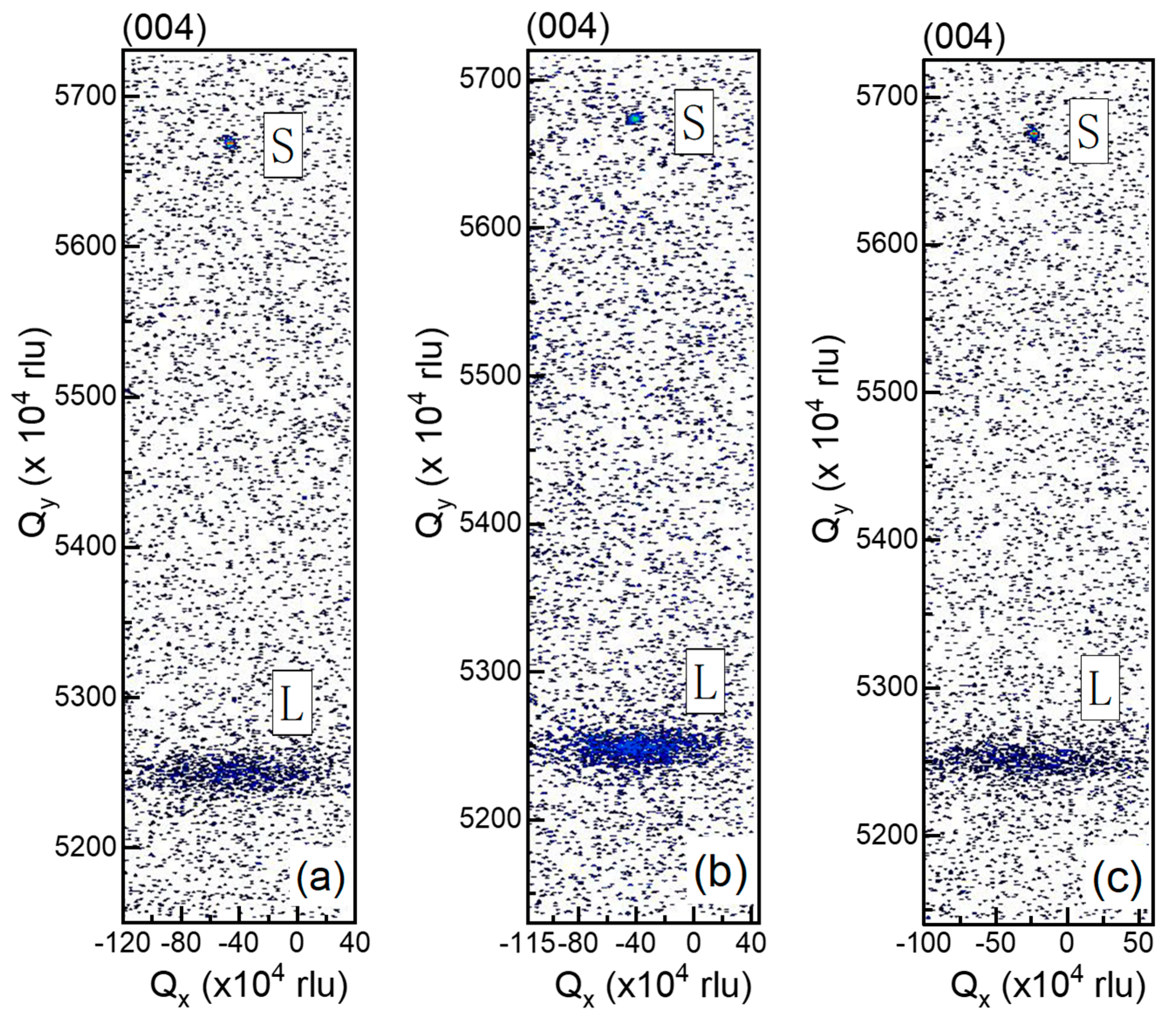
To further evaluate the crystal quality of the epitaxial layers, the XRD RSMs measurements were implemented in reflections of symmetric (004). Figure 6a–c show the XRD RSMs for Sample C, D, and E respectively with the intensities plotted on the logarithmic scale. The peak with relatively narrow and strong intensity corresponds to Si substrate which was denoted as S, and the wide peak corresponding to InP epi-layer was denoted as L in each RSM. According to the RSMs in Figure 6, it can be observed that the peak intensities of InP layer for sample D are stronger and narrower along the Qx direction than that for sample C and E, indicating the better crystal quality and lower density of defects with the nucleation layer grown at 350 °C. The conclusion is in accordance with the results presented by SEM, AFM images, RMS roughness, and XRD spectrum.
4. Conclusions
The influences of the InP nucleation layer on the two-step InP layers have been investigated at different growth temperature by GSMBE, and the results are compared with the findings in lots of similar studies. By growing nucleation layer at 350 °C, the smallest and fewest cavities at the InP/Si interface are observed by SEM images. Meanwhile, AFM images show that the surface islands become smaller and the pits become shallower at 350 °C, and the optimal RMS (10 × 10 μm2) roughness of 10.1 nm is obtained. Furthermore, the best results of the intensity and FWHM of (004) and (115) Bragg peaks and RSM measurement are achieved with the nucleation layer grown at 350 °C. All of these results indicate that the InP nucleation layer has the optimal growth temperature of 350 °C which strongly influences the growth process and crystal quality of InP film. Therefore, it is essential to determine the optimal growth temperature of nucleation layer to maximize the crystal quality of InP epi-layer grown on Si by the two-step growth method, thus realizing high-quality heterogeneous integration of InP and Si.
Author Contributions
Conceptualization, S.Y. (Shizheng Yang); Data curation, S.Y. (Shizheng Yang) and F.T.; Formal analysis, S.Y. (Shizheng Yang) and S.Y. (Silu Yan); Funding acquisition, H.L., L.A. and Y.Z.; Investigation, S.Y. (Shizheng Yang) and F.T.; Methodology, S.Y. (Shizheng Yang); Project administration, H.L. and L.A.; Resources, H.L., L.A. and Y.Z.; Software, S.Y. (Shizheng Yang); Supervision, H.L., L.A. and Y.Z.; Validation, S.Y. (Shizheng Yang) and L.A.; Visualization, S.Y. (Shizheng Yang) and S.Y. (Silu Yan); Writing—original draft, S.Y. (Shizheng Yang); Writing—review & editing, H.L., L.A. and S.Y. (Silu Yan).
Funding
This research was funded by National Natural Science Foundation of China, grant number 90304190002, the National Natural Science Foundation of China, grant number 61434006, and open project of State Key Laboratory of Infrared Physics, Shanghai Institute of Technical Physics, Chinese Academy of Sciences.
Acknowledgments
We would like to thank researcher Yan Sun from the Shanghai Institute of Technical Physics, Chinese Academy of Sciences for her assistance with the SEM measurements and analysis.
Conflicts of Interest
The authors declare no conflict of interest.
References
- Hiraki, T.; Aihara, T.; Hasebe, K.; Fujiia, T.; Takedaa, K.; Nishia, H.; Kakitsukaa, T.; Fukudaa, H.; Tsuchizawaa, T.; Matsuoa, S. Heterogeneous Integration of III-V Semiconductors on Si Photonics Platform. ECS Trans. 2018, 86, 11–16. [Google Scholar] [CrossRef]
- Lourdudoss, S.; Junesand, C.; Kataria, H.; Metaferia, W.; Omanakuttan, G.; Sun, Y.T.; Wang, Z.C.; Olsson, F. Trends in heteroepitaxy of III-Vs on silicon for photonic and photovoltaic applications. In Proceedings of the Smart Photonic and Optoelectronic Integrated Circuits XIX, San Francisco, CA, USA, 20 February 2017. [Google Scholar]
- Li, Q.; Lau, K.M. Epitaxial growth of highly mismatched III-V materials on (001) silicon for electronics and optoelectronics. Prog. Cryst. Growth Charact. Mater. 2017, 63, 105–120. [Google Scholar] [CrossRef] [Green Version]
- Kumar, A.; Lee, S.Y.; Yadav, S.; Tan, K.H.; Loke, W.K.; Dong, Y.; Lee, K.; Wicaksono, S.; Liang, G.; Yoon, S.F.; et al. Integration of InGaAs MOSFETs and GaAs/AlGaAs lasers on Si Substrate for advanced opto-electronic integrated circuits (OEICs). Opt. Express 2017, 25, 31853–31862. [Google Scholar] [CrossRef] [PubMed]
- Loke, W.K.; Lee, K.H.; Wang, Y.; Tan, C.S.; Fitzgerald, E.A.; Yoon, S.F. MOCVD growth of InGaP/GaAs heterojunction bipolar transistors on 200 mm Si wafers for heterogeneous integration with Si CMOS. Semicond. Sci. Technol. 2018, 33, 115011. [Google Scholar] [CrossRef]
- Green, D.S.; Dohrman, C.L.; Demmin, J.; Zheng, Y.; Chang, T.H. A Revolution on the Horizon from DARPA: Heterogeneous Integration for Revolutionary Microwave/Millimeter-Wave Circuits at DARPA: Progress and Future Directions. IEEE Microwav. Mag. 2017, 18, 44–59. [Google Scholar] [CrossRef]
- Mei, X.; Yoshida, W.; Lange, M.; Lee, J.; Zhou, J.; Liu, P.H.; Leong, K.; Zamora, A.; Padilla, J.; Sarkozy, S.; et al. First demonstration of amplification at 1 THz using 25-nm InP high electron mobility transistor process. IEEE Electron Device Lett. 2015, 36, 327–329. [Google Scholar] [CrossRef]
- Weimann, N.G.; Johansen, T.K.; Stoppel, D.; Matalla, M.; Brahem, M.; Nosaeva, K.; Boppel, S.; Volkmer, N.; Ostermay, I.; Krozer, V.; et al. Transferred-Substrate InP/GaAsSb heterojunction bipolar transistor technology with fmax~0.53 THz. IEEE Trans. Electron Devices 2018, 65, 3704–3710. [Google Scholar] [CrossRef] [Green Version]
- Urteaga, M.; Carter, A.; Griffith, Z.; Pierson, R.; Bergman, J.; Arias, A.; Rowell, P.; Hacker, J.; Brar, B.; Rodwell, M.J.W. THz bandwidth InP HBT technologies and heterogeneous integration with Si CMOS. In Proceedings of the 2016 IEEE Bipolar/BiCMOS Circuits and Technology Meeting (BCTM), New Brunswick, NJ, USA, 25–27 September 2016. [Google Scholar]
- Kazior, T.E. Beyond CMOS: Heterogeneous integration of III-V devices, RF MEMS and other dissimilar materials/devices with Si CMOS to create intelligent microsystems. Philos. Trans. R. Soc. A Math. Phys. Eng. Sci. 2014, 372, 20130105. [Google Scholar] [CrossRef] [Green Version]
- Nguyen, X.S.; Yadav, S.; Lee, K.H.; Kohen, D.; Kumar, A.; Made, R.I.; Lee, K.E.K.; Chua, S.J.; Gong, X.; Fitzgerald, E.A. MOCVD Growth of High Quality InGaAs HEMT Layers on Large Scale Si Wafers for Heterogeneous Integration with Si CMOS. IEEE Trans. Semicond. Manuf. 2017, 30, 456–461. [Google Scholar] [CrossRef]
- Megalini, L.; Šuran Brunelli, S.; Charles, W.; Taylor, A.; Isaac, B.; Bowers, J.; Klamkin, J. Strain-Compensated InGaAsP Superlattices for Defect Reduction of InP Grown on Exact-Oriented (001) Patterned Si Substrates by Metal Organic Chemical Vapor Deposition. Materials 2018, 11, 337. [Google Scholar] [CrossRef] [Green Version]
- Tournié, E.; Cerutti, L.; Rodriguez, J.; Liu, H.; Wu, J.; Chen, S. Metamorphic III–V semiconductor lasers grown on silicon. MRS Bull. 2016, 41, 218–223. [Google Scholar] [CrossRef]
- Kunert, B.; Mols, Y.; Baryshniskova, M.; Waldron, N.; Schulze, A.; Langer, R. How to control defect formation in monolithic III/V hetero-epitaxy on (100) Si? A critical review on current approaches. Semicond. Sci. Technol. 2018, 33, 93002. [Google Scholar] [CrossRef]
- Merckling, C.; Jiang, S.; Liu, Z.; Waldron, N.; Boccardi, G.; Rooyackers, R.; Wang, Z.; Tian, B.; Pantouvaki, M.; Collaert, N.; et al. Monolithic Integration of III-V Semiconductors by Selective Area Growth on Si (001) Substrate: Epitaxy Challenges & Applications. ECS Trans. 2015, 66, 107–116. [Google Scholar]
- Li, S.; Zhou, X.; Kong, X.; Li, M.; Mi, J.; Pan, J. Catalyst-free growth of InP nanowires on patterned Si (001) substrate by using GaAs buffer layer. J. Cryst. Growth 2016, 440, 81–85. [Google Scholar] [CrossRef]
- Shi, B.; Li, Q.; Lau, K.M. Self-organized InAs/InAlGaAs quantum dots as dislocation filters for InP films on (001) Si. J. Cryst. Growth 2017, 464, 28–32. [Google Scholar] [CrossRef]
- Li, Q.; Tang, C.W.; Lau, K.M. Growth of ultra-high mobility In0.52Al0.48As/InxGa1-xAs (x > = 53%) quantum wells on Si substrates using InP/GaAs buffers by metalorganic chemical vapor deposition. Appl. Phys. Express 2014, 7, 045502. [Google Scholar] [CrossRef]
- Huang, M.L.; Chang, S.W.; Chen, M.K.; Fan, C.H.; Lin, H.T.; Lin, C.H.; Chu, R.L.; Lee, K.Y.; Khaderbad, M.A.; Chen, Z.C.; et al. In0.53Ga0.47As MOSFETs with high channel mobility and gate stack quality fabricated on 300 mm Si substrate. In Proceedings of the 2015 Symposium on VLSI Technology (VLSI Technology), Kyoto, Japan, 27 August 2015. [Google Scholar]
- Li, J.; Miao, G.; Zhang, Z.; Zeng, Y. Experiments and analysis of the two-step growth of InGaAs on GaAs substrate. CrystEngComm 2015, 17, 5808–5813. [Google Scholar] [CrossRef]
- Okumura, S.; Suzuki, R.; Tsunoda, K.; Nishino, H.; Sugiyama, M. Suppression of Three-Dimensional Pit Formation of InAs on GaSb (001) by Two-Step MBE. In Proceedings of the 2019 Compound Semiconductor Week (CSW), Nara, Japan, 19–23 May 2019. [Google Scholar]
- Shin, K.W.; Kim, H.; Kim, J.; Yang, C.; Lee, S.; Yoon, E. The effects of low temperature buffer layer on the growth of pure Ge on Si (001). Thin Solid Films 2010, 518, 6496–6499. [Google Scholar] [CrossRef]
- Barrett, C.S.C.; Martin, T.P.; Bao, X.Y.; Kennon, E.L.; Gutierrez, L.; Martin, P.; Sanchez, E.; Jones, K.S. Effect of bulk growth temperature on antiphase domain boundary annihilation rate in MOCVD-grown GaAs on Si(001). J. Cryst. Growth 2016, 450, 39–44. [Google Scholar] [CrossRef]
- Li, J.; Guo, Z.; Zhao, L.; Jia, Z.; Zhang, M.; Zhao, L. Effect of thicknesses of InP epilayers on InP/GaAs heterostructure. Surf. Interface Anal. 2018, 50, 27–31. [Google Scholar] [CrossRef]
- Cho, Y.; Lee, I.; Kim, S.; Jun, D.; Choi, I.; Kwon, H.; Shin, C.; Park, K.; Park, W.; Kim, D.; et al. Two-Step Growth of Epitaxial InP Layers by Metal Organic Chemical Vapor Deposition. J. Nanosci. Nanotechnol. 2016, 16, 5168–5172. [Google Scholar] [CrossRef] [PubMed]
- Lee, S.; Cho, Y.J.; Park, J.; Shin, K.W.; Hwang, E.; Lee, S.; Lee, M.; Cho, S.; Su Shin, D.; Park, J.; et al. Effects of growth temperature on surface morphology of InP grown on patterned Si(001) substrates. J. Cryst. Growth 2015, 416, 113–117. [Google Scholar] [CrossRef]
- Kwoen, J.; Jang, B.; Lee, J.; Kageyama, T.; Watanabe, K.; Arakawa, Y. All MBE grown InAs/GaAs quantum dot lasers on on-axis Si (001). Opt. Express 2018, 26, 11568. [Google Scholar] [CrossRef] [PubMed]
- Liu, A.Y.; Peters, J.; Huang, X.; Jung, D.; Norman, J.; Lee, M.L.; Gossard, A.C.; Bowers, J.E. Electrically pumped continuous-wave 1.3 μm quantum-dot lasers epitaxially grown on on-axis (001) GaP/Si. Opt. Lett. 2017, 42, 338–341. [Google Scholar] [CrossRef]
- Jung, D.; Callahan, P.G.; Shin, B.; Mukherjee, K.; Gossard, A.C.; Bowers, J.E. Low threading dislocation density GaAs growth on on-axis GaP/Si (001). J. Appl. Phys. 2017, 122, 225703. [Google Scholar] [CrossRef] [Green Version]
- Crumbaker, T.E.; Lee, H.Y.; Hafich, M.J.; Robinson, G.Y. Growth of InP on Si substrates by molecular beam epitaxy. Appl. Phys. Lett. 1989, 54, 140–142. [Google Scholar] [CrossRef]
- Ayers, J.E. The measurement of threading dislocation densities in semiconductor crystals by X-ray diffraction. J. Cryst. Growth 1994, 135, 71–77. [Google Scholar] [CrossRef]
Figure 1.
Schematic of InP epitaxial structures on Si (001) substrate.
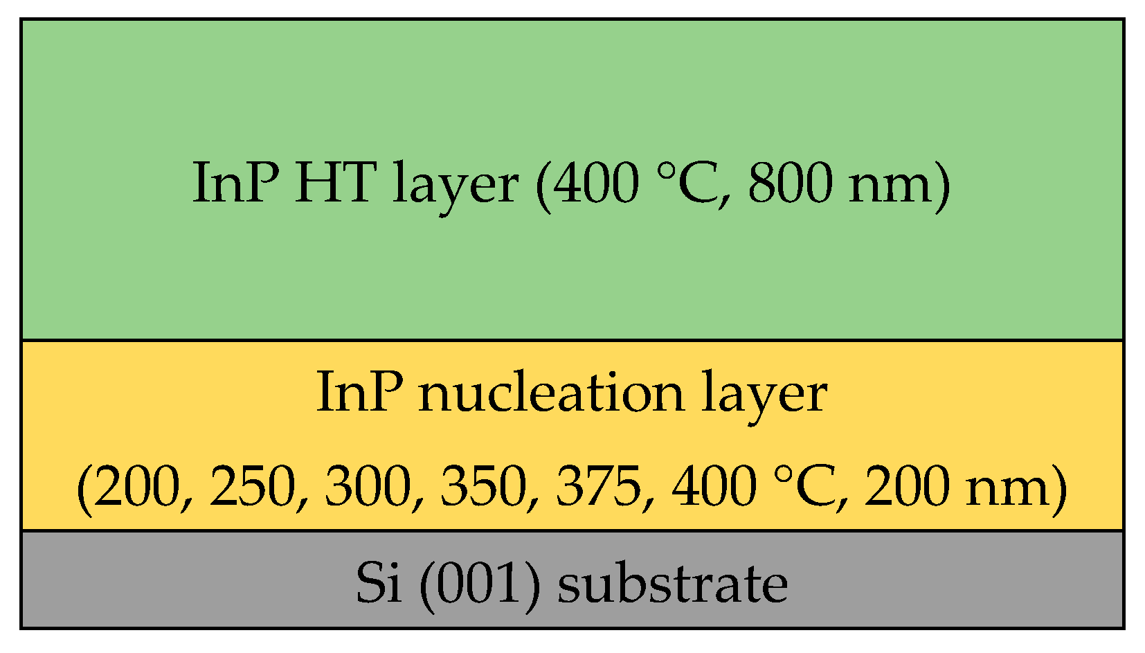
Figure 2.
Cross-sectional SEM images of the 1 μm InP epi-layer with nucleation layer grown at different temperature: (a1,a2) 200 °C, (b1,b2) 250 °C, (c1,c2) 300 °C, (d1,d2) 350 °C, (e1,e2) 375 °C, and (f1,f2) 400 °C. (a1–f1) and (a2–f2) are the SEM images magnified 50,000 and 100,000 times, respectively. Some streaks at the cleavage plane are artifacts during the SEM sample preparation. Red circles indicate the noticeable cavities.

Figure 3.
AFM images of InP films with nucleation layer grown at different temperature: (a) 200 °C, (b) 250 °C, (c) 300 °C, (d) 350 °C, (e) 375 °C, and (f) 400 °C in a 10 × 10 μm2 scanning area.
Figure 3.
AFM images of InP films with nucleation layer grown at different temperature: (a) 200 °C, (b) 250 °C, (c) 300 °C, (d) 350 °C, (e) 375 °C, and (f) 400 °C in a 10 × 10 μm2 scanning area.
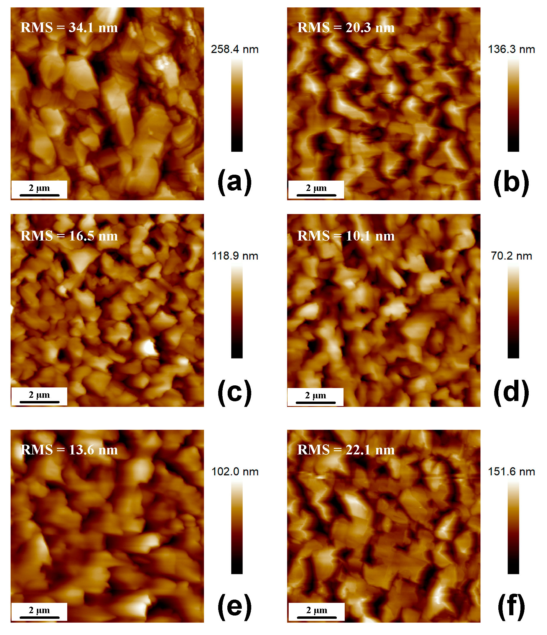
Figure 4.
Plot of the RMS roughness of InP films versus different growth temperature of InP nucleation layer.
Figure 4.
Plot of the RMS roughness of InP films versus different growth temperature of InP nucleation layer.
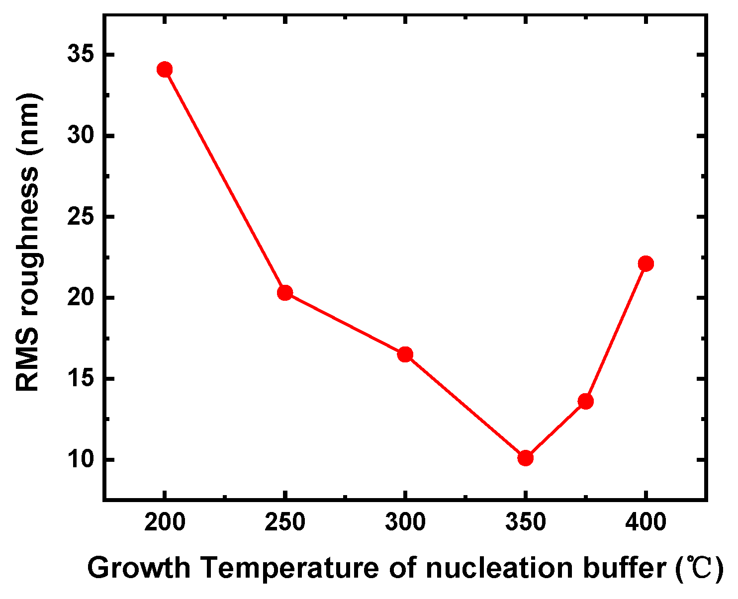
Figure 5.
(004) and (115) Ω-2θ HR-XRD scan curves for all samples.

Figure 6.
Symmetric (004) XRD RSMs of (a) sample C, (b) sample D, and (c) sample E.

Table 1.
Intensity and FWHM of (004) and (115) Bragg peaks for all samples.
| Sample | Intensity of 004 (a.u) | FWHM of 004 (arcsec) | Intensity of 115 (a.u) | FWHM of 115 (arcsec) |
|---|---|---|---|---|
| A | 44 | 1657.6 | 30 | 1806.82 |
| B | 128 | 1627.43 | 61 | 1619.11 |
| C | 355 | 1512.8 | 160 | 1464.3 |
| D | 495 | 1507.08 | 247 | 1236.85 |
| E | 283 | 1608.47 | 123 | 1427.2 |
| F | 208 | 1679.73 | 88 | 1639.5 |
© 2019 by the authors. Licensee MDPI, Basel, Switzerland. This article is an open access article distributed under the terms and conditions of the Creative Commons Attribution (CC BY) license (http://creativecommons.org/licenses/by/4.0/).
Share and Cite
MDPI and ACS Style
Yang, S.; Lv, H.; Ai, L.; Tian, F.; Yan, S.; Zhang, Y. Influence of Growth Temperature of the Nucleation Layer on the Growth of InP on Si (001). Coatings 2019, 9, 823. https://doi.org/10.3390/coatings9120823
AMA Style
Yang S, Lv H, Ai L, Tian F, Yan S, Zhang Y. Influence of Growth Temperature of the Nucleation Layer on the Growth of InP on Si (001). Coatings. 2019; 9(12):823. https://doi.org/10.3390/coatings9120823
Chicago/Turabian StyleYang, Shizheng, Hongliang Lv, Likun Ai, Fangkun Tian, Silu Yan, and Yuming Zhang. 2019. "Influence of Growth Temperature of the Nucleation Layer on the Growth of InP on Si (001)" Coatings 9, no. 12: 823. https://doi.org/10.3390/coatings9120823
Note that from the first issue of 2016, this journal uses article numbers instead of page numbers. See further details here.