Article

Analysis of Sn Concentration Effect on Morphological, Optical, Electrical and Photonic Properties of Spray-Coated Sn-Doped CdO Thin Films

1
Millimeter-wave Innovation Technology (MINT) Research Center, Dongguk University-Seoul, Seoul 04620, Korea
2
Periyar Maniammai University, Thanjavur, Tamil Nadu-613403, India
3
Division of Electronics and Electrical Engineering, Dongguk University-Seoul, Seoul 04620, Korea
*
Author to whom correspondence should be addressed.
Coatings 2018, 8(5), 167; https://doi.org/10.3390/coatings8050167
Submission received: 29 March 2018 / Revised: 21 April 2018 / Accepted: 24 April 2018 / Published: 27 April 2018

Abstract

:
Tin-doped cadmium oxide (Sn:CdO) transparent thin films with different Sn concentrations were deposited on glass and p-silicon substrates by the chemical spray method at 250 °C. Different concentrations of stannic chloride were used to prepare Sn:CdO thin films. The prepared doped and un-doped CdO films were subjected to X-ray diffraction (XRD), scanning electron microscopy and atomic force microscopy, optical absorption, and electrical analyses to characterize their structural, morphological, optical, and electrical properties, respectively. XRD analysis demonstrated the growth of polycrystalline and cubic CdO with preferential orientation along the (111) plane. Sn-doping shifted the XRD peaks slightly towards a higher Bragg angle and increased the band gap of CdO thin films. Variation in doping concentration also affected the morphology of the films. Optimum Sn-doping increased the electrical conductivity of CdO thin films. Furthermore, to the best of our knowledge, the photoresponse analyses of the fabricated un-doped and doped n-CdO/p-Si heterostructures were performed for the first time in this study.

1. Introduction

The transparent conducting oxide (TCO) thin films, such as tin oxide, zinc oxide, indium tin oxide, and cadmium oxide (CdO), have attracted considerable attention due to their potential applications in various fields [1,2,3]. Among the various TCO materials, CdO is particularly interesting because of its low resistivity, high carrier concentration, and high optical transmittance in the visible region [4]. CdO is extensively used for optoelectronic applications such as transparent electrodes, photovoltaics, sensors, optical communications, and flat panel displays [5,6]. It is an n-type semiconductor with a rock-salt crystal structure (FCC) possessing a direct band gap of 2.3–2.5 eV [7]. Although it has high electrical conductivity, its applications are limited due to its low band gap energy. However, doping can be used to widen its band gap without compromising its electrical properties. Moreover, doping is also required to improve the quality and performance of semiconductor devices and for novel applications [8,9]. CdO can be doped with aluminum [10,11], titanium [12], indium [13], gallium [14], manganese [15], magnesium [16], zinc [17], tin (Sn), etc. to make it suitable for various applications. However, Sn is a highly suitable dopant for CdO because the Sn4+ ion has a smaller ionic radius (0.7 Å) than Cd2+ ion (0.95 Å). Hence, through doping, Sn can improve the crystalline structure and electrical properties of CdO by increasing electron concentration [18].
For the growth of CdO and Sn-doped CdO (Sn:CdO), a variety of techniques such as pulsed laser deposition [13,19], metal-organic chemical vapor deposition (MOCVD) [20], successive ionic layer adsorption and reaction (SILAR) [21], chemical bath deposition [22], RF magnetron sputtering [23], sol-gel processing [18], thermal evaporation [24], and spray pyrolysis [25] are used. Amongst all, the spray pyrolysis method is quite enticing due to its simplicity, ease of composition control, and better doping possibilities. In this study, we aim to investigate the effects of Sn-concentration on morphological, structural, optical, and electrical properties of Sn:CdO. Sn-doping-induced better optical and electrical properties improve the overall performance of TCO-based solar cells and other optical devices. However, Sn:CdO growth by a variety of methods is already explained by several research groups [18,22,24]; however, information on spray-coated Sn:CdO growth is limited. Moreover, to the best of our knowledge, the n-Sn:CdO/p-Si heterostructure and photoresponse analyses are propounded for the first time. Generally, Sn:CdO is used for window layers in photovoltaic applications because of its high transparency in the visible region. However, as a high band gap n-type semiconductor, Sn:CdO-based heterojunction solar cells can also be fabricated on p-Si substrates. In addition, the heterojunction formed between Sn:CdO and p-Si can minimize recombination loss due to a combination of high band gap window material and small band gap absorber material. Hence, besides probing into the material properties, this study is focused on testing the photoresponse mechanism of n-Sn:CdO/p-Si heterojunction diodes.

2. Materials and Methods

CdO thin films were deposited on p-Si and glass substrates by dissolving 0.05 M cadmium acetate in 25 mL deionized (DI) water. For Sn-doping, various concentrations (0.1, 0.2, and 0.3 mM) of stannic chloride (SnCl4) were dissolved in 25 mL DI water. To prepare the spray solution, cadmium acetate and SnCl4 (25 mL each) were mixed and stirred for 20 minutes at room temperature. Before the precursor solution was sprayed, the substrates were cleaned with soap solution and acetone, which were then dried. A desired volume of the precursor solution was sprayed from the spray nozzle onto the preheated substrates, which were kept at 250 °C. In order to maintain the temperature at 250 °C during the spraying of the solution, the hot plate of the electric oven was controlled by a chromo-alumino temperature controller. The spray nozzle prepared with double-walled design was placed at a distance of approximately 35 cm from the substrate. The solution was sprayed at an angle of 45° for 5 s. There was a time gap of 15 s between successive sprays to avoid excessive cooling and to maintain a constant temperature on the substrate surface. Compressed carrier gas at a pressure of 2 kg cm−2 was released from the air compressor through an air filter and regulator to produce a fine mist for uniform spray. The various concentrations of precursor solution used for Sn-doping are shown in Table 1. After deposition, the structural, morphological, optical, and electrical properties of the films were analyzed. The film structure was characterized using an X-ray diffractometer (XRD, PANalytical, Almelo, The Netherlands) with Cukα radiation (λ = 1.54056 Å). Morphological analysis of the films was performed using a scanning electron microscope (SEM, ESEMQUANTA200, FEI, Hillsboro, OR, USA). Film thickness was measured via a profilometer (SJ-301, Mitutoyo, Kanagawa, Japan). The optical transmittance of the films was recorded using a UV-VIS spectrophotometer (HR2000, Oceans Optics, Largo, FL, USA).
Spectrofluorometer was used to obtain photoluminescence spectra of the films. Electrical measurements were conducted using a Hall Effect measurement system (Ecopia HMS-3000, Bridge Technologies, Phoenix, AZ, USA) in van der Pauw four probe configuration at room temperature with 0.3 T magnetic field. The diode properties of the fabricated n-Sn:CdO/p-Si heterostructure were measured using Keithley 4200-SCS electrical parameter analyzer (Solon‎, OH, USA) at room temperature.

3. Results and Discussion

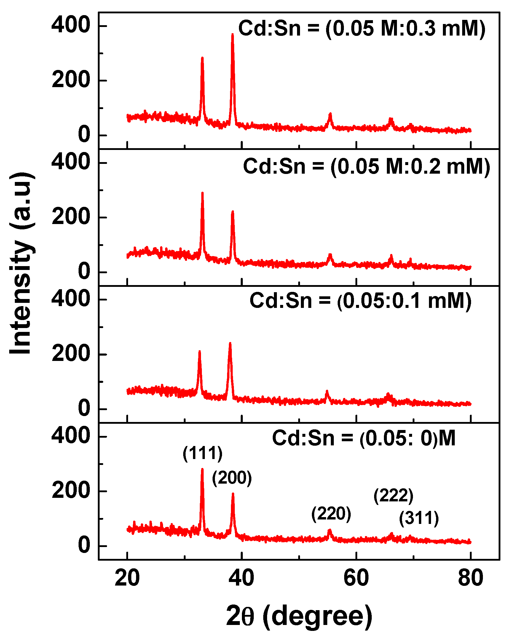
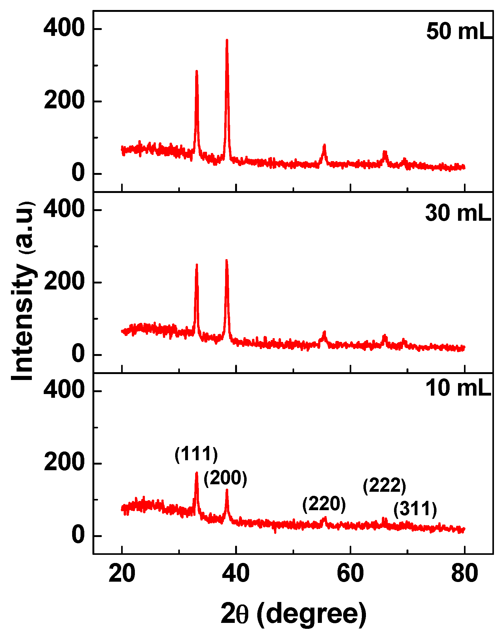
3.1. Structural Analysis

Figure 1 shows the XRD pattern of un-doped and Sn:CdO thin films deposited using 50 mL SnCl4 (0.1, 0.2, and 0.3 mM) solutions. The XRD spectrum was recorded in the 2θ range from 20° to 80°. The XRD peaks are in agreement with JCPDS card [005-0640], indicating the polycrystalline and face-centered cubic structure of CdO films. The peaks were indexed to the (111), (200), (220), (222), and (311) planes with respect to standard XRD lines. In addition, compared to the standard JCPDS line, all the peaks were broadened in their shapes. All the Sn:CdO films showed a preferential growth along the (111) and (200) planes with increased intensity following an increase in Sn concentration. This increase in peak intensity indicated that there might be an improvement in the crystalline structure of the film due to an increase in doping concentration. The (111) peak position was slightly shifted towards the (200) peak when doping concentration was increased, which was attributed to the shrinkage of the CdO crystal lattice due to the substitution of the smaller radius Sn4+ ion with Cd2+. The most favored orientation of Sn:CdO was changed to the (200) plane compared to un-doped CdO.
Compared to un-doped CdO films’ orientation (111), all of the doped CdO films showed a (200) orientation plane as most favored orientation except for the Sn concentration of 0.2 mM. This arbitrary change in crystallite orientation is also often possible in Sn-doped CdO due to the changes associated with oxygen vacancies and Sn substitutes by Sn-doping concentration variation. Similarly, a small change in growth temperature can also change the crystallite orientation. A same trend of XRD peak intensity reversion depending on substrate temperature and an increase in Sn-doping concentration has also been reported in the literature [20,26,27,28]. Zhao et al. [20] and Gupta et al. [26] showed temperature-dependent crystallite orientation change in Sn-doped CdO thin films prepared by MOCVD and pulsed laser deposition (PLD), respectively. Zheng et al. [27] showed crystallite orientation change in PLD-prepared Sn-doped CdO thin films due to the variation in Sn-doping concentration. Ghosh et al. [28] reported growth condition-dependent change in crystallite orientation of Sn-doped CdO synthesized by solution route.
Figure 2 shows the XRD pattern of the films prepared using different volumes of cadmium acetate (0.05 M) and SnCl4 (0.3 mM). The peak intensity was increased with an increase in solution volume. In comparison between the peak intensities of the films coated using 10 mL and 50 mL of the solutions, the favored orientation was changed from the (111) plane to the (200) plane. The reported change in the preferential plane from (111) to (200) is attributed to changes in the internal stress due to Sn-doping, which can alter the energetic balance between different crystal plane orientations and lead to a preferred texture. Furthermore, the peak shift and broadening of diffraction lines are caused by changes in the microstrain of the films [29]. Therefore, the change in strain with volume and concentration should be further investigated.

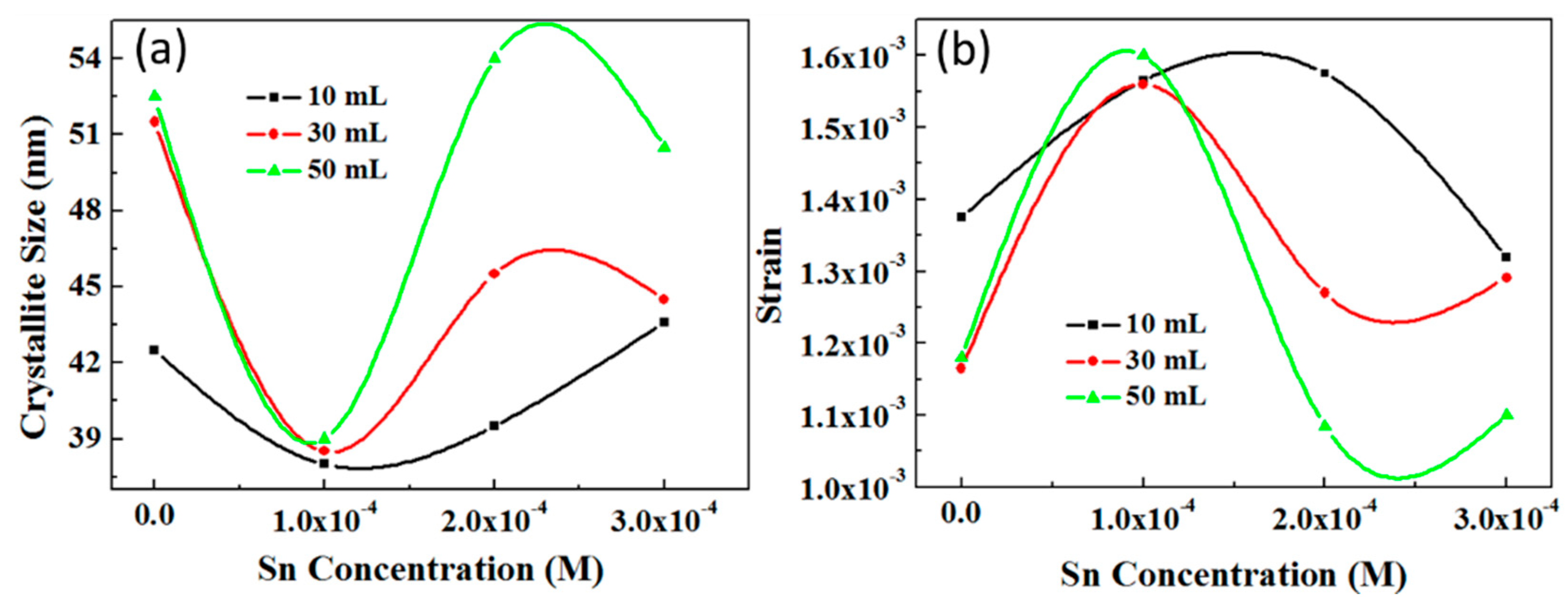
3.2. Crystallite Size and Strain Analysis

The crystallite size of the films was estimated using the X-ray line broadening technique employing the Debye Scherrer formula shown in Equation (1) [30]:
D   =   K λ β cos   θ
where β is the full width at half maximum (FWHM) of the (111) peak in radians, λ is the wavelength of the incident X-ray (1.541 Å), θ is the angle at which the maximum peak occurs, and K is the shape factor, which usually takes a value of around 0.89. Figure 3 shows the change in crystallite size and strain with the change in the Sn concentration and volume of the precursor solution. Crystallite size was found to vary in the range of 38–54 nm for 0.1–0.3 mM of Sn and 10–50 mL of the precursor solution.
As shown in Figure 3a, crystallite size was decreased initially, and it was increased with a further increase in Sn concentration in a particular volume of solution. An Sn concentration of 0.1 mM resulted in only slight changes in crystallite size, as demonstrated by XRD results. An increase in solution volume was found to increase the size of the crystallites, which is attributed to the increase in the number of species involved in the formation of CdO films. The decrease in crystallite size with increased doping concentration is because of the change in strain. Strain (ε) variation in the films was calculated using Equation (2) [31], and its dependence on the Sn concentration and volume of the solution are shown in Figure 3b:
ε = β cos θ 4
The trend was similar to the change in crystallite size but in the opposite direction. An increase in crystallite size decreased the microstrain, which indicated peak movement without any change in the peak shape. The observed changes in strain were because of point defects and the change in crystallite size. Based on Figure 3, it is inferred that higher volume (0.2 mM) leads to the maximum crystallite size and minimum strain.
For Sn-doping of concentration 0.1 mM, the favored crystallite orientation was changed from (111) plane to (200) plane. Slight increase of Sn concentration (0.2 mM) combined with a thermal effect produced an enhanced crystallite size causing increased XRD peak intensity. Further increase in Sn doping concentration to 0.3 mM reverted the intensity of the peaks. It is because of the re-orientation of the crystallites at this concentration. Furthermore, a slight increase in substrate temperature may also increase the crystallite size [32]. Small amount of Sn-doping concentration allows coalescence of crystallites and increases the size. The incorporation of Sn atoms into the CdO lattice can produce Sn substitutes, oxygen vacancies, and associated stress variation. These changes can slightly increase the lattice parameter causing crystallite size improvement. The crystallite re-orientation affects the shape and phase of the peaks, which could alter the crystallite size. At higher doping concentrations, the effect of Sn4+ ions is more pronounced. The substitution of Sn4+ ions of smaller radius (1.41 Å) with Cd2+ ions of larger radius (1.48 Å) shrinks the CdO crystal lattice, which reduces the crystallite size [27].

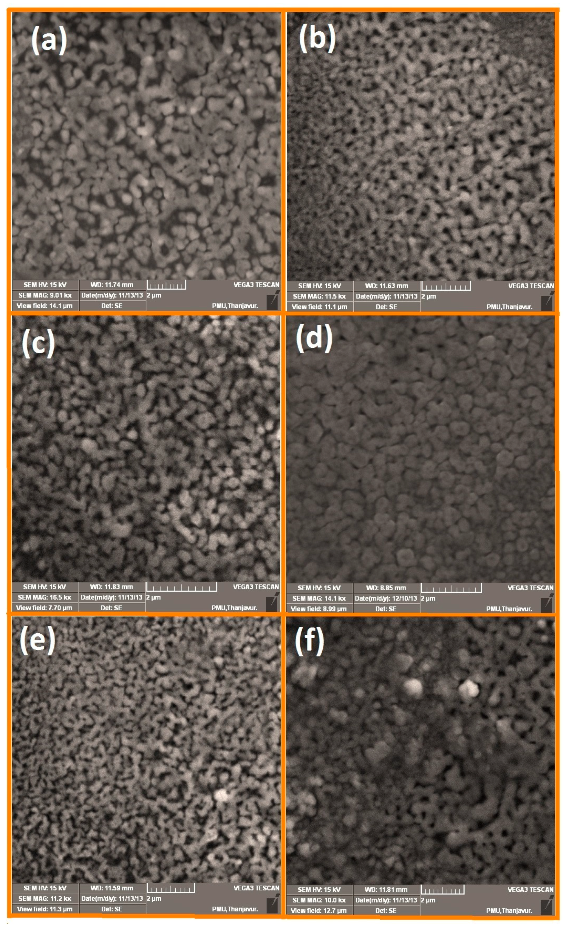
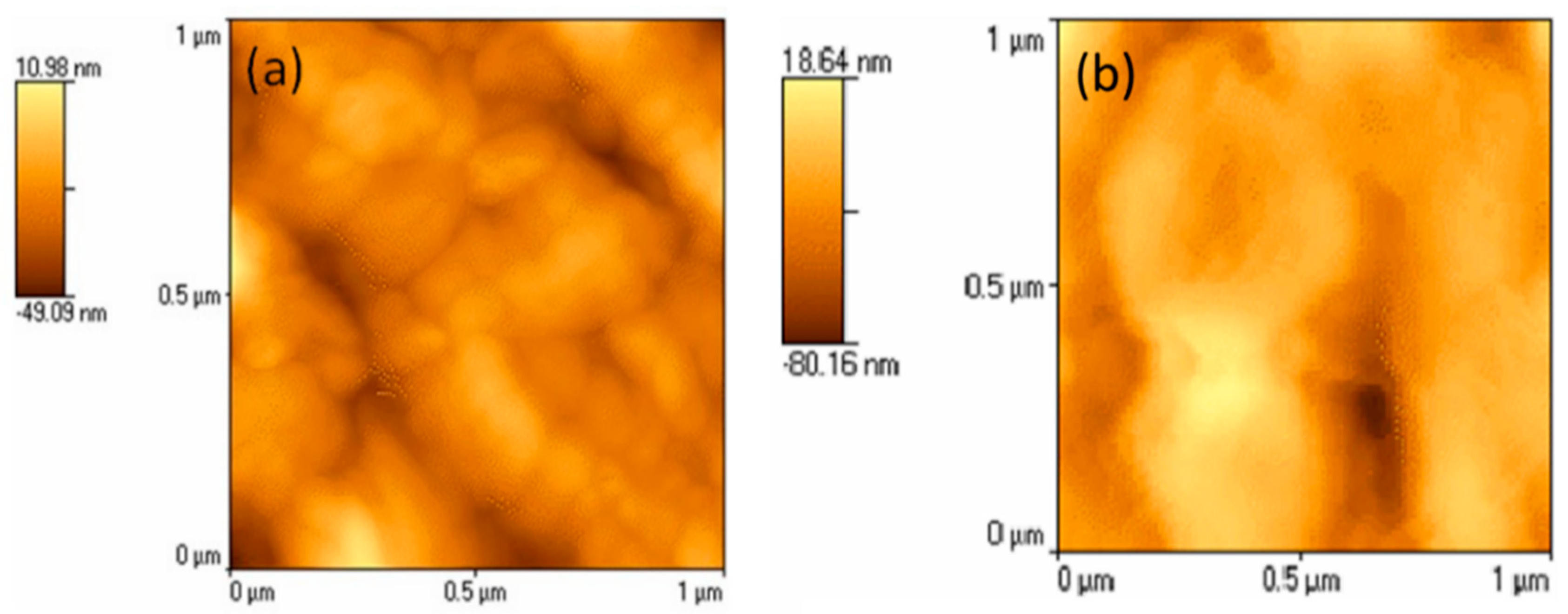
3.3. Morphological Evaluation

SEM Figure 4 shows the variation in the surface morphology of Sn:CdO thin films prepared using two different volumes (10 and 50 mL) of various Sn concentrations (0.1, 0.2, and 0.3 mM). The deposits were uniform spherical grains packed closely without cracks, and they were well adherent with the substrate. The films deposited with 50 mL solution were less porous, but they were a dense cluster of particles. The microphotographs revealed that the surface roughness of the films was decreased with an increase in Sn-doping. This finding indicated that the grain size and surface roughness of CdO films could be controlled by Sn-doping. Grain size was increased with increasing Sn concentration. The increase in grain size suggests improved crystallinity with decreased grain boundary. Hence, scattering due to grain boundary is reduced, which results in an increase in conductivity [33].
The topographical image of un-doped CdO and Sn:CdO (10 mL of 0.3 mM Sn) taken by atomic force microscopy (AFM) is shown in Figure 5. The CdO film (Figure 5a) consisted of closely packed uniform spherical agglomerated grains without cracks. This indicated that the film was well adherent with the substrate. Moreover, grain-like mounts with no well-defined boundaries were observed. The average roughness of the CdO film was 6.43 nm. The Sn:CdO film (Figure 5b) showed homogeneous, vertically grown grains packed closely with little voids. The average roughness of the Sn:CdO film was 16.38 nm.

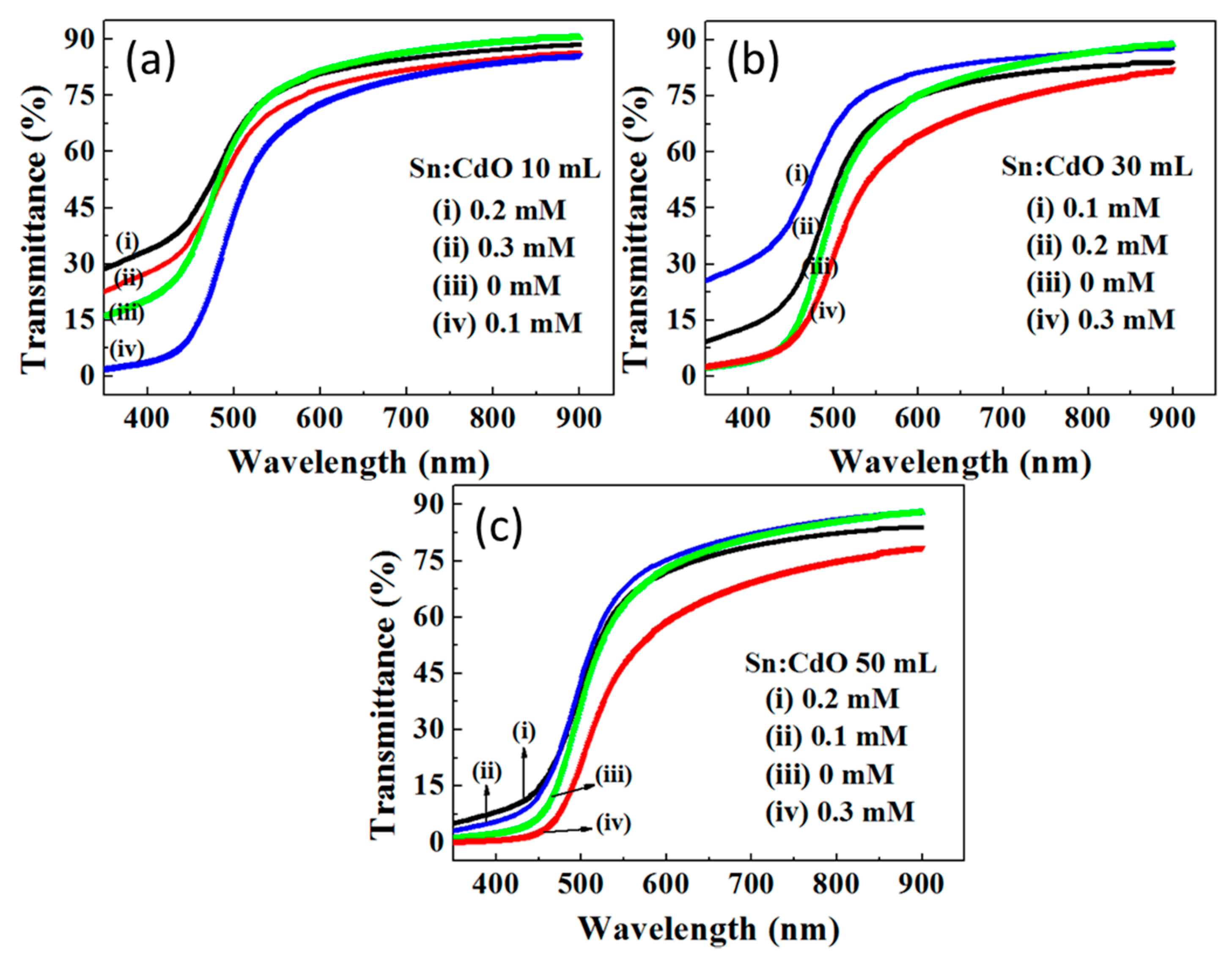
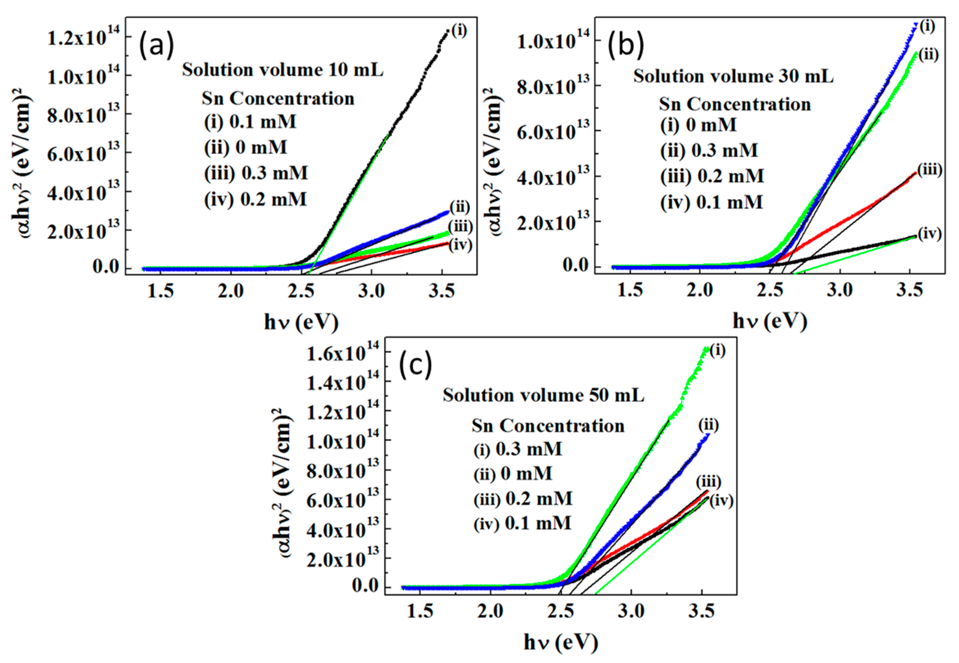
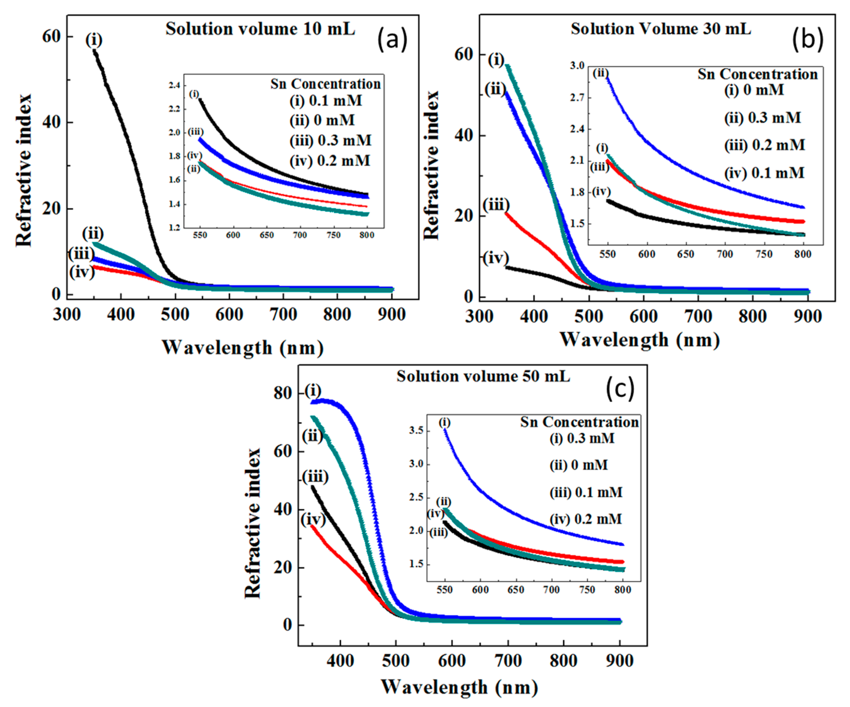
3.4. Optical Characterization

Sn:CdO films were transparent and light yellow in color. The color of the films was found to increase with an increase in precursor solution volume, and it became lighter when Sn concentration was increased. In order to determine the optical properties of Sn-doped and un-doped CdO thin films, the effect of Sn concentration on transmittance, refractive index, and optical band gap was evaluated. The optical transmission spectra of the films were recorded in the wavelength region of 350–900 nm. Figure 6a–c shows the optical transmittance of Sn:CdO films prepared under optimized conditions. There was a smooth increase in transmittance from 500–900 nm for all films with a slight variation depending on the concentration and volume. All the transmittance values corresponding to the Sn volume and concentration are summarized in Table 2. The maximum transmittance was around 88% at 900 nm for 0.2 mM of Sn. The high transmittance values of Sn: CdO thin films indicated that the films could be used as a window layer in solar cells. The high transparency in the visible and near infrared regions is in good agreement with previously reported results for CdO thin films [34]. In general, the transmittance decreases with increased solution volume and Sn concentration. However, un-doped CdO showed maximum transparency at higher wavelengths irrespective of doping concentration and solution volume. The decrease in transmittance at higher doping levels is credited to an increase in photon scattering due to crystal defects caused by doping or an increase in the metal-to-oxygen ratio in the film. Indeed, the metal-to-oxygen ratio may affect the transmission if the sample is metal-rich; it can result in low transmission [35].
The optical absorption edge was found to vary depending on the solution concentration and volume. Interestingly, the absorption edge of Sn:CdO thin films was blue-shifted (400–500 nm). Therefore, as doping concentration was increased, the (Cd + Sn)/O ratio was also increased. XRD and SEM analyses demonstrated an increase in grain size and surface roughness as the concentration was increased, which led to a reduction in optical transmission.
In order to investigate the effect of doping concentration on optical band gap of the CdO thin films, the optical band gap was determined by the optical absorption method. As the CdO is a direct band-gap semiconductor, we used the following relation to find an optical band gap (Equation (3)) [36]:
( h ν ) 1 / n = A ( h ν E g )
where A is a constant, Eg is the optical band gap of the material and n is a constant that determines the type of optical transitions and for indirect allowed transition n = 2; and indirect forbidden transition n = 3; for direct allowed transition n = 1/2; for direct forbidden transition, and n = 3/2. The absorption coefficient (α) was calculated using the Equation (4):
α = ln ( 1 / T ) d
where T is transmittance and d is film thickness.
We have plotted (αhυ)2 vs hυ curves for different films taking n as ½ and they are shown in Figure 7. The linear nature of the curves indicates the direct band to band transition of the films. The band gap values of the films were calculated by extrapolating the linear portion of the graph to the x-axis. A small increase of band gap approximately 0.2 eV was observed after the doping of tin preferable at a low concentration (0.2 mM). The change of band gap values corresponding to the solution volume and Sn-doping concentration is summarized in Table 3.
The blue shift in the Sn:CdO absorption spectra is because of the Burstein–Moss effect. The band gap value of CdO:Sn films was found to vary from 2.48–2.69 eV with increasing Sn concentration, which is in agreement with earlier findings [27]. When doping concentration was increased, the Fermi level was shifted to higher energy states due to the electron populated states in the conduction band, which could cause band broadening [37]. This band gap widening is important for TCO applications such as solar cells.
Refractive index is also one of the key parameters that can be used to understand the optical properties of materials. The refractive index of various films was determined using Equation (5) [38]:
n   =   1 + R 1 R + 4 R ( 1 R ) 2 k 2
where k = αλ/4π is the extinction coefficient. The calculated refractive index values of doped and un-doped CdO thin films with different Sn concentrations and precursor volumes are shown in Figure 8. To calculate the refractive index of the films, substrate effects were removed. The refractive index values of un-doped and Sn:CdO films showed a slight and smooth degradation above 700 nm.
However, the change was not distinct due to the inclusion of Sn. A higher Sn concentration was associated with the maximum refractive index with a higher volume of the precursor solution. The wavelength-dependent refractive index variation of the films prepared using 30 mL solution with different Sn concentrations is shown in the Table 4.
Room-temperature photoluminescence spectra of CdO and Sn:CdO films were obtained using the Cary Eclipse EL08083851 Spectrofluorometer (Agilent, Santa Clara, CA, USA) in emission scanning mode in the wavelength range of 415–750 nm. Figure 9 shows the emission peaks obtained for un-doped and Sn:CdO films; there were five emission peaks centered at 458.93 nm, 484.92 nm, 527.91 nm, 539.85 nm, and 711.97 nm. Photoluminescence results indicated that pure CdO exhibited low luminance compared to Sn:CdO. The intensity of emission peaks was found to increase with an increase in doping concentration. This increase in peak intensity demonstrated a decrease in defect sites following an increase in doping concentration.

3.5. Electrical Properties

The electrical resistivity of the films was calculated using the four-point probe method and employing the Equation (6) [39]:
ρ = π t ln 2 R s
where t is the thickness and Rs is the sheet resistance. Figure 10 shows the temperature-dependent variation in resistivity as a function of Sn concentration in CdO thin films. All films demonstrated a linear increase in resistivity with temperature; however, films with a Sn concentration of 0.2 mM showed a slightly different trend. The resistivity was decreased for films with an Sn concentration of 0.1 mM and 0.3 mM. On the contrary, it was increased for films with an Sn concentration of 0.2 mM. In the case of 0.2 mM of Sn, the resistivity was higher at low temperatures but was decreased at a higher temperature, which is due to temperature-dependent changes in the crystalline phase. XRD results indicated that the favored orientation was concentration-dependent. The reduction in electrical resistivity at higher concentrations may result from a reduction in voids and improved carrier concentration. Furthermore, electrical conductivity and mobility are more sensitive to grain interface than crystal defects. Hence, enhanced conductivity at a higher temperature and higher concentration is attributed to an improvement in the grain interface. Typically, non-stoichiometric un-doped CdO thin films exhibit low resistivity due to the native defects of oxygen vacancies and cadmium interstitials [25].
Hall measurements were performed at room temperature in order to examine the electrical properties of the films. It confirmed the n-type conductivity of the prepared films. Figure 11a,b shows the variation of resistivity, conductivity, carrier concentration and mobility of the films for different Sn-doping concentrations of volume 30 mL solution. The electrical resistivity of the deposited Sn:CdO films was increased as Sn concentration increased. However, the Sn concentration of 0.2 mM showed slightly lesser resistivity compared to the other concentration. The carrier concentration of Sn:CdO films was found to increase with the increase of doping concentration. Mobility of the films was decreased for the increase of Sn concentration. The increase of carrier concentration might have aroused by the generation of extra electrons due to Sn-doping because the substitution of each Sn4+ ions with Cd2+ ions can liberate two free electrons in the conduction band causing carrier addition. The Sn concentration of 0.2 mM had produced reasonably good electrical property compared to other concentrations.

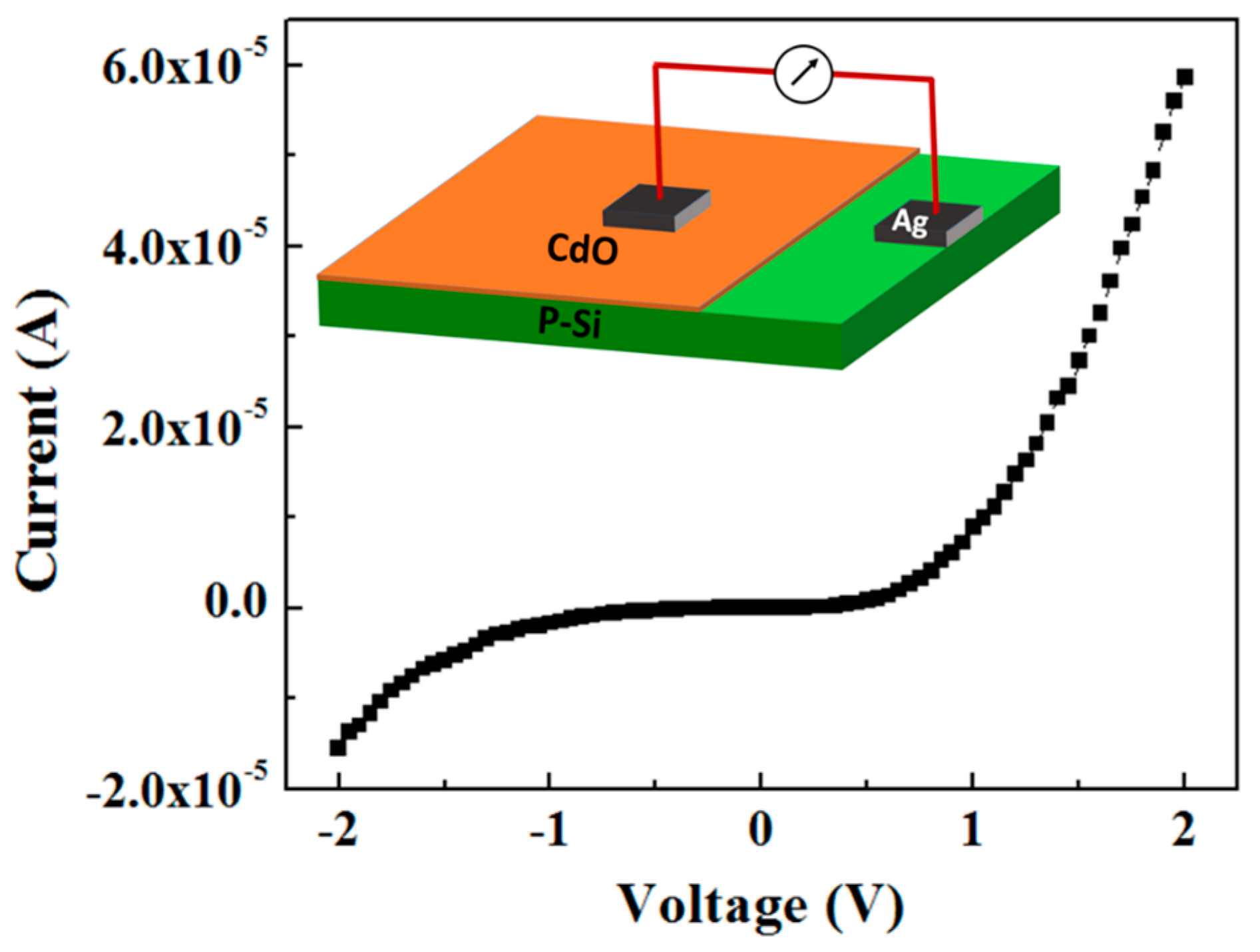
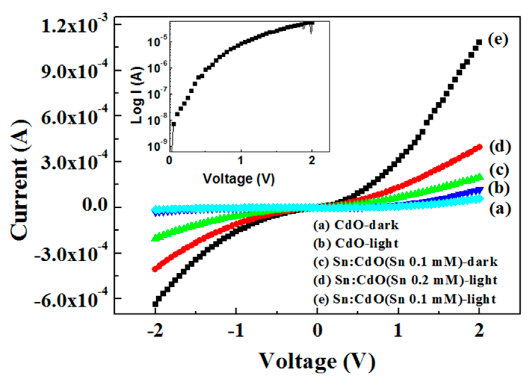
3.6. Photodiode Analysis

The measured current-voltage (I-V) curve of the Ag/n-CdO/p-Si/Ag device is shown in Figure 12 under dark conditions. The inset shows schematic view of the fabricated device. The dark current was increased with an increase in the applied voltage, where the device had a rectification ratio (IF/IR) of 3.6 at 2 V. This result confirmed the formation of a heterojunction diode between n-CdO and p-Si. Current passing through the heterojunction device is expressed by Equation (7) [40]:
I = I O ( exp q V n k T 1 )
where Io is the reverse saturation current, V is the applied voltage, q is the electronic charge, n is the ideality factor, k is the Boltzmann constant, and T is the temperature. The ideality factor (n) was obtained from the slope of the semi-log dark I-V plot (inset, Figure 13). The n was 2.8 at around 1 V, and the reverse saturation current was 5.58 × 10⁻⁶ A. The n was greater than unity, which is associated with the effects of the interface states, native oxide layer, and series resistance. This further confirms the dominance of recombination current in the transport mechanism of the device [41].
In order to evaluate the photoconduction properties of the fabricated Ag/n-CdO/p-Si/Ag photodiode, I-V measurements were performed under optical illumination. Figure 13 shows the I-V characteristics of the device with different Sn concentrations under optical illumination. There was a strong variation in both the forward and reverse currents under illumination. In comparison to un-doped CdO, Sn:CdO demonstrated high intensities of dark and illuminated current under forward and reverse bias conditions.
Therefore, both un-doped and Sn:CdO had desirable optical sensing properties. Despite the enhancement of the light-sensing properties of Sn:CdO, a further increase in Sn concentration above 0.2 mM was found to compromise light-sensing properties. This is because of an increase in thickness causing carrier recombination and a decrease in electrical conductivity with increased concentration. Moreover, at a higher concentration, recombination loss may also be higher due to grain boundary scattering. Hence, minimal Sn-doping would be sufficient to boost the photoconductive performance of the device.

4. Conclusions

Sn:CdO films were coated on p-Si and glass substrates at 250 °C by the spray pyrolysis technique. The effect of Sn concentration on physical, structural, optical, and electrical properties was analyzed. The XRD pattern revealed the formation of CdO phase with preferential orientation along the (111) plane, and it was slightly shifted towards the (200) plane at a higher Sn concentration. The Sn:CdO grain size was increased with an increase in Sn concentration. The grain size of the un-doped film was around 43 nm, and the maximum grain size obtained with Sn-doping was around 54 nm with 0.2 × 10⁻³ M of Sn. The maximum transmittance was around 88% at 900 nm for 0.2 mM of Sn. It was found that the electrical and optical properties of CdO were strongly influenced by Sn-doping. Un-doped CdO had an optical band gap at around 2.48 eV; however, Sn:CdO increased the resistivity and band gap. Hence, the Sn-inclusion improved the electrical and optical properties of CdO films. Overall, an optimum level of Sn in CdO could improve the CdO properties, and it can be used for the fabrication of heterojunction photodiodes. The fabricated n-CdO/p-silicon diode structure showed improved photoresponse due to the inclusion of Sn.

Author Contributions

A. Kathalingam and K. Kesavan initiated the study, conducted all the experiments related to the growth of the samples. Abu ul Hassan Sarwar Rana and Joonhyeon Jeon analyzed the data. A. Kathalingam and Hyun-Seok Kim planned and supervised the project. All authors contributed to discussing the results and writing the manuscript.

Acknowledgments

This work was supported by the Korea Institute of Energy Technology Evaluation and Planning (KETEP) and the Ministry of Trade, Industry and Energy (MOTIE) of the Republic of Korea (No. 20174030201520), and the Basic Science Research Program through the National Research Foundation of Korea (NRF) funded by the Ministry of Education (No. 2017R1D1A1A09000823).

Conflicts of Interest

The authors declare no conflict of interest.

References

  1. Duta, M.; Anastasescu, M.; Calderon-Moreno, J.M.; Predoana, L.; Preda, S.; Nicolescu, M.; Stroescu, H.; Bratan, V.; Dascalu, I.; Aperathitis, E.; et al. Sol-gel versus sputtering indium tin oxide films as transparent conducting oxide materials. J. Mater. Sci. Mater. Electron. 2016, 27, 4913–4922. [Google Scholar] [CrossRef]
  2. Sumanth, Y.A.; Sujatha1, R.A.; Mahalakshmi1, S.; Karthika, P.C.; Nithiyanantham, S.; Saravanan, S.; Azagiri1, M. Synthesis and characterization of nanophase zinc oxide materials. J. Mater. Sci. Mater. Electron. 2016, 27, 1616–1621. [Google Scholar] [CrossRef]
  3. Rana, A.S.; Lee, J.Y.; Shahid, A.; Kim, H.S. Growth method-dependent and defect density-oriented structural, optical, conductive, and physical properties of solution-grown ZnO nanostructures. Nanomaterials 2017, 7, 266. [Google Scholar] [CrossRef] [PubMed]
  4. Mohamed, S.H.; Hadia, N.M.A.; Diab, A.K.; Abdel Hakeem, A.M. Synthesis, photoluminescence and optical constants evaluations of ultralong CdO nanowires prepared by vapor transport. J. Alloys Compd. 2014, 609, 68–72. [Google Scholar] [CrossRef]
  5. Babu, P.M.; Rao, G.V.; Reddy, P.S.; Uthanna, S. Bias voltage dependence properties of cadmium oxide films deposited by d.c. reactive magnetron sputtering. J. Mater. Sci. Mater. Electron. 2004, 15, 389–394. [Google Scholar] [CrossRef]
  6. Ismail, R.A.; Rasheed, B.G.; Salm, E.T.; Al-Hadethy, M. High transmittance—Low resistivity cadmium oxide films grown by reactive pulsed laser deposition. J. Mater. Sci. Mater. Electron. 2007, 18, 1027–1030. [Google Scholar] [CrossRef]
  7. Kaviyarasu, K.; Manikandan, E.; Paulraj, P.; Mohamed, S.B.; Kennedy, J. One dimensional well-aligned CdO nanocrystal by solvothermal method. J. Alloys Compd. 2014, 593, 67–70. [Google Scholar] [CrossRef]
  8. Aydına, C.; El-Nasser, H.M.; Yakuphanoglua, F.; Yahia, I.S.; Aksoy, M. Nanopowder synthesis of aluminum doped cadmium oxide via sol-gel calcination processing. J. Alloys Compd. 2011, 509, 854–858. [Google Scholar] [CrossRef]
  9. Akın, S.; Karanfil, G.; Gultekin, A.; Sonmezoglu, S. Improvement of physical properties of CdO thin films by Au–Ag nanocluster cooping. J. Alloys Compd. 2013, 579, 272–278. [Google Scholar] [CrossRef]
  10. Wongcharoen, N.; Gaewdang, T.; Wongcharoen, T. Electrical properties of Al-doped CdO thin films prepared by thermal evaporation in vacuum. Energy Procedia 2012, 15, 361–370. [Google Scholar] [CrossRef]
  11. Helen, S.J.; Devadason, S.; Mahalingam, T. Improved physical properties of spray pyrolysed Al:CdO nanocrystalline thin films. J. Mater. Sci. Mater. Electron. 2016, 27, 4426–4432. [Google Scholar] [CrossRef]
  12. Zhao, W.; Zhou, Q.; Zhang, X.; Wu, X. A study on Ti-doped ZnO transparent conducting thin films fabricated by pulsed laser deposition. Appl. Surf. Sci. 2014, 305, 481–486. [Google Scholar] [CrossRef]
  13. Biju, Z.; Wen, H. Influence of substrate temperature on the structural and properties of In-doped CdO films prepared by PLD. J. Semicond. 2013, 34, 053003. [Google Scholar] [CrossRef]
  14. Thambidurai, M.; Muthukumarasamy, N.; Ranjitha, A.; Velauthapillai, D. Structural and optical properties of Ga-doped CdO nanocrystalline thin films. Superlattices Microstruct. 2015, 86, 559–563. [Google Scholar] [CrossRef]
  15. Gao, W.; Yang, S.; Yang, S.; Lv, L.; Du, Y. Synthesis and magnetic properties of Mn doped CuO nanowires. Phys. Lett. A 2010, 375, 180–182. [Google Scholar] [CrossRef]
  16. Atay, F.; Akyuz, I.; Kose, S.; Ketenci, E.; Bilgin, V. Optical, structural and surface characterization of CdO:Mg films. J. Mater. Sci. Mater. Electron. 2011, 22, 492–498. [Google Scholar] [CrossRef]
  17. Ravichandran, A.T.; Xavier, A.R.; Pushpanathan, K.; Nagabhushana, B.M.; Chandramohan, R. Structural and optical properties of Zn doped CdO nanoparticles synthesized by chemical precipitation method. J. Mater. Sci. Mater. Electron. 2016, 27, 2693–2700. [Google Scholar] [CrossRef]
  18. Thirumoorthi, M.; Prakash, J.T.J. A study of Tin doping effects on physical properties of CdO thin films prepared by sol-gel spin coating method. J. Asian Ceram. Soc. 2016, 4, 39–45. [Google Scholar] [CrossRef]
  19. Pan, L.L.; Li, G.Y.; Xiao, S.S.; Zhao, L.; Lian, J.S. Bandgap variation in grain size controlled nanostructured CdO thin films deposited by pulsed-laser method. J. Mater. Sci. Mater. Electron. 2014, 25, 1003–1012. [Google Scholar] [CrossRef]
  20. Zhao, Z.; Morel, D.L.; Ferekides, C.S. Electrical and optical properties of tin-doped CdO films deposited by atmospheric metalorganic chemical vapor deposition. Thin Solid Films 2002, 413, 203–211. [Google Scholar] [CrossRef]
  21. Sahin, B.; Taskopru, T.; Bayansal, F. Bandgap variation of nanostructure tin doped CdO films via SILAR processing. Ceram. Int. 2014, 40, 8709–8714. [Google Scholar] [CrossRef]
  22. De Leon-Gutierrez, L.R.; Cayente-Romero, J.J.; Peza-Tapia, J.M.; Barrera-Calva, E.; Martinez-Flores, J.C.; Ortega-Lopez, M. Some physical properties of Sn-doped CdO thin films prepared by chemical bath deposition. Mater. Lett. 2006, 60, 3866–3870. [Google Scholar] [CrossRef]
  23. Dhivya, P.; Prasad, A.K.; Sridharan, M. Magnetron sputtered nanostructured cadmium oxide films for ammonia sensing. J. Solid State Chem. 2014, 214, 24–29. [Google Scholar] [CrossRef]
  24. Makori, N.E.; Amatalo, I.A.; Karimi, P.M.; Njoroge, W.K. Optical and electrical properties of CdO: Sn thin films for solar cell applications. Int. J. Optoelectron. Eng. 2014, 4, 11–15. [Google Scholar]
  25. Usharani, K.; Raja, N.; Manjula, N.; Nagarethinam, V.S.; Balu, A.R. Characteristic analysis on the suitability of CdO thin films towards optical device applications—substrate temperature effect. Int. J. Thin Films Sci. Technol. 2015, 4, 89–96. [Google Scholar]
  26. Gupta, R.K.; Ghosh, K.; Patel, R.; Mishra, S.R.; Kahol, P.K. Highly conducting and transparent tin-doped CdO thin films for optoelectronic applications. Mater. Lett. 2008, 62, 4103–4105. [Google Scholar] [CrossRef]
  27. Zheng, B.J.; Lian, J.S.; Zhao, L.; Jiang, Q. Optical and electrical properties of Sn-doped CdO thin films obtained by pulse laser deposition. Vacuum 2011, 85, 861–865. [Google Scholar] [CrossRef]
  28. Ghosh, S.; Saha, M.; Paul, S.; De, S.K. Shape controlled plasmonic Sn doped CdO colloidal nanocrystals: A synthetic route to maximize the figure of merit of transparent conducting oxide. Small 2017, 13, 1602469. [Google Scholar] [CrossRef] [PubMed]
  29. Sciti, D.; Celotti, G.; Pezzotti, G.; Guicciardi, S. On the toughening mechanisms of MoSi2 reinforced Si3N4 ceramics. Appl. Phys. A 2007, 86, 243–248. [Google Scholar] [CrossRef]
  30. Cullity, B.D.; Rstock, S. Elements of X-ray Diffraction; Prentice Hall: Upper Saddle River, NJ, USA, 2001. [Google Scholar]
  31. Cakmak, H.M.; Cetinkara, H.A.; Kahraman, S.; Bayansal, F.; Tepe, M.; Guder, H.S.; Çipiloglu, M.A. Effects of thermal oxidation temperature on vacuum evaporated tin dioxide film. Superlattices Microstruct. 2012, 51, 421–429. [Google Scholar] [CrossRef]
  32. Humayun, Q.; Kashif, M.; Hashim, U. Structural, optical, electrical, and photoresponse properties of postannealed Sn-doped ZnO nanorods. J. Nanomater. 2013, 2013, 792930. [Google Scholar] [CrossRef]
  33. Rana, A.S.; Chang, S.B.; Chae, H.U.; Kim, H.S. Structural, optical, electrical and morphological properties of different concentration sol-gel ZnO seeds and consanguineous ZnO nanostructured growth dependence on seeds. J. Alloys Compd. 2017, 729, 571–582. [Google Scholar] [CrossRef]
  34. Kim, H.; Horwitz, J.S.; Kushto, G.P.; Qadri, S.B.; Kafafi, Z.H.; Chrisey, D.B. Transparent conducting Zr-doped In2O3 thin films for organic light-emitting diodes. Appl. Phys. Lett. 2001, 78, 1050. [Google Scholar] [CrossRef]
  35. Yakuphanoglu, F. Nanocluster n-CdO thin film by sol-gel for solar cell applications. Appl. Surf. Sci. 2010, 257, 1413–1419. [Google Scholar] [CrossRef]
  36. Tauc, J. Optical properties and electronic structure of amorphous Ge and Si. Mater. Res. Bull. 1968, 3, 37–46. [Google Scholar] [CrossRef]
  37. Saha, B.; Thapa, R.; Chattopadhyay, K.K. Bandgap widening in highly conducting CdO thin film by Ti incorporation through radio frequency magnetron sputtering technique. Solid State Commun. 2008, 145, 33–37. [Google Scholar] [CrossRef]
  38. El-Nahass, M.M.; Ali, M.H.; El-Denglawey, A. Structural and optical properties of nano-spin coated sol-gel porous TiO2 films. Trans. Nonferrous Met. Soc. China 2012, 22, 3003–3011. [Google Scholar] [CrossRef]
  39. Schrode, D.K. Semiconductor Material and Device Characterization, 3rd ed.; Wiley-IEEE Press: Hoboken, NJ, USA, 2006; ISBN 978-0-471-73906-7. [Google Scholar]
  40. Shockley, W. The Theory of p-n Junction in Semiconductors and p-n Junction Transistors. Bell Labs Tech. J. 1949, 28, 435–489. [Google Scholar] [CrossRef]
  41. Kathalingam, A.; Rhee, J.K. Fabrication and characterization of solution processed n-ZnO nanowire/p-Si heterojunction device. J. Nanosci. Nanotechnol. 2012, 12, 6948–6954. [Google Scholar] [CrossRef] [PubMed]
Figure 1. XRD pattern of Sn:CdO films with different Sn concentrations (50 mL).
Coatings 08 00167 g001
Figure 2. XRD of Sn:CdO (0.05:1 × 10⁻³ M) films with different volumes.
Coatings 08 00167 g002
Figure 3. Variation in the (a) crystallite size and (b) strain of Sn:CdO films with Sn concentration and volume.
Coatings 08 00167 g003
Figure 4. SEM images of Sn:CdO thin films deposited with different precursor volumes and Sn concentrations: (a) 0.1 mM in 10 mL; (b) 0.1 mM in 50 mL; (c) 0.2 mM in 10 mL; (d) 0.2 mM in 50 mL; (e) 0.3 mM in 10 mL; and (f) 0.3 mM in 50 mL.
Coatings 08 00167 g004
Figure 5. AFM images of (a) un-doped CdO and (b) Sn:CdO thin films.
Coatings 08 00167 g005
Figure 6. UV-Vis transmittance spectra of CdO films with different Sn-doping concentrations and volumes.
Coatings 08 00167 g006
Figure 7. (αhν)2 vs (hν) plots of the films with different volumes and Sn-doping concentrations.
Coatings 08 00167 g007
Figure 8. Refractive index of CdO films with different Sn concentrations and volumes. Insets are the magnified images for the same plots in the range of 550 nm to 800 nm.
Coatings 08 00167 g008
Figure 9. Photoluminescence spectrum of CdO films with different Sn concentrations.
Coatings 08 00167 g009
Figure 10. Temperature dependent resistivity of CdO films with different Sn concentrations.
Coatings 08 00167 g010
Figure 11. (a) Resistivity and carrier concentration and (b) carrier mobility and conductivity as a function of Sn concentration.
Coatings 08 00167 g011
Figure 12. Dark I-V plot of an n-CdO/p-Si heterostructure. The inset shows the schematic view of the fabricated device.
Coatings 08 00167 g012
Figure 13. Photoresponse analyses of n-CdO/p-Si heterostructures under dark and illuminated conditions. The inset shows the semi-log plot of the dark I-V response.
Coatings 08 00167 g013
Table 1. Prepared Sn:CdO thin films with three different concentrations and three different volumes.
MaterialCadmium Acetate (mL)Stannic Chloride (mL)
CdO50 (0.05 M)Nil
Sn:CdO25 (0.05 M)25 (0.1 mM)
Sn:CdO25 (0.05 M)25 (0.2 mM)
Sn:CdO25 (0.05 M)25 (0.3 mM)
Table 2. Comparison of the transmittance values of un-doped CdO and Sn:CdO with various volumes (mL) and concentrations at different wavelengths (λ).
λ (nm)CdOSn:CdO
0.05 M0.05 M:0.1 mM0.05 M:0.2 mM0.05 M:0.3 mM
103050103050103050103050
35016.152.121.222.0525.653.2528.759.205.2322.552.550.30
50062.6545.0937.1042.7565.8043.7463.3249.3341.4558.1431.6321.91
90090.5088.7887.9585.7387.6787.7688.4883.9083.9186.3582.0478.58
Table 3. Optical band gap of doped and un-doped CdO thin films.
Solution Volume (mL)Band Gap (eV)
0 mMSn-Doping Concentration
0.1 mM0.2 mM0.3 mM
102.482.552.552.59
302.522.582.632.44
502.542.612.692.47
Table 4. Refractive index values of doped and un-doped CdO films prepared using 30 mL solution.
λ (nm)Sn-Doping Concentration
0 mM0.1 mM0.2 mM0.3 mM
8001.39841.39251.52391.6556
5502.15301.72152.08802.8922
35058.23397.375420.614850.8272

