Effects of Long-Term Static Bending Deformation on a Barrier Thin Film for Flexible Organic Optoelectronic Devices

1
Department of Mechanical Engineering, National Central University, Tao-Yuan 32001, Taiwan
2
Department of Physics, National Chung Cheng University, Chia-Yi 62102, Taiwan
*
Author to whom correspondence should be addressed.
Coatings 2018, 8(4), 127; https://doi.org/10.3390/coatings8040127
Submission received: 9 March 2018
/
Revised: 26 March 2018
/
Accepted: 29 March 2018
/
Published: 30 March 2018
Abstract
:The objective of this study is to investigate the effect of long-term static bending on the encapsulation properties of a commercial barrier thin film for flexible optoelectronic devices. Encapsulation properties of the barrier film are evaluated under long-term static bending at various radii of curvature. Experimental results reveal that no significantly detrimental effect on the water vapor transmission rate (WVTR) at 40 °C and 90% RH is found for compressive bending up to 1000 h and for tensile bending up to 100 h with a radius of curvature of 5 mm or larger. However, WVTR of the barrier thin film is significantly increased and cracks are found in the barrier film when subjected to tensile bending of a radius of 10 mm or 5 mm for 1000 h. The expected WVTR of the given barrier thin film is numerically computed using a three-dimensional (3D) finite element model. Numerical results indicate that, with the presence of cracks in the barrier thin film, the WVTR increases for an apparent increase in moisture entrances. The WVTR calculated by the 3D cracking model concurs with the experimental results.
1. Introduction
To satisfy the need for flexibility in certain applications, flexible and printable electronics have extensively been studied and developed [1]. It has become a promising subject which has attracted more attention and gained significant advances recently. Flexible devices have many advantages, such as good flexibility and impact resistance, light weight, low production cost, low energy consumption, and mass production by roll to roll process [1]. Materials for flexible optoelectronic devices are generally different from traditional electronic materials. Most commonly used flexible optoelectronic materials are organic semiconductors. They have good ductility and flexible characteristics which plays a major role in flexible optoelectronics [1]. However, functional failures of these organic semiconductors are a main challenge in development of the flexible optoelectronic technology, which is in need of consideration.
Organic semiconductor components have been developed and studied in recent years [2,3,4,5,6,7,8,9]. Organic light emitting diode (OLED) and organic photovoltaic (OPV) devices are made on glass substrates or metal substrates which have excellent moisture-blocking ability in commercial products. Organic devices are not stable in the ambient environment. As organic semiconductors are easily degraded by moisture and oxygen, the requirements of water vapor transmission rate (WVTR) and oxygen transmission rate (OTR) for organic semiconductors are stricter than those of traditional electronic components. To reach a lifetime of several thousands of hours, organic electronic devices have very strict standards. The tolerable WVTR for OPV devices is about 10−4 g/m2/day. It is reported that OLED has the most demanding standard among organic semiconductor components in terms of water vapor and oxygen transmission resistance [10]. The tolerable WVTR for OLED is about 10−6 g/m2/day [10]. It is determined on the basis of the allowable quantity of water vapor to corrode the reactive cathode in a typical OLED [11]. However, food-packing, flat panel display, or electronic packaging for solid-state electronics does not require this high level.
In order to block ambient environment or dust, a flexible optoelectronic device needs to be protected and encapsulated. The traditional method is using glass lid and photo-curable epoxy resin (UV epoxy). However, glass and epoxy resin are brittle materials such that they are not suitable for flexible optoelectronic devices. Ultra-thin glass or polymer substrates are acceptable for flexible displays and solar cells. Although ultra-thin glass with suitable thickness, strength, and flexibility is a favorable candidate for flexible substrate, the cost is higher than that of polymer substrate [12]. As polymer is provided with transparency and easy fabrication such that polymer substrate is a favorite for flexible display at present. However, bare polymer substrates still need to overcome several bottlenecks including coefficient of thermal expansion (CTE) mismatch, high WVTR, and high OTR. The WVTR of polymer materials is generally higher than 1 g/m2/day. It is significantly larger than the tolerable water vapor permeation for OPV and OLED. Therefore, it is necessary to develop barrier thin films to overcome the moisture-blocking limitations of flexible polymer substrates.
Many materials in thin film encapsulation have been developed for flexible organic optoelectronic devices [13,14,15,16,17,18,19,20,21,22,23]. As silicon nitride, aluminum, tantalum, and silicon oxide have high densities, thin film encapsulation always makes use of them as barrier films. Moreover, encapsulation performance of these kinds of materials is better than that of defective and porous films [13]. Recently, inorganic–organic hybrid composites have been considered and developed for improving the encapsulation performance of barrier thin film [13,14,15,16,17,18,19,20,21,22,23]. Note that inorganic layers have good ability to block water vapor and oxygen and they are commonly made of ceramic materials. They are normally brittle and rigid, so it is easy to break them after a mechanical bending. However, most organic layers are generally ductile, so they are able to relax stresses between layers and avoid rupture of the thin encapsulation layers. Therefore, these kinds of multilayer barrier films, which have a superior ability to reduce WVTR, can extend the length of water vapor penetration path and decrease the probability in contact with the surrounding environment.
Encapsulation performance of barrier thin film under bending deformation has been investigated in several studies [14,17,19,21,22,23,24,25,26,27,28,29]. Most of those studies were focused on the effects of cyclic bending on the encapsulation performance [14,17,19,21,22,23,24,25,26,27,28]. A study has investigated the long-term static bending behavior of a barrier thin film [29]. They evaluated the encapsulation performance of a barrier structure consisting of hybrid layers of SiOx and Al2O3 deposited on a polyethylene terephthalate (PET) substrate [29]. The WVTR of that barrier structure is about 2.4 × 10⁻⁵ g/m2/day at 20 °C and 50% RH [29]. They also studied the effect of neutral surface location on the encapsulation performance of the hybrid barrier structure when subjected to static bending. Their results showed that the moisture-blocking ability of the structure with an epoxy layer was better than that without epoxy layer as the barrier layer is close to the neutral surface and has a lower flexural stress [29]. Although it is just a qualitative demonstration by observing the transparency change of Ca sensor and no quantitative analysis is conducted on the WVTR change, it still indicates that prolonged bending stress dramatically affects the encapsulation performance of barrier thin film [29]. In addition, analyses of time-dependent and environmentally assisted cracking failure mechanisms have been conducted for barrier films under static bending [30,31]. The results reveal that crack growth rates in a humid air are larger than those in dry environments [30].
As flexible optoelectronic components can be curved like paper in certain applications, the most outstanding feature is flexibility. For prolonged use of flexible optoelectronic devices, long-term failure mechanisms related to the water vapor permeability of barrier thin film should be considered. As described above, failure mechanism of long-term static bending in barrier thin film has not been fully studied yet. Flexible optoelectronic devices are often used under long-term static bending situations in applications, e.g., fixed on curved panels. In this regard, it is necessary to study the mechanical failure mechanism of flexible barrier thin film under long-term static bending and its effect on the encapsulation properties.
In this study, changes of WVTR in a commercial barrier thin film are investigated by conducting long-term static bending tests with various radii of curvature. Moisture-blocking performance of the barrier thin film is quantitatively evaluated after 1–1000 h of static bending using a calcium corrosion test. Microstructural and fractography analyses are carried out to characterize the failure mechanism after mechanical bending test. The expected WVTR of the given barrier thin film is then calculated using a constructed three-dimensional (3D) finite element method (FEM) model. Hopefully, such results could help assess lifetime of flexible optoelectronic devices and clarify the relevant failure mechanisms after long-term static bending.
2. Materials and Experimental Procedures
2.1. Materials and Specimen Preparation
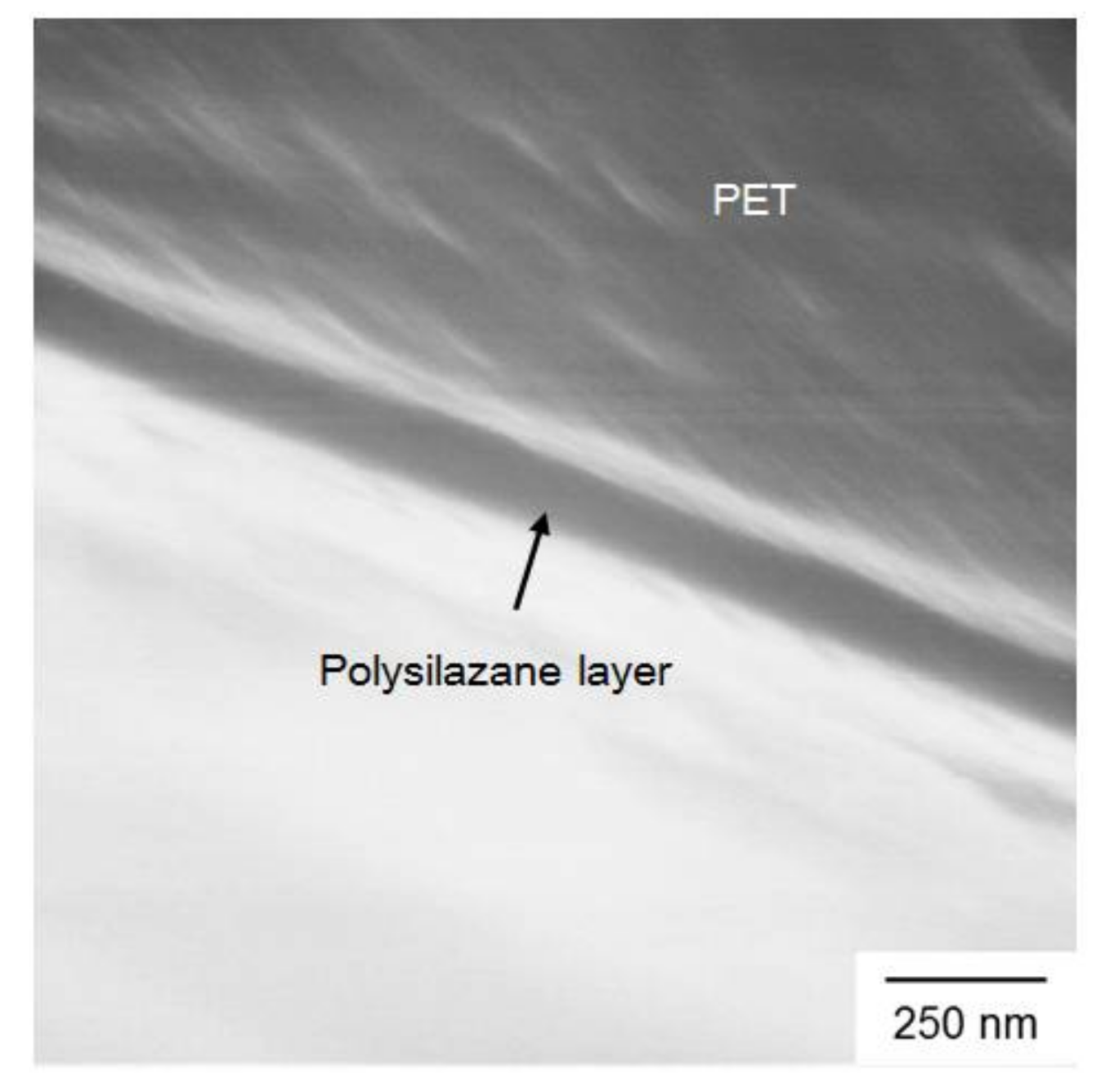
The high-performance barrier thin film used in this study is produced by LINTEC Corporation (Tokyo, Japan), and supplied by LINTEC Advanced Technologies (Kaohsiung, Taiwan). As listed in the product specifications, WVTR of this barrier thin film is 5 × 10⁻⁴ g/m2/day [32]. Following a patent of LINTEC Corporation [33], a polysilazane compound was spin-coated on a 50-μm-thick PET substrate, and heated at 120 °C for 1 min to form a 150-nm-thick polysilazane layer. A plasma ion implantation apparatus was employed to implant argon (Ar) ions into the polysilazane layer to form a gas barrier layer [33]. The barrier thin films were received in a form of A4 sheets with a thickness of about 50 μm including a 50-μm-thick PET substrate and a 150-nm-thick polysilazane layer, as shown in Figure 1. Square specimens in dimensions of 20 mm × 20 mm are cut out of the as-received sheets to perform bending tests.
2.2. Static Bending Test
In order to investigate the effect of flexural deformation on the encapsulation properties of the given barrier film, static bending tests are conducted, as shown in Figure 2. Each sample is firstly covered by two plastic sheets to keep the surface of barrier film clean. An adhesive tape is then used to attach the sample onto a cylinder of a selected radius (5, 10, or 20 mm), producing a compressive or tensile stress on the barrier layer, as shown in Figure 2. As the specimen is bent in a convex upward state (Figure 2), the gas barrier thin layer is subjected to tensile flexural stress at the top position. When the gas barrier thin layer is placed at the bottom, it is subjected to compressive flexural stress. The flexural strain is calculated according to the mechanics equations given in [29]. The maximum tensile flexural strains at the bending radii of 20, 10, and 5 mm are calculated as 1.262 × 10⁻³ mm/mm, 2.523 × 10⁻³ mm/mm, and 5.046 × 10⁻³ mm/mm, respectively. It indicates that flexural strain in the barrier layer increases with a decrease in bending radius. In such static bending tests, the investigated specimens are bent with a curvature radius of 5, 10, or 20 mm for 1, 10, 100, or 1000 h at room temperature. After static bending test, moisture-blocking performance of the sample is evaluated using a Ca corrosion test to determine the WVTR value.
2.3. WVTR Test
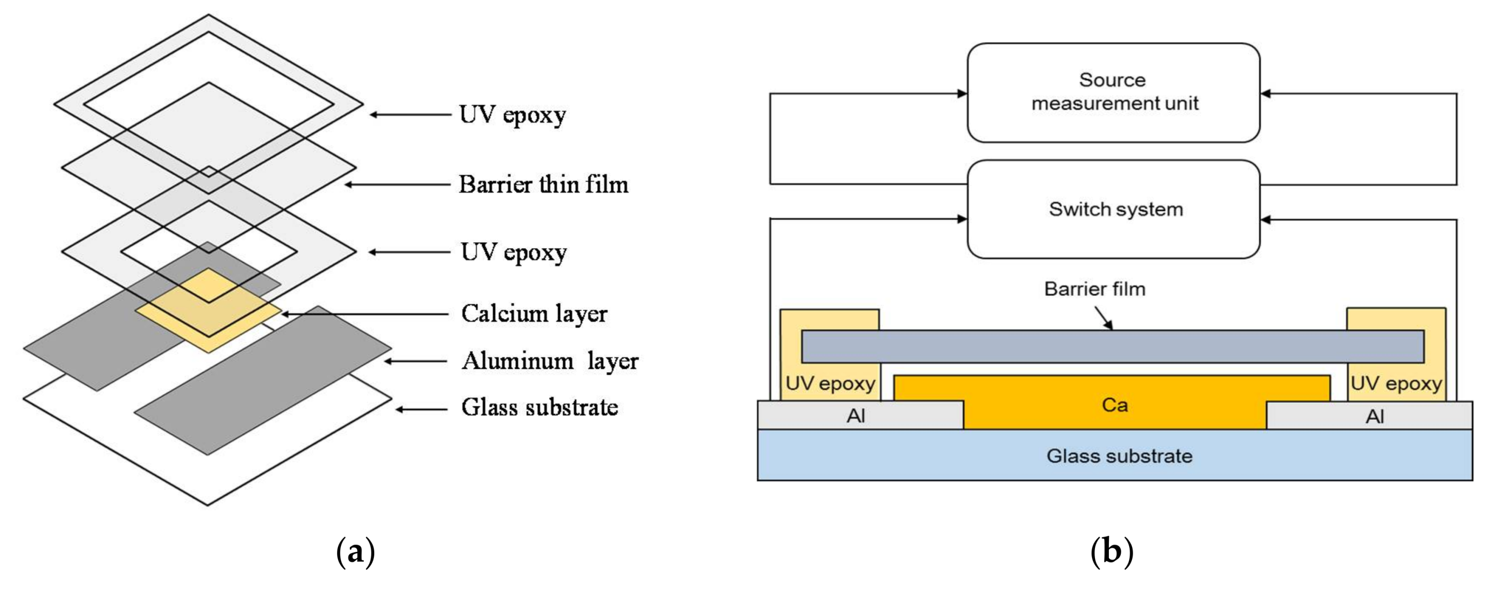
After the static bending test, an electrical Ca corrosion test is employed to measure the WVTR, as shown in Figure 3. Flexible barrier specimens which have been subjected to a certain time period of static loading were dried at 80 °C for about 30 min and transferred to a glove box system to fabricate Ca sensors. Note that glass is assumed as an impassable substance. Thus, glass substrate is capable of preventing significant moisture passing through it for a long period of ambient moisture immersion. It is applied as a protective substrate in the Ca corrosion test, as shown in Figure 3. 1-mm-thick glass substrates were firstly cut into 25 mm × 25 mm pieces. After being carefully cleaned and degassed at 120 °C for about 15 min, each glass substrate was put into the glove box system. Applying a thermal evaporation approach, a 100-nm-thick Al layer was uniformly deposited onto the glass substrate to serve as Ca sensor electrodes. In addition to depositing an Al film, the glass substrate was covered at the center with a Ca layer of 250-nm thickness. To attach the flexible barrier specimen to the Ca-Al-deposited sensor, a UV epoxy (UV epoxy-EPO-TEK®OG142, Epoxy Technology, Inc., Billerica, MA, USA) was pasted at the edges of the barrier film to bond with the Al layer using a UV-curing light source. To avoid the unwanted influence of ambient environment which may damage the Ca sensor, all the preparation processes of Ca sensor were performed in a glove box system with a water vapor less than 10 ppm. Before taking out the Ca sensors from the glove box, all of them were sealed in Al foil bags and then shipped to another laboratory to measure WVTR value. This approach of storage and shipping of Ca sensor follows the procedures given in the study of Subbarao et al. [34].
The Ca sensors were moved to an environmental chamber (GTH-080ST-SP, Giant Force Instrument Enterprise Co., Ltd., Taipei, Taiwan) and tested in a stably controlled environment of 40 °C and 90% RH. For measuring electrical resistance change of these Ca sensors, a source measurement unit combined with a homemade switch system was employed, as shown in Figure 3b. A commonly used two-point electrical resistance measurement method [10,21,23,24,35] was employed to measure the electrical resistance change in Ca sensors. The electrical current, which flowed through each Ca sensor, was continuously recorded by the source measurement unit under a constant source voltage of 20 mV. A sampling rate of once every 10 min was set to record the electrical current data.
The principle of electrical Ca test is derived from the electrical transformation of Ca corrosion [36]. Chemical reactions of Ca with water vapor and oxygen make Ca become calcium oxide or calcium hydroxide [36]. During the reactions, Ca simultaneously transforms from an opaque and conductive state to a transparent and insulating one, so WVTR value can be determined through such reactions. A schematic diagram and a photograph of the Ca-sensor layout for WVTR measurement are shown in Figure 4. A 250-nm-thick Ca sensor of an area of 10 mm × 10 mm is used to measure the WVTR value. The WVTR value can be determined from the slope of the conductance curve versus time [36]. The equation used to determine WVTR value is expressed as [10]:
where P is the WVTR, n is the molar equivalent of the degradation reaction of Ca with water vapor, M is the molar mass of the reactive elements (moisture and Ca), δ is the Ca density, ρ is the Ca resistivity, l and b are the length and width of the Ca layer, respectively, R is the resistance of Ca, d(1/R)/dt is the slope of the fitted conductance curve 1/R versus time t, and ACa/AB is the ratio of aperture, which is the ratio of the area of Ca layer over the water vapor permeation window. This technique has been employed and validated as an effective method in our previous study [35] for quantitative measurement of WVTR of the given barrier thin film. More details of WVTR measurement by this Ca corrosion test can be found in [35].
2.4. Microstructural Analysis
To determine thickness of the barrier films studied, some specimens were cut along the thickness direction to observe the cross-sectional microstructure using a scanning electron microscope (SEM) (Hitachi S-800, Hitachi, Ltd., Tokyo, Japan). After mechanical test, fracture surfaces of the barrier film specimens were observed using an optical microscope (OM) (BX60M, Olympus Corp., Tokyo, Japan) and SEM to characterize the failure mechanism. Following these analyses, the microstructural changes, interfacial cracks, and bonding defects are correlated with the WVTR change for the mechanically bent specimens.
3. Finite Element Model
In our previous study [35], a 3D FEM model was developed to simulate water vapor ingress through the barrier thin film. The 3D FEM model is applied to simulate Ca corrosion measurement in the present study. In order to compute the expected WVTR of the given barrier film after long-term static bending test, another 3D FEM model with a certain number of uniformly-spaced cracks in the coating barrier layer was constructed in this study, as shown in Figure 5. Note that the crack density is defined as number of cracks per specimen width. The built 3D FEM model consists of two layers, namely a coating barrier film (tc = 150 nm) and a PET substrate (tp = 50 μm). Values of the length and width (L = W = 1000 μm) of the 3D FEM model are set as shown. The boundary conditions of moisture concentration are applied on the top (Cz [t ≥ 0, h] = C0) and the bottom (Cz [t ≥ 0, 0] = 0) surfaces of the given model (Figure 5). An initially dry condition of moisture (Cz [0, z] = 0) in the model is assumed. Details of modeling technique and material properties are given in [35] in which the water vapor transmission mechanism follows the Fickian laws [37].
4. Results and Discussion
4.1. Effect of Static Bending
To ensure the performance reliability of the given barrier film, WVTR of the as-received barrier film is evaluated for two specimens before conducting the static bending tests. WVTR values determined for these specimens are 8 × 10⁻⁵ and 4.6 × 10⁻⁴ g/m2/day giving an average value of 2.7 × 10⁻⁴ g/m2/day which is close to that (5 × 10⁻⁴ g/m2/day) in the vendor’s data sheet [32]. Scattering in these two WVTR values may be attributed to the difference in specimen batch of fabrication and preparation. In order to determine bending effect on the WVTR of the given barrier film, two bending stress states are considered, namely compressive and tensile bending stresses. At first, the WVTR values are determined to be 8 × 10⁻⁵ and 2 × 10⁻⁴ g/m2/day, respectively, under tensile and compressive bending of a 20-mm curvature radius for 1000 h. These WVTR values are comparable with those of as-received barrier film indicating that bending with a curvature radius of 20 mm does not deteriorate the barrier film’s performance at all.
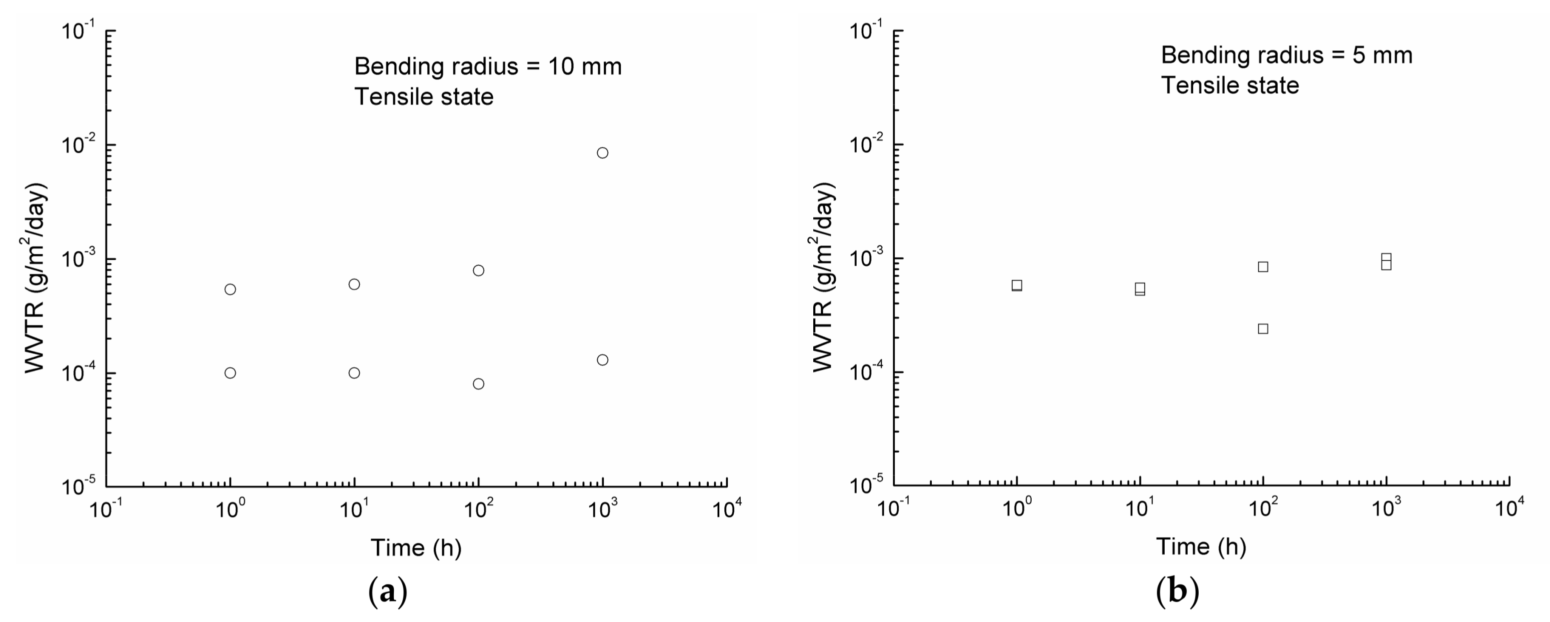
The change of WVTR with time under tensile bending at two radii of curvature is shown in Figure 6. Note that two specimens were repeatedly tested for each given bending condition, one showing a higher WVTR value and the other showing a lower WVTR value. As shown in Figure 6a, the higher WVTR values under tensile bending with a 10-mm curvature radius are 5.4 × 10⁻⁴, 6 × 10⁻⁴, 7.9 × 10⁻⁴, and 8.5 × 10⁻³ g/m2/day for 1, 10, 100, and 1000 h of bending, respectively. The lower counterpart values are 1 × 10⁻⁴, 1 × 10⁻⁴, 8 × 10⁻⁵, and 1.3 × 10⁻⁴ g/m2/day for 1, 10, 100, and 1000 h of bending, respectively. Compared with the WVTR values of as-received barrier film, these WVTR values show that tensile bending could significantly increase the WVTR to 8.5 × 10⁻³ g/m2/day after bending with a 10-mm curvature radius for 1000 h. However, for a similar tensile bending state with a shorter loading time such as 1, 10, and 100 h, no significant change of WVTR is found, compared to the as-received barrier film. As shown in Figure 6b, the higher WVTR values under tensile bending with a 5-mm curvature radius are 5.8 × 10⁻⁴, 5.5 × 10⁻⁴, 8.4 × 10⁻⁴, and 1 × 10⁻³ g/m2/day for 1, 10, 100, and 1000 h of bending, respectively. The lower counterpart values are 5.7 × 10⁻⁴, 5.2 × 10⁻⁴, 2.4 × 10⁻⁴, and 8.7 × 10⁻⁴ g/m2/day for 1, 10, 100, and 1000 h, respectively. Comparison of these values with those of as-received barrier film indicates that an effect of tensile bending is also found for bending at a 5-mm curvature radius for 1000 h, as the WVTR increases to a value of 1 × 10⁻³ g/m2/day. Similar to that of 10-mm curvature radius, no significant effect of tensile bending is observed for 5-mm curvature radius with a short loading time of 1, 10, and 100 h. These results reveal that tensile bending effect on the WVTR of barrier film takes place after a long period of time (1000 h) for the given radii of bending curvature.
Variation of the WVTR with time under compressive bending at two radii of curvature is shown in Figure 7. As shown in Figure 7a, the higher WVTR values under compressive bending with a 10-mm curvature radius are 6 × 10⁻⁴, 7.5 × 10⁻⁴, 6 × 10⁻⁴, and 4 × 10⁻⁴ g/m2/day for 1, 10, 100, and 1000 h, respectively. The lower counterpart values are 1.7 × 10⁻⁴, 2 × 10⁻⁴, 1.2 × 10⁻⁴, and 2 × 10⁻⁴ g/m2/day for 1, 10, 100, and 1000 h, respectively. No significant detriment to the WVTR of barrier film is found for compressive bending with a radius of curvature of 10 mm. The WVTR values for all of the given periods of bending are comparable with those of as-received barrier film. As shown in Figure 7b, the higher WVTR values under compressive bending with a 5-mm curvature radius are 7.7 × 10⁻⁴, 7 × 10⁻⁴, 8.4 × 10⁻⁴, and 6 × 10⁻⁴ g/m2/day for 1, 10, 100, and 1000 h, respectively. The lower counterpart values are 3 × 10⁻⁴, 5.5 × 10⁻⁴, 7.6 × 10⁻⁴, and 7 × 10⁻⁵ g/m2/day for 1, 10, 100, and 1000 h, respectively. Similarly, a compressive bending of 5-mm curvature radius does not change the WVTR value significantly up to a bending time of 1000 h.
In comparison of Figure 6a and Figure 7a, WVTR of the barrier film is increased under tensile bending with a bending radius of 10 mm for 1000 h, but it remains stable under compressive bending with a similar bending radius for 1000 h. When the bending radius is reduced to 5 mm, a similar phenomenon is also observed. These results reveal that tensile bending is more detrimental than compressive bending to the moisture-blocking performance under a long-term static flexural deformation. However, given a tensile bending time, the lower WVTR value measured for 5-mm curvature radius is greater than the counterpart of 10-mm curvature radius. It indicates that tensile bending at a 5-mm radius is more damaging than a 10-mm one. As described in Section 2.2, the flexural strain caused by bending deformation increases with a decrease in bending radius. These results reveal that bending such barrier thin film with a smaller radius of curvature in a certain period of time apparently generates a larger amount of damage leading to an increase in WVTR.
4.2. Failure Analysis
As pinholes and microcracks serve as the major path and dominate the water permeation process in the barrier film, corrosion process in the Ca sensor may not take place homogeneously as a result of a non-uniform distribution of such defects. Therefore, the slope of the fitted conductance curve in the steady state represents an average moisture permeation rate. In other words, WVTR determined by Ca corrosion method only estimates how much moisture gets through the permeation window of the barrier film, but it cannot show what the types and quantity of moisture permeation path are. In order to investigate how the WVTR is affected by the bending deformation, surface morphology of the as-received and statically bent barrier specimens is observed using OM and the results are shown in the following.
An OM micrograph of an as-received barrier film is shown in Figure 8, which reveals some randomly distributed veins. These randomly distributed veins are present in every barrier film and are presumably formed in the fabrication process. As described in the previous section, for a bending radius of 5 and 10 mm, no significantly detrimental effect is found for tensile bending up to 100 h and for compressive bending up to 1000 h. Exemplified OM micrographs of these bent specimens are given for comparison with the as-received one. Figure 9 shows the OM micrographs of the barrier films after tensile bending with a 5-mm and a 10-mm curvature radius for 100 h. OM micrographs of the barrier films after compressive bending with a 5-mm and a 10-mm curvature radius for 1000 h are shown in Figure 10. Morphologies of these bent barrier films (Figure 9 and Figure 10) are almost the same as those of the as-received barrier film (Figure 8). This is consistent with the WVTR measurements which do not significantly change under these bending conditions.
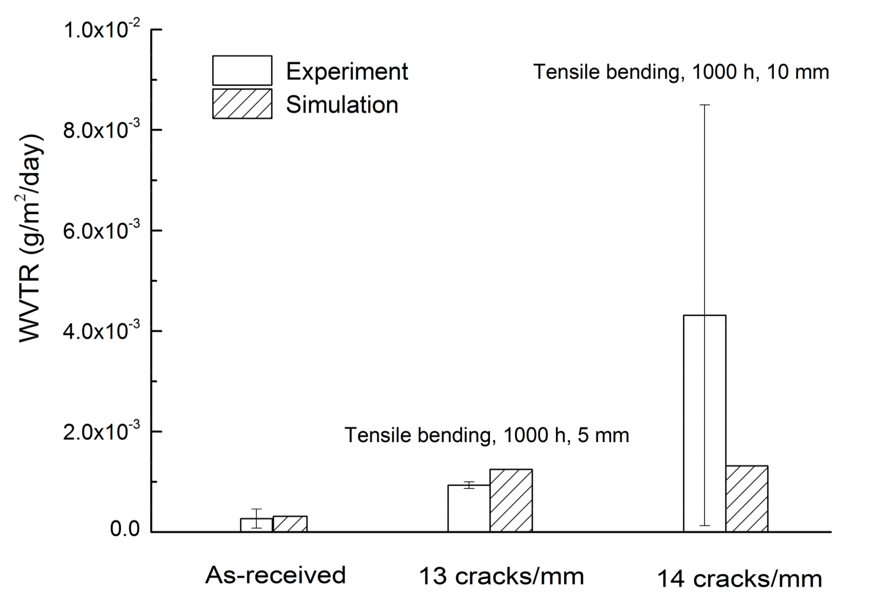
As mentioned in Section 4.1, the highest WVTR values of the barrier film are about 8.5 × 10⁻³ and 1 × 10⁻³ g/m2/day when subjected to tensile bending of a radius of 10 and 5 mm for 1000 h, respectively. OM micrographs of these two barrier films are shown in Figure 11. As shown in Figure 11a, cracks are found in the barrier film after tensile bending of a radius of 10 mm for 1000 h. These cracks are perpendicular to the direction of applied stress, roughly parallel to each other, and appear as straight lines, as expected. The average crack density in the barrier film is about 14 cracks/mm, as shown in Figure 11a. Similarly, Figure 11b shows the formation of cracks in the barrier film after tensile bending of a radius of 5 mm for 1000 h. Again, these straight cracks are perpendicular to the loading direction and parallel to each other. The average crack density in the barrier film is about 13 cracks/mm, as shown in Figure 11b. These cracks could serve as pathways for water vapor to penetrate through the barrier film. However, cracks do not appear in every specimen after tensile bending with a radius of 10 mm or 5 mm for 1000 h. For example, the lower WVTR value in tensile bending with a 10-mm curvature radius is 1.3 × 10⁻⁴ g/m2/day after 1000 h of bending, as shown in Figure 6a. These specimens do not exhibit visible damage under OM and their WVTR values do not significantly increase, either. The possible reason is that cracks might develop at pre-existing defects and lead to the rupture under bending [38,39]. As the pre-existing defects are not evenly distributed in the barrier film and the number of defects might vary with sample, they would influence the probability of crack formation and are responsible for the scattering in WVTR data.
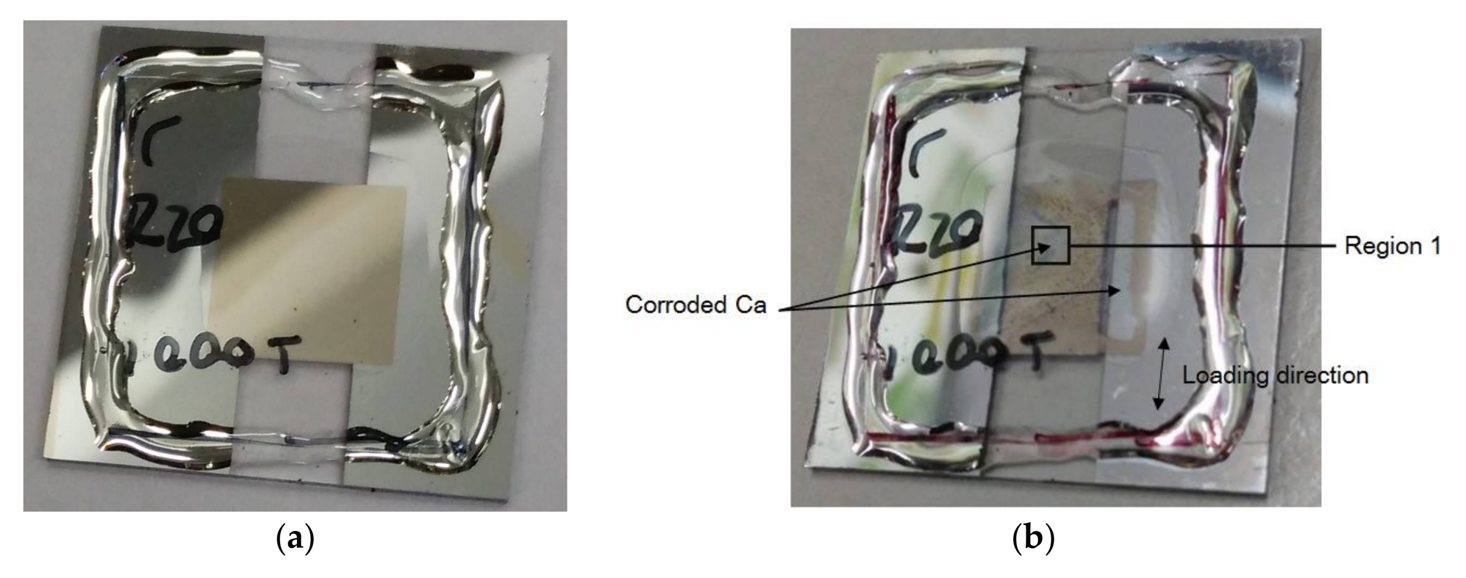
To clarify the scattering of WVTR data for a repeated bending condition, a specimen under tensile bending of a 20-mm curvature radius for 1000 h, of which the WVTR value is 8 × 10⁻⁵ g/m2/day, is taken as an example to show the Ca corroding process. As shown in Figure 12, a Ca sensor is covered by the barrier film. In comparison of Figure 12a,b, this Ca sensor is partially corroded by water vapor at 40 °C and 90% RH after 610 h. As the partially corroded area in the Ca sensor is not perpendicular to the loading direction, it is confirmed again that no cracks are formed to deteriorate the barrier film’s performance. The OM micrograph of Region 1 in the corroded area of Figure 12b is shown in Figure 12c. It shows that water readily penetrate the barrier film through pre-existing defects such as pinholes. As shown in Figure 12c, the pinhole defects are not homogenously distributed in the barrier film. In other words, WVTR of the barrier film at various zones may be different. Because the tested samples in physical dimensions of 2 mm × 2 mm are cut out from the A4 sheets, the initial defect population in each sample may not be the same. Therefore, scattering of the WVTR data for each repeated bending condition is not avoided in the present study.
4.3. Numerical Analysis
In this study, crack densities of 13 and 14 cracks/mm are separately established in the 3D FEM model to compute the expected WVTR of the given barrier film. Note that these crack densities considered in the 3D FEM model are observed in the OM micrographs of mechanically bent barrier specimens (Figure 11). As described in Section 4.2, these cracks serve as major pathways for moisture to diffuse through the barrier thin film. They lead to an increase in WVTR of the barrier thin film. The expecting WVTR of the 3D FEM barrier model is then calculated to make a comparison with the experimental results. The simulation of WVTR variation as a function of moisture exposure time for the as-received and damaged barrier specimens is shown in Figure 13. As shown in Figure 13, WVTR of the damaged barrier film significantly increases due to presence of cracks. Apparently, a larger crack density results in a higher WVTR (Figure 13). As expected, accumulation of cracking leads to an increase in WVTR of barrier film as a result of an increase in moisture exposure area and entrances. The comparison between numerical and experimental results of WVTR is shown in Figure 14. The average value of WVTR is represented by the height of a certain column and the maximum and minimum WVTR values correspond to the ends of each error bar (Figure 14). As shown in Figure 14, the WVTR values computed using the 3D FEM cracking model agree with the experimental results. The numerical results indicate that the 3D FEM model can be used to predict the WVTR change of a barrier film based on the identified crack density. The 3D FEM model developed shows a good quantitative validation for such a failure mechanism. The present findings of this study could provide an insight into the improvement of encapsulation performance and prevention of damage development of such barrier film.
5. Conclusions
The durability of a commercial barrier film is investigated under static bending and the relevant WVTR value is measured at 40 °C and 90% RH. Using a 3D FEM model, the expected WVTR is calculated and compared with the experimental results. Conclusions of the WVTR measurement, fractography, and numerical results are drawn below.
- For both tensile and compressive bending of a 20-mm curvature radius, WVTR values are stable for 1000 h. Bending with a radius of 20 mm does not deteriorate the barrier film’s performance.
- For tensile bending of 10-mm and 5-mm curvature radii, no significant change of WVTR is found for a shorter loading period such as 1, 10, and 100 h. However, tensile bending effect on the WVTR of the given barrier film takes place after a long period of loading (1000 h) for these two radii of bending curvature.
- For compressive bending of both 10-mm and 5-mm curvature radii, WVTR values are stable for up to 1000 h of static loading.
- Pinholes and microcracks are found and serve as the major pathways for water vapor in the barrier film. A non-uniform distribution of defects is found in the barrier film and responsible for the scattering of data in WVTR measurement.
- Numerical analyses show that there are significant increases in WVTR as a result of cracking in the barrier thin film. It corresponds to an apparent increase in moisture entrances.
- The WVTR values calculated by the 3D FEM model are in good agreement with the experimental results considering a similar crack density observed. The 3D FEM model established is applicable to calculate the WVTR change associated with cracking in the barrier thin film.
Acknowledgments
This work was supported by the Ministry of Science and Technology (Taiwan) under contract no. MOST 105-2221-E-008-017-MY3.
Author Contributions
Chih-Kuang Lin and Hung-I Lu conceived and designed the experiments; Hung-I Lu and Bao-Dong To performed the experiments; Dinh-Phuc Tran performed the numerical analysis; Hung-I Lu, Chih-Kuang Lin, and Dinh-Phuc Tran analyzed the data; Hung-I Lu, Chih-Kuang Lin, and Dinh-Phuc Tran wrote the paper.
Conflicts of Interest
The authors declare no conflict of interest.
References
- Søndergaard, R.R.; Hösel, M.; Krebs, F.C. Roll-to-Roll fabrication of large area functional organic materials. J. Polym. Sci. B Polym. Phys. 2013, 51, 16–34. [Google Scholar] [CrossRef]
- Yoo, S.-I.; Yoon, J.-A.; Kim, N.-H.; Kim, J.-W.; Kang, J.-S.; Moon, C.-B.; Kim, W.-Y. Improvement of efficiency roll-off in blue phosphorescence OLED using double dopants emissive layer. J. Lumin. 2015, 160, 346–350. [Google Scholar] [CrossRef]
- Kim, H.-S.; Moon, S.-I.; Hwang, D.-E.; Jeong, K.-W.; Kim, C.-K.; Moon, D.-G.; Hong, C. Novel fabrication method of microlens arrays with high OLED outcoupling efficiency. Opt. Laser Technol. 2016, 77, 104–110. [Google Scholar] [CrossRef]
- Zhou, J.; Ai, N.; Wang, L.; Zheng, H.; Luo, C.; Jiang, Z.; Yu, S.; Cao, Y.; Wang, J. Roughening the white OLED substrate’s surface through sandblasting to improve the external quantum efficiency. Org. Electron. 2011, 12, 648–653. [Google Scholar] [CrossRef]
- Sun, Q.; Li, D.; Dong, G.; Jin, X.; Duan, L.; Wang, L.; Qiu, Y. Improved organic optocouplers based on a deep blue fluorescent OLED and an optimized bilayer heterojunction photosensor. Sens. Actuator B Chem. 2013, 188, 879–885. [Google Scholar] [CrossRef]
- Lee, J.-H.; Wu, M.-H.; Chao, C.-C.; Chen, H.-L.; Leung, M.-K. High efficiency and long lifetime OLED based on a metal-doped electron transport layer. Chem. Phys. Lett. 2005, 416, 234–237. [Google Scholar] [CrossRef]
- Kang, J.-S.; Yoon, J.-A.; Yoo, S.-I.; Kim, J.-W.; Yi, S.; Zhu, F.; Cheah, K.-W.; Kim, W.-Y. Luminous efficiency enhancement in blue phosphorescent organic light-emitting diodes with an electron confinement layers. Opt. Mater. 2015, 47, 78–82. [Google Scholar] [CrossRef]
- Oh, M.-C.; Park, J.-H.; Jeon, H.-J.; Go, J.-S. Hollow-core polymeric nanoparticles for the enhancement of OLED outcoupling efficiency. Displays 2015, 37, 72–78. [Google Scholar] [CrossRef]
- Yang, Q.; Hao, Y.; Wang, Z.; Li, Y.; Wang, H.; Xu, B. Double-emission-layer green phosphorescent OLED based on LiF-doped TPBi as electron transport layer for improving efficiency and operational lifetime. Synth. Met. 2012, 162, 398–401. [Google Scholar] [CrossRef]
- NREL’s e-Ca Test. NREL. Available online: http://www.nrel.gov/docs/fy13osti/56665.pdf (accessed on 11 January 2016).
- Riedl, T.; Winkler, T.; Schmidt, H.; Meyer, J.; Schneidenbach, D.; Johannes, H.H.; Kowalsky, W.; Weimann, T.; Hinze, P. Reliability aspects of organic light emitting diodes. In Proceedings of the 2010 IEEE International Reliability Physics Symposium (IRPS), Garden Grove, CA, USA, 2–6 May 2010; pp. 327–333. [Google Scholar]
- Thinness, Strength, and Bend-Ability Render Visions of Wrap-Around Displays, Corning. Available online: https://www.corning.com/worldwide/en/products/display-glass/products/corning-willow-glass.html (accessed on 11 January 2016).
- Park, J.-S.; Chae, H.; Chung, H.-K.; Lee, S.-I. Thin film encapsulation for flexible AM-OLED: A review. Semicond. Sci. Technol. 2011, 26, 034001. [Google Scholar] [CrossRef]
- Lewis, J. Material challenge for flexible organic devices. Mater. Today 2006, 9, 38–45. [Google Scholar] [CrossRef]
- Wong, W.S.; Salleo, A. Flexible Electronics: Materials and Applications; Springer Publishing Company: New York, NY, USA, 2009. [Google Scholar]
- Da Silva Sobrinho, A.S.; Latrèche, M.; Czeremuszkin, G.; Klemberg-Sapieha, J.E.; Wertheimer, M.R. Transparent barrier coatings on polyethylene terephthalate by single- and dual-frequency plasma-enhanced chemical vapor deposition. J. Vac. Sci. Technol. A 1998, 16, 3190–3198. [Google Scholar] [CrossRef]
- Han, Y.-C.; Kim, E.; Kim, W.; Im, H.-G.; Bae, B.-S.; Choi, K.-C. A flexible moisture barrier comprised of a SiO2-embedded organic–inorganic hybrid nanocomposite and Al2O3 for thin-film encapsulation of OLEDs. Org. Electron. 2013, 14, 1435–1440. [Google Scholar] [CrossRef]
- Carcia, P.F.; McLean, R.S.; Reilly, M.H.; Groner, M.D.; George, S.M. Ca test of Al2O3 gas diffusion barriers grown by atomic layer deposition on polymers. Appl. Phys. Lett. 2006, 89, 031915. [Google Scholar] [CrossRef]
- Majee, S.; Cerqueira, M.F.; Tondelier, D.; Vanel, J.C.; Geffroy, B.; Bonnassieux, Y.; Alpuim, P.; Bourée, J.E. Permeation barrier performance of hot wire-CVD grown silicon-nitride films treated by argon plasma. Thin Solid Films 2015, 575, 72–75. [Google Scholar] [CrossRef] [Green Version]
- Turak, A. Interfacial degradation in organic optoelectronics. RSC Adv. 2013, 3, 6188–6225. [Google Scholar] [CrossRef]
- Lee, S.; Choi, H.; Shin, S.; Park, J.; Ham, G.; Jung, H.; Jeon, H. Permeation barrier properties of an Al2O3/ZrO2 multilayer deposited by remote plasma atomic layer deposition. Curr. Appl. Phys. 2014, 14, 552–557. [Google Scholar] [CrossRef]
- Jia, Z.; Tucker, M.B.; Li, T. Failure mechanics of organic–inorganic multilayer permeation barriers in flexible electronics. Compos. Sci. Technol. 2011, 71, 365–372. [Google Scholar] [CrossRef]
- Kim, N.; Potscavage, W.J., Jr.; Sundaramoothi, A.; Henderson, C.; Kippelen, B.; Graham, S. A correlation study between barrier film performance and shelf lifetime of encapsulated organic solar cells. Sol. Energ. Mat. Sol. Cells 2012, 101, 140–146. [Google Scholar] [CrossRef]
- Seo, S.-W.; Jung, E.; Seo, S.-J.; Chae, H.; Chung, H.-K.; Cho, S.-M. Toward fully flexible multilayer moisture-barriers for organic light-emitting diodes. J. Appl. Phys. 2013, 114, 143505. [Google Scholar] [CrossRef]
- Seo, S.-W.; Jung, E.; Chae, H.; Seo, S.-J.; Chung, H.-K.; Cho, S.-M. Bending properties of organic–inorganic multilayer moisture barriers. Thin Solid Films 2014, 550, 742–746. [Google Scholar] [CrossRef]
- Kim, E.; Han, Y.; Kim, W.; Choi, K.-C.; Im, H.-G.; Bae, B.-S. Thin film encapsulation for organic light emitting diodes using a multi-barrier composed of MgO prepared by atomic layer deposition and hybrid materials. Org. Electron. 2013, 14, 1737–1743. [Google Scholar] [CrossRef]
- Cho, A.-R.; Kim, E.-H.; Park, S.-Y.; Park, L.-S. Flexible OLED encapsulated with gas barrier film and adhesive gasket. Synth. Met. 2014, 193, 77–80. [Google Scholar] [CrossRef]
- Majee, S.; Geffroy, B.; Bonnassieux, Y.; Bourée, J.-E. Interface effects on the moisture barrier properties of SiNx/PMMA/SiNx hybrid structure. Surf. Coat. Technol. 2014, 254, 429–432. [Google Scholar] [CrossRef]
- Kim, N.; Graham, S. Development of highly flexible and ultra-low permeation rate thin-film barrier structure for organic electronics. Thin Solid Films 2013, 547, 57–62. [Google Scholar] [CrossRef]
- Kim, K.; Luo, H.; Singh, A.K.; Zhu, T.; Graham, S.; Pierron, O.N. Environmentally assisted cracking in silicon nitride barrier films on poly(ethylene terephthalate) substrates. ACS Appl. Mater. Interfaces 2016, 8, 27169–27178. [Google Scholar] [CrossRef] [PubMed]
- Kim, K.; Graham, S.; Pierron, O. Note: A single specimen channel crack growth technique applied to brittle thin films on polymer substrates. Rev. Sci. Instrum. 2017, 88, 036102. [Google Scholar] [CrossRef] [PubMed]
- LINTEC Product Information. Available online: http://www.lintec-global.com/products/ (accessed on 9 March 2018).
- Nishijima, K.; Naganawa, S.; Fuchi, E. Adhesive Agent Composition, Adhesive Sheet, and Electronic Device and Production Method Therefor. U.S Patent 20,150,299,519, 22 October 2015. [Google Scholar]
- Subbarao, S.P.; Bahlke, M.E.; Kymissis, I. Laboratory thin-film encapsulation of air-sensitive organic semiconductor devices. IEEE Trans. Electron Devices 2010, 57, 153–156. [Google Scholar] [CrossRef]
- Tran, D.-P.; Lin, C.-K.; To, B.-D. Effects of cyclic deformation on a barrier thin film for flexible organic optoelectronic devices. Thin Solid Films 2018, 650, 20–31. [Google Scholar] [CrossRef]
- Paetzold, R.; Winnacker, A.; Henseler, D.; Cesari, V.; Heuser, K. Permeation rate measurements by electrical analysis of calcium corrosion. Rev. Sci. Instrum. 2003, 74, 5147–5150. [Google Scholar] [CrossRef]
- Crank, J. The Mathematics of Diffusion, 2nd ed.; Oxford University Press: Oxford, UK, 1975. [Google Scholar]
- Sim, B.; Kim, E.-H.; Park, J.; Lee, M. Highly enhanced mechanical stability of indium tin oxide film with a thin Al buffer layer deposited on plastic substrate. Surf. Coat. Technol. 2009, 204, 309–312. [Google Scholar] [CrossRef]
- Leterrier, Y.; Médico, L.; Demarco, F.; Månson, J.A.E.; Betz, U.; Escolà, M.F.; Kharrazi Olsson, M.; Atamny, F. Mechanical integrity of transparent conductive oxide films for flexible polymer-based displays. Thin Solid Films 2004, 460, 156–166. [Google Scholar] [CrossRef]
Figure 1.
Cross-sectional SEM micrograph of the high-performance barrier film investigated.

Figure 2.
Schematic diagram of static bending test and setup.
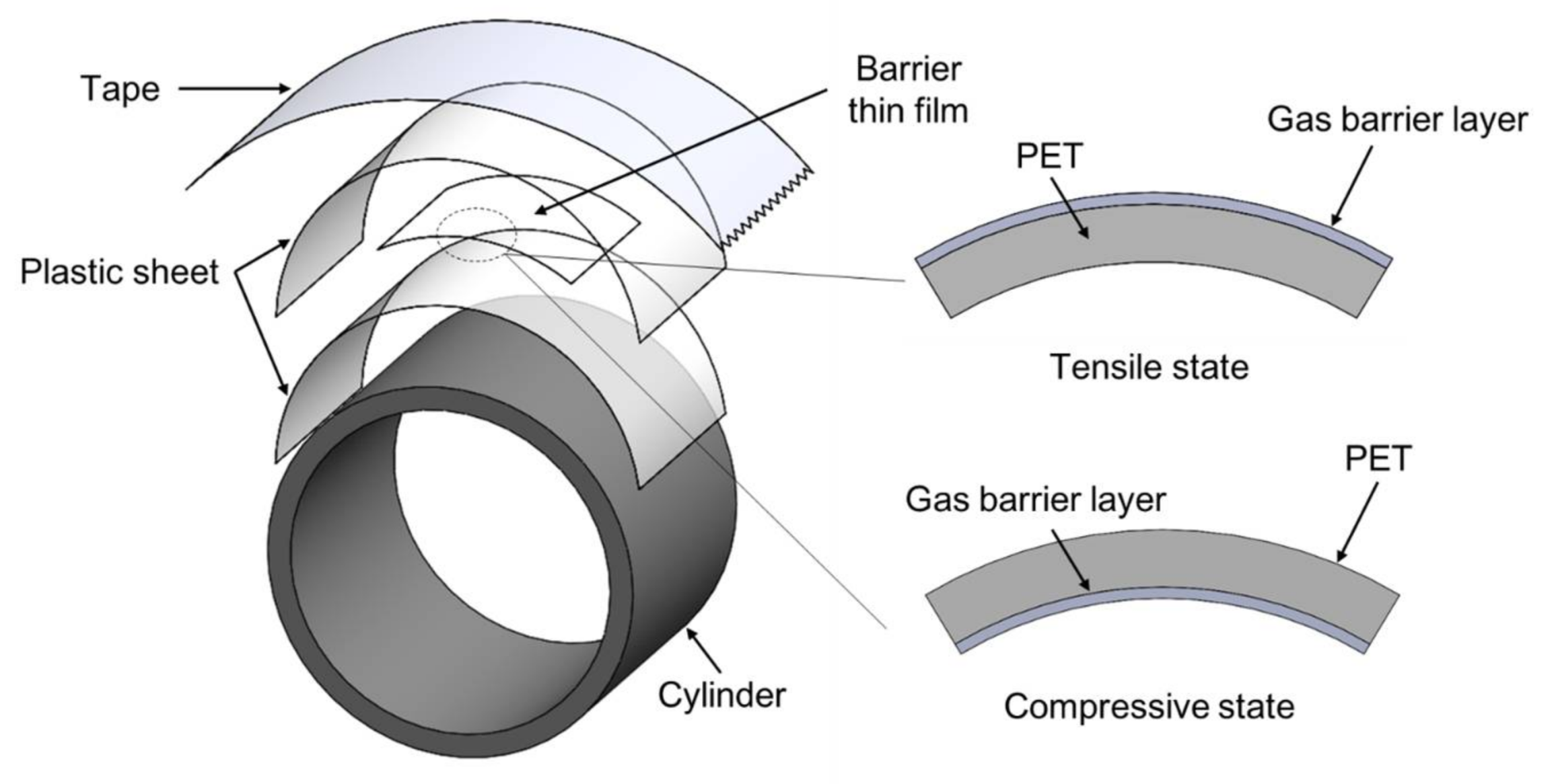
Figure 3.
Schematic diagram of WVTR measurement: (a) exploded view of Ca test layout; (b) experimental setup.
Figure 3.
Schematic diagram of WVTR measurement: (a) exploded view of Ca test layout; (b) experimental setup.

Figure 4.
(a) Schematic diagram of Ca-sensor layout for WVTR measurement of barrier film; (b) Photograph of the WVTR sample and Ca-sensor layout.
Figure 4.
(a) Schematic diagram of Ca-sensor layout for WVTR measurement of barrier film; (b) Photograph of the WVTR sample and Ca-sensor layout.
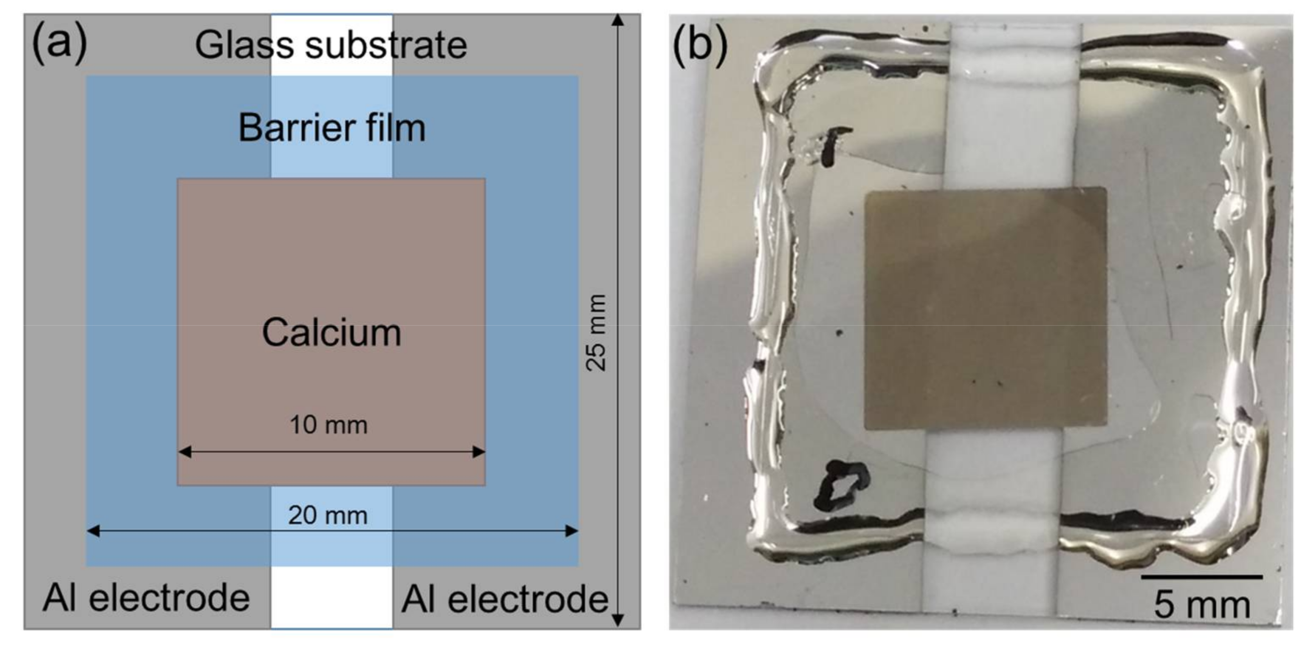
Figure 5.
Schematic diagram of a 3D FEM model with uniformly-spaced cracks in the coating barrier.
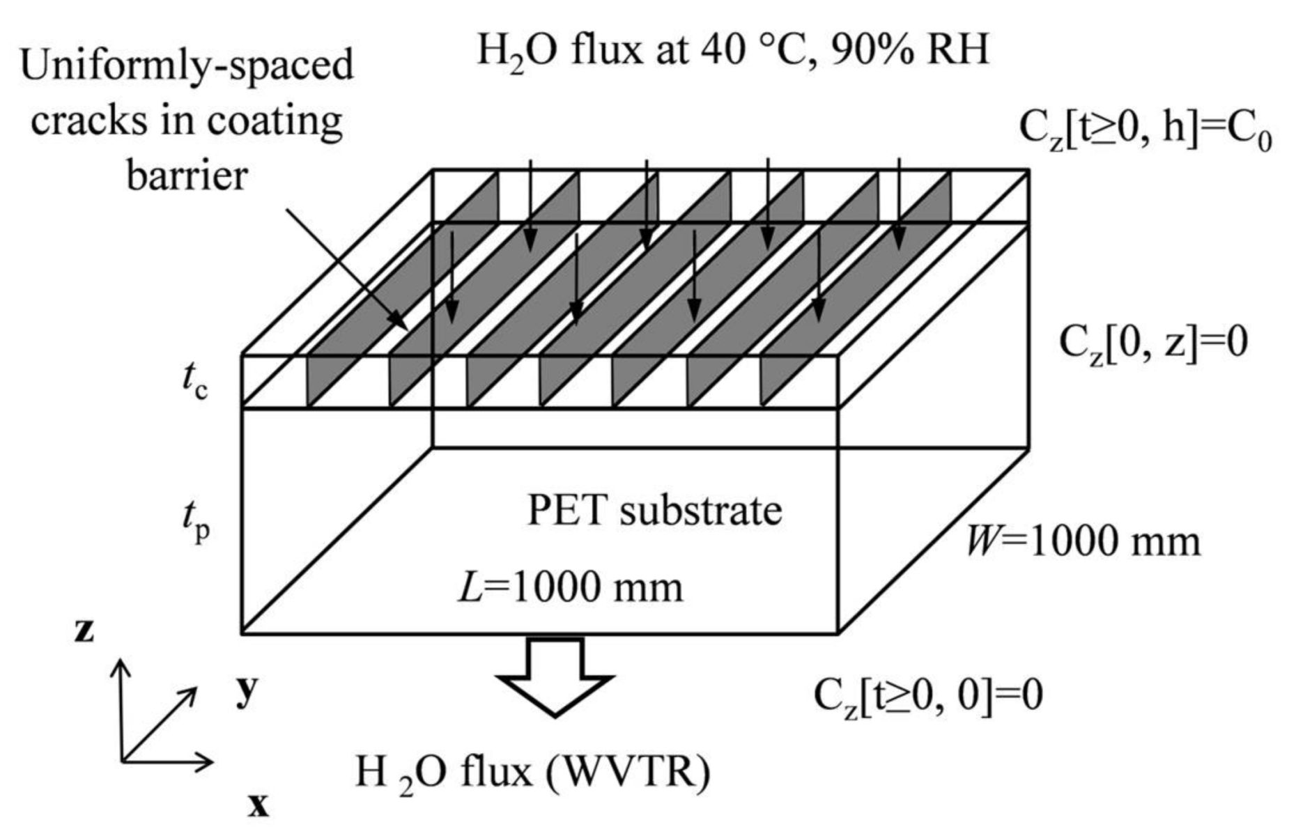
Figure 6.
WVTR change of barrier film bent in tensile state: (a) bending radius of 10 mm; (b) bending radius of 5 mm.
Figure 6.
WVTR change of barrier film bent in tensile state: (a) bending radius of 10 mm; (b) bending radius of 5 mm.

Figure 7.
WVTR change of barrier film bent in compressive state: (a) bending radius of 10 mm; (b) bending radius of 5 mm.
Figure 7.
WVTR change of barrier film bent in compressive state: (a) bending radius of 10 mm; (b) bending radius of 5 mm.
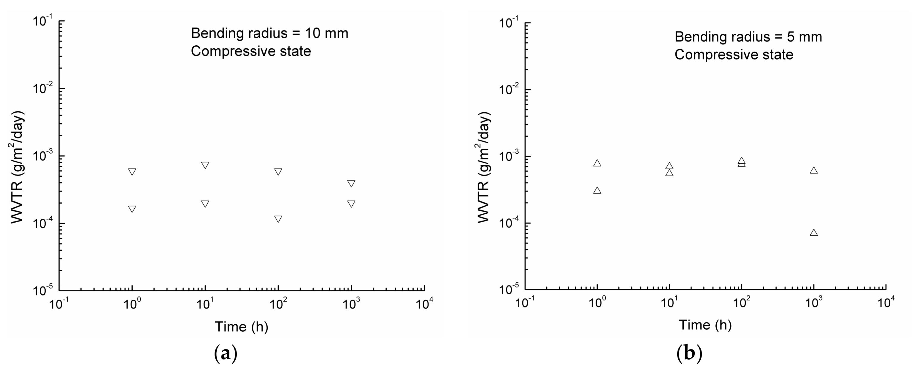
Figure 8.
OM micrograph of as-received barrier film.
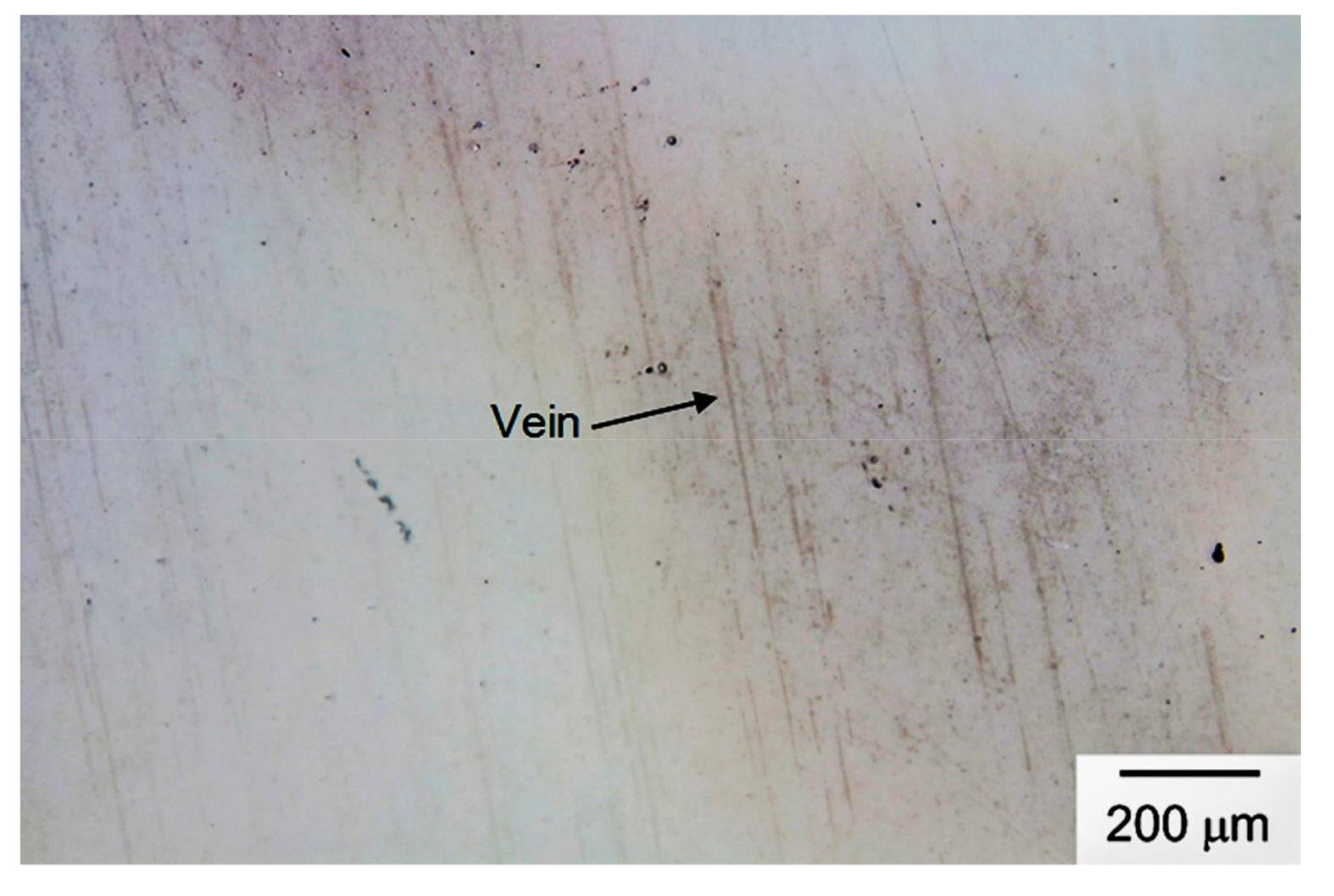
Figure 9.
OM micrographs of barrier film after tensile bending with (a) a 10-mm and (b) a 5-mm curvature radius for 100 h.
Figure 9.
OM micrographs of barrier film after tensile bending with (a) a 10-mm and (b) a 5-mm curvature radius for 100 h.

Figure 10.
OM micrographs of barrier film after compressive bending with (a) a 10-mm and (b) a 5-mm curvature radius for 1000 h.
Figure 10.
OM micrographs of barrier film after compressive bending with (a) a 10-mm and (b) a 5-mm curvature radius for 1000 h.
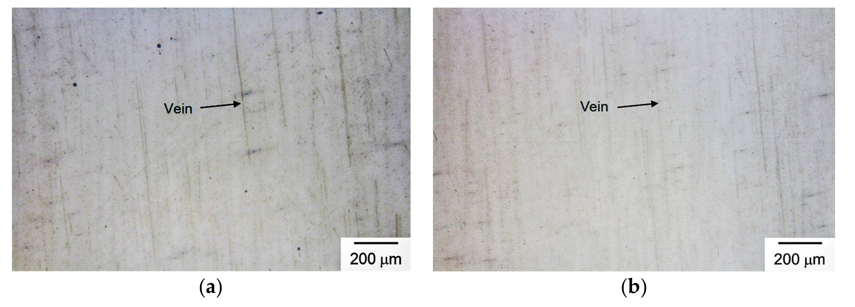
Figure 11.
OM micrographs of barrier films after tensile bending with (a) a 10-mm and (b) a 5-mm curvature radius for 1000 h.
Figure 11.
OM micrographs of barrier films after tensile bending with (a) a 10-mm and (b) a 5-mm curvature radius for 1000 h.
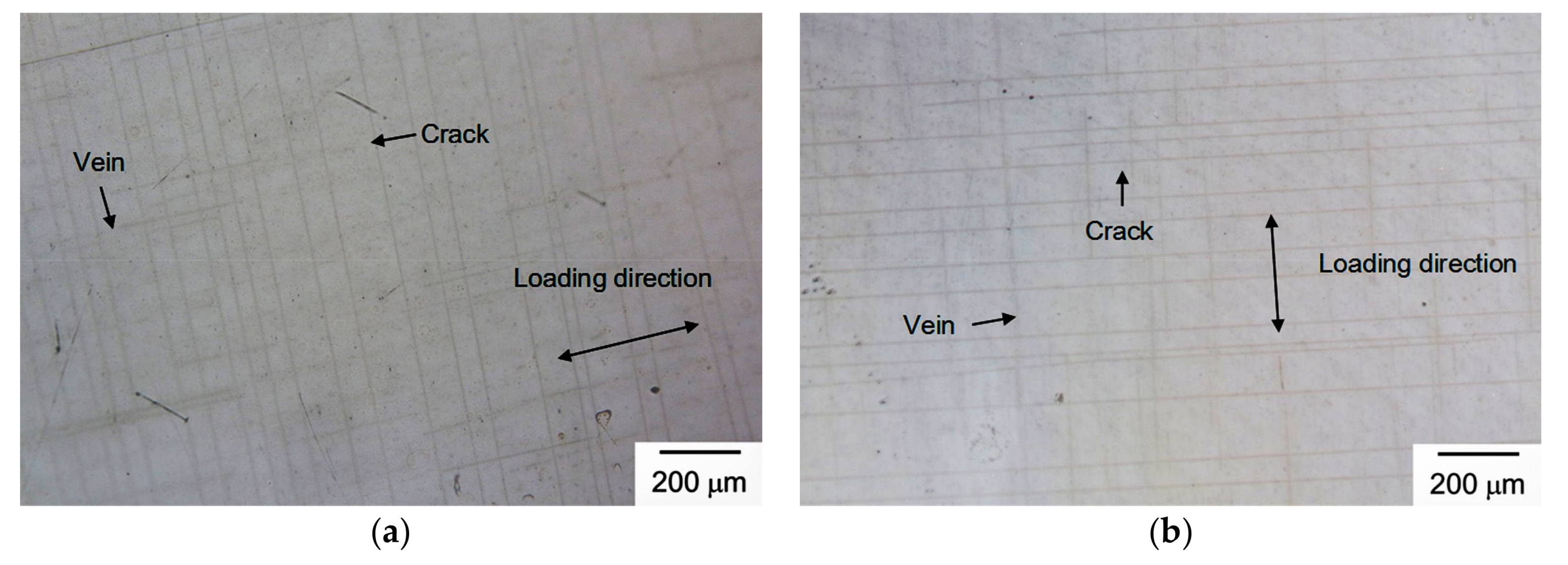
Figure 12.
Corroding of a Ca sensor covered by a barrier film after tensile bending of a 20-mm curvature radius for 1000 h: (a) as attached; (b) after 610 h; (c) OM micrograph of Region 1 in (b).
Figure 12.
Corroding of a Ca sensor covered by a barrier film after tensile bending of a 20-mm curvature radius for 1000 h: (a) as attached; (b) after 610 h; (c) OM micrograph of Region 1 in (b).

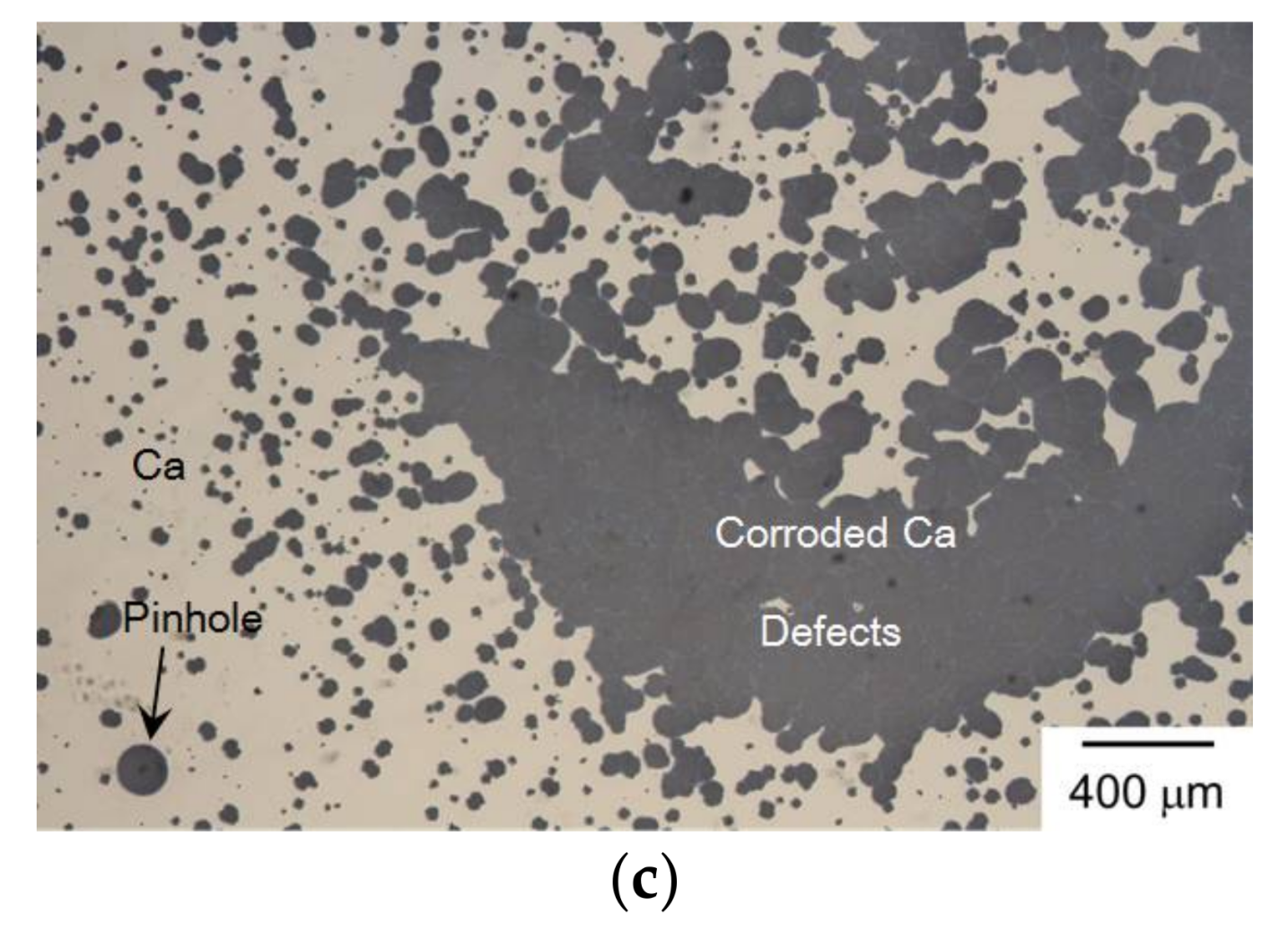
Figure 13.
Simulation of WVTR variation through the 3D FEM barrier model as a function of exposure time for the as-received and damaged cases.
Figure 13.
Simulation of WVTR variation through the 3D FEM barrier model as a function of exposure time for the as-received and damaged cases.
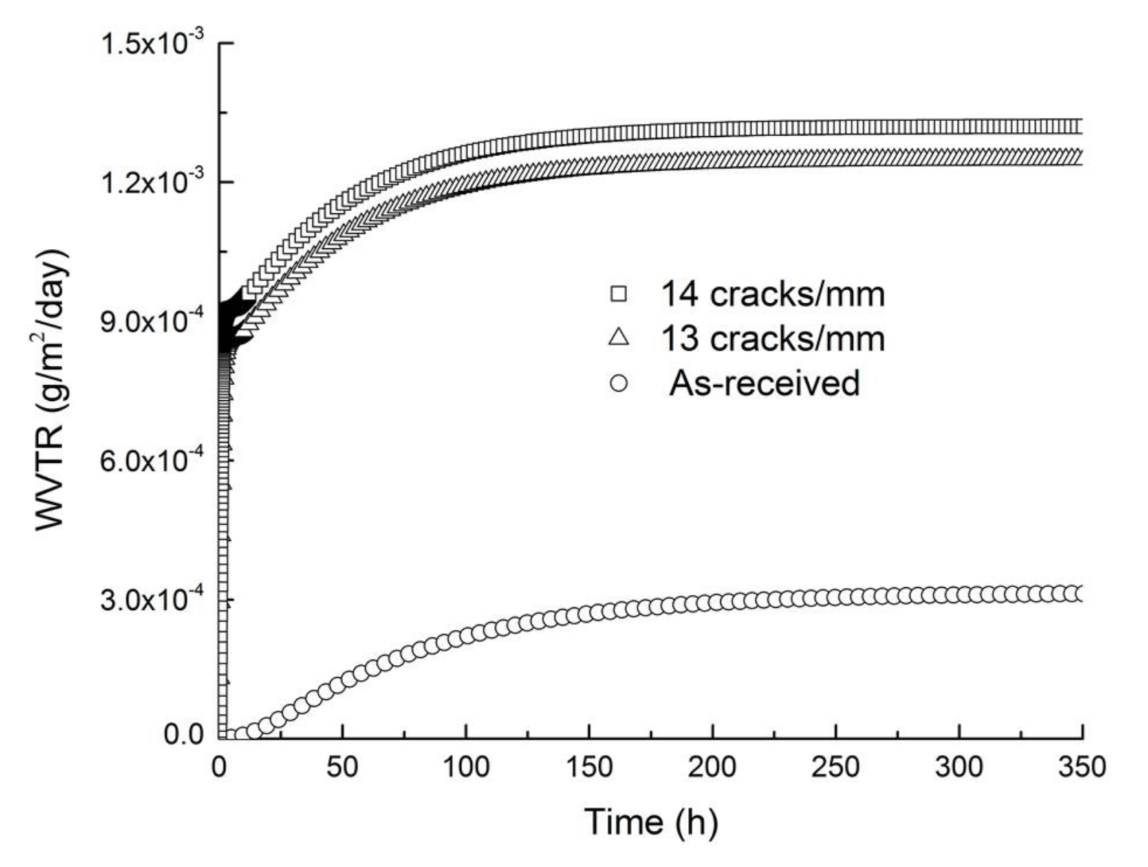
Figure 14.
Comparison of numerical and experimental results of WVTR value for the intact and damaged barrier thin films.
Figure 14.
Comparison of numerical and experimental results of WVTR value for the intact and damaged barrier thin films.

© 2018 by the authors. Licensee MDPI, Basel, Switzerland. This article is an open access article distributed under the terms and conditions of the Creative Commons Attribution (CC BY) license (http://creativecommons.org/licenses/by/4.0/).
Share and Cite
MDPI and ACS Style
Lu, H.-I.; Tran, D.-P.; Lin, C.-K.; To, B.-D. Effects of Long-Term Static Bending Deformation on a Barrier Thin Film for Flexible Organic Optoelectronic Devices. Coatings 2018, 8, 127. https://doi.org/10.3390/coatings8040127
AMA Style
Lu H-I, Tran D-P, Lin C-K, To B-D. Effects of Long-Term Static Bending Deformation on a Barrier Thin Film for Flexible Organic Optoelectronic Devices. Coatings. 2018; 8(4):127. https://doi.org/10.3390/coatings8040127
Chicago/Turabian StyleLu, Hung-I, Dinh-Phuc Tran, Chih-Kuang Lin, and Bao-Dong To. 2018. "Effects of Long-Term Static Bending Deformation on a Barrier Thin Film for Flexible Organic Optoelectronic Devices" Coatings 8, no. 4: 127. https://doi.org/10.3390/coatings8040127
Note that from the first issue of 2016, this journal uses article numbers instead of page numbers. See further details here.