Tube Inner Coating of Non-Conductive Films by Pulsed Reactive Coaxial Magnetron Plasma with Outer Anode

1
Graduate School of Engineering, Nagasaki University, 1-14, Bunkyo, Nagasaki 852-8521, Japan
2
GEOMATEC Co., Ltd., 51, Kinsei, Kannari, Kurihara, Miyagi 989-5164, Japan
*
Author to whom correspondence should be addressed.
Coatings 2018, 8(3), 115; https://doi.org/10.3390/coatings8030115
Submission received: 20 February 2018
/
Revised: 7 March 2018
/
Accepted: 19 March 2018
/
Published: 20 March 2018
Abstract
:The double-ended coaxial magnetron pulsed plasma (DCMPP) method with auxiliary outer anode was introduced in order to achieve the uniform coating of non-conductive thin films on the inner walls of insulator tubes. In this study, titanium (Ti) was employed as a cathode (sputtering target), and a glass tube was used as a substrate. In an argon (Ar) and oxygen (O2) gas mixture, magnetron plasma was generated. Oxygen gas was introduced to deposit a titanium oxide (TiO2) film. A comparison between films coated with and without an auxiliary outer anode was made. As a result, it was clearly shown that the DCMPP method using an auxiliary outer anode enhanced the uniformity of the deposited non-conductive film compared to the conventional DCMPP method. Moreover, the optimum conditions under which the thin TiO2 film was deposited on the inner wall of the glass tube were revealed. From the results, it was supposed that the auxiliary outer anode contributed to the uniformity of the distributions of deposited negative charge on the non-conductive film and consequently the electric field and the plasma density uniform.
1. Introduction
Narrow tubes are widely used in the industry for many applications such as the delivery of gas, water, cooling substances, etc. [1]. Enhancement of their properties in terms of corrosion and wear resistance is constantly required for these tubes. Therefore, it is indispensable to improve the attributes of the inner walls of such tubes. In this respect, several investigations have been performed [2,3,4,5,6,7,8,9,10]. Fujiyama et al. proposed coaxial magnetron pulsed plasma (CMPP) and double-ended coaxial magnetron pulsed plasma (DCMPP) methods for coating the inner walls of narrow tubes with the aid of the extended anode effect [11]. The extended anode effect is useful for the coating of conductive films inside insulator tubes, because the deposited film plays the role of an anode [11]. However, the extended anode effect cannot be used for insulator tube coatings of non-conductive or high resistivity films, because electrons charge up the tube inner walls and prevent plasma from spreading along the tube, as reported in our previous article [12]. Therefore, new methods for the uniform coating of non-conductive or high resistivity films on the inner walls of insulator tubes are required.
In this study we developed a new method introducing a grounded aluminum foil which covered the outside of the glass tube to work as an auxiliary outer anode in the DCMPP method.
2. Materials and Methods
2.1. Experimental Apparatus
The experimental apparatus for tube inner coating by double-ended coaxial magnetron pulsed plasmas (DCMPP) is shown in Figure 1.
A long cylindrical vacuum chamber, 1300 mm in length and 320 mm in inner diameter, was used and a water-cooled solenoidal coil was arranged coaxially around the chamber to generate a magnetic field, as shown in Figure 1a. The anode consisted of stainless steel (SUS) ring electrodes positioned at both ends of the tube, as shown in Figure 1b. The glass tube was 19 mm in outer diameter, 16.5 mm in inner diameter, and 500 mm in length. The part of the glass tube to be coated was only 435 mm in the middle of the tube, because the uncoated parts at both edges were covered with SUS ring anodes. The minimum discharge gap was 6.75 mm, as shown in Figure 1b. The glass tube was completely wrapped with a grounded aluminum foil from the outside, as shown in Figure 1c. This aluminum foil plays the role of an auxiliary outer anode, which enhances the axial uniformity of the deposited film thickness, as discussed later. A long fine cathode (a titanium rod 3 mm in diameter) was positioned at the center of the glass tube.
The coating was performed by applying pulsed voltage between the anode and cathode under the following experimental conditions: Magnetic flux density at 833 G, gas pressure at 1 Pa, mass flow rate of Ar at 100, 90, 80, 70, 60 or 50 SCCM. The pulsed power was generated with a pulse generator (Advanced Energy, Pinnacle Plus+ 10 kW (325–800 V dc), Advanced Energy Industries, Inc., Fort Collins, CO, USA). Oxygen gas was used to obtain non-conductive films, so the fraction of O2 was varied under a constant fraction of Ar. There were openings in the substrate holder to let the gas in. An axial strong magnetic field (833 G) was applied in order to make the breakdown easier in a narrow tube under low-pressure conditions. The magnetron effect confines the electrons near the target, and increases the probability of collisions between the electrons, ions, and atoms [13]. Consequently, pulsed discharge is generated between the long fine cathode and the grounded anode. The applied magnetic-flux density was calculated from the current of the solenoid coil. In this study, we applied the frequency of 100 kHz. The applied power, duty cycle, and sputtering time were set at 300 W, 55%, and 2 min (15 s × 8), respectively. We also performed the coating without the outer anode to clarify the effect of the outer anode.
In order to evaluate the thickness of the coated films, a flat glass substrate test piece (435 mm in length, 5 mm in width, and 0.7 mm in thickness) was inserted inside the tube. The flat substrate was marked by a magic pen at several positions. The mark prevents coating and creates a step change in the film thickness at the positions marked. We evaluated the thickness of the coatings by measuring the height of the step change at the corresponding position with a surface profilometer (Dektak 150, Veeco Instruments, Inc., Oyster Bay, NY, USA).
In order to measure the resistivity together with the film thickness, the flat substrate was cut into several pieces at the points that were marked by the magic pen. Then, the resistance was measured and the resistivity was calculated from the measured resistance.
2.2. Electrical Characterization
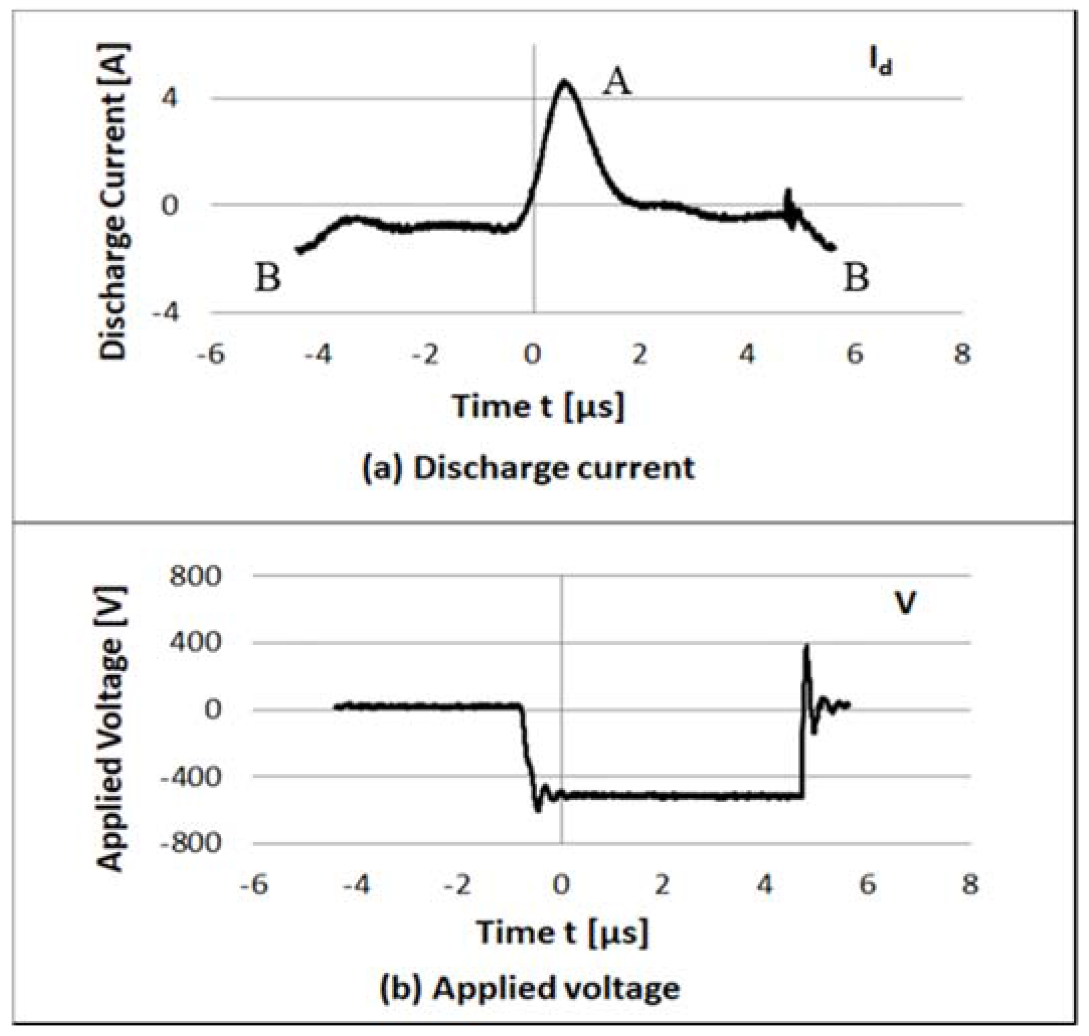
Figure 2 shows the typical voltage and current waveforms. The current waveform was measured with a current probe (TBS1102B, Tektronix, Inc., Beaverton, OR, USA) and an oscilloscope (P6021A, Tektronix, Inc., Beaverton, OR, USA). The positive current pulse (A in the figure) corresponds to the discharge current. On the other hand, the negative current pulse (B in the figure) is supposed to be a current due to the space charge in the gap, which is driven by the inverse electric field caused by the charge accumulated on the film surface. The duration of the inverse current was 1–2 μs. Then, the off-time necessary for the refreshment is supposed to be at least 1–2 μs.
Figure 3 shows the voltage and the current characteristics as a function of the pulsed power frequency, where the power was set at 300 W. A high frequency is better for increasing the discharge current. Consequently, we chose the frequency of 100 kHz at 300 W of input power, and the duty cycle and the sputtering time were set at 55% and 2 min (15 s × 8), respectively. We also performed the coating without the outer anode to clarify the effect of the outer anode.
3. Results
3.1. Coating of Non-Conductive Films by DCMPP
Figure 4 shows the relationship between the thickness of the coated film and the fraction of O2 in the case without an auxiliary outer anode. This graph shows that the coated film thickness decreases with increase of the fraction of O2 in the gas mixture.
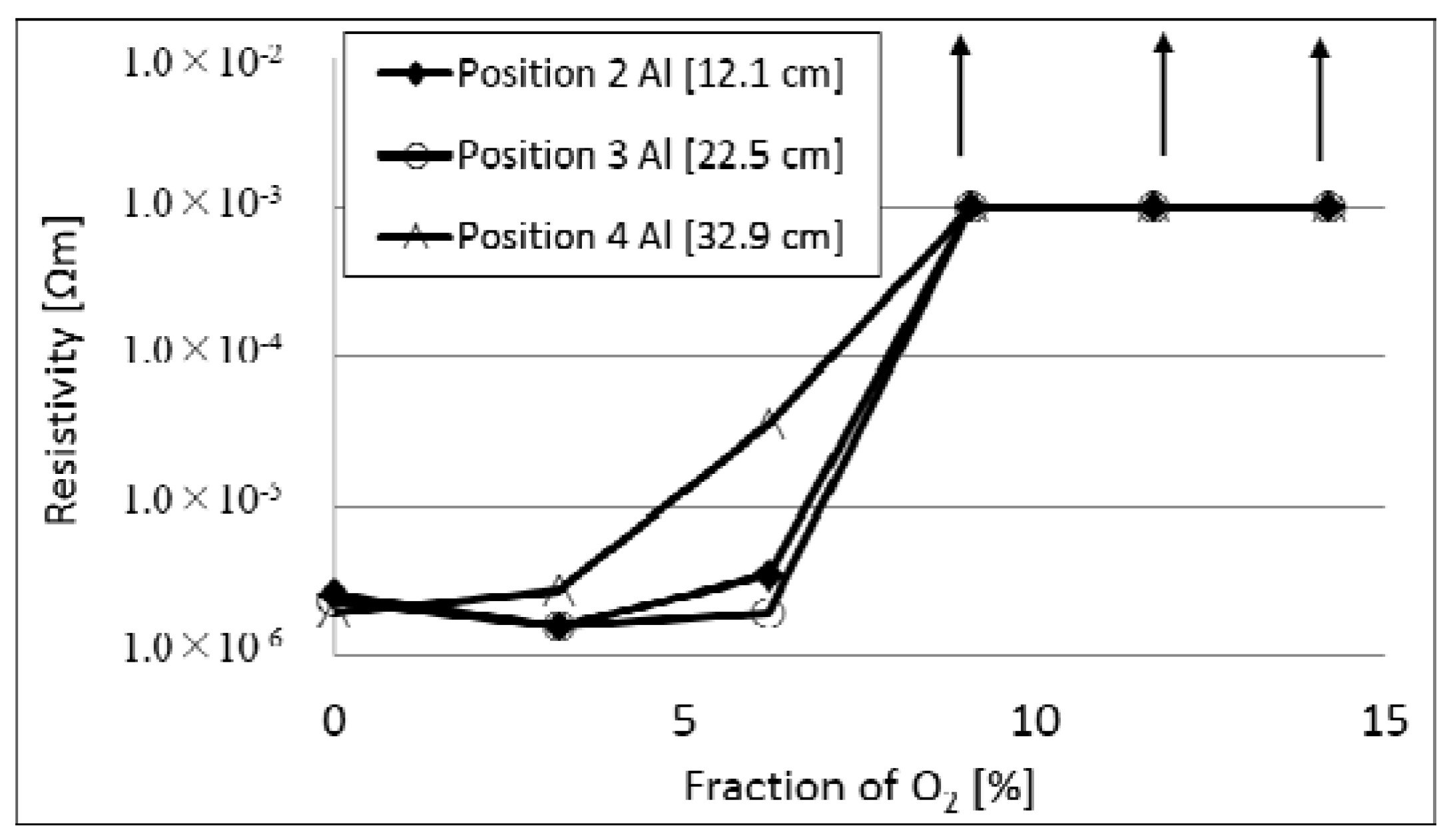
Figure 5 shows the relationship between the resistivity of the coated film and the fraction of O2. This graph indicates that the resistivity increased with the fraction of O2, and the property of the deposited film changed from metallic Ti to TiO2 at 9.1% of the fraction of O2. Under that condition, a film with relatively high resistivity (more than 10−3 Ω m) was produced. The increase of the fraction of O2 leads to the production of negative ions. When the coated film is conductive, the deposited film plays the role of an anode to spread plasma along the tube and the ions are neutralized through the conductive film. On the other hand, when the coated film is non-conductive, the ions deposit on the insulator glass and on the non-conductive film. Thus, the charge accumulation of the surface of the film depends on the resistivity of the film. In the case of a non-conductive or high resistive film, the major parts of the ions are deposited around the ring anodes and the electric field in the tube is affected by the deposited charges. Consequently, the plasma density was supposed to be reduced and the film became thinner compared to the cases of the fraction of O2 less than 9.1%, as shown in Figure 5.
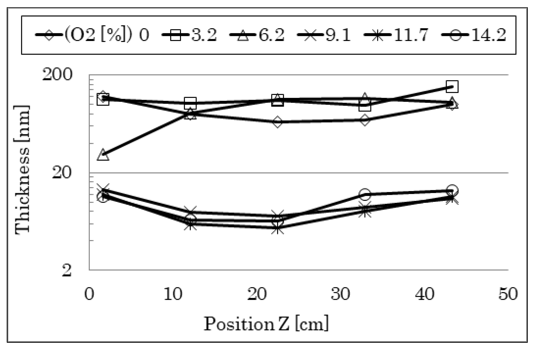
Figure 6 shows the distribution of the thickness of the coated film as a parameter of the fraction of O2 in the case without an outer anode. Three types of the distributions are recognized: an almost flat distribution at a low fraction of O2, a convex shape distribution at a middle fraction of O2, and a concave shape distribution at a high fraction of O2. The thickness of the deposited film decreased with the fraction of O2. This phenomenon can be attributed to the plasma density distribution affected by the change of the electric field distribution along the tube due to the change of the coated film resistivity.
3.2. Coating of Non-Conductive Films by DCMPP with an Outer Anode
Figure 7 shows the thickness distributions as a parameter of the fraction of O2 in the case with an outer anode. The results reinforce the findings in Figure 6. Higher resistivity of the coated film leads to the production of a thinner film. Figure 8 shows the relationship between the resistivity of the coated film and the fraction of O2 in the case with the Al outer anode. This graph indicates that the resistivity increased with the fraction of O2, and the property of the deposited film changed from metallic Ti to TiO2 at 9.1% of the fraction of O2. The criterion of the fraction of O2 for the coating of non-conductive film was around 9.1%. The films in Figure 7 seem to have better thickness profiles for high fractions of O2.
3.3. Uniformity of Non-Conductive Film with and without an Outer Anode
Figure 9 shows the comparison of the uniformity of the film thickness between the cases with and without an outer anode. The uniformity was evaluated by normalizing the film thickness by the average thickness. The error bars show the maximum and the minimum thicknesses normalized by the average thickness. Figure 9a shows the case without an outer anode and Figure 9b shows the case with an outer anode. The film was smooth in both cases at a fraction of O2 lower than 3.2% compared with a high fraction. On the other hand, the uniformity was better for the case with an outer anode compared with the case without an outer anode when the fraction was higher than 9.1%. The uniformity became improved with the outer anode at high fractions of O2. The electron density was supposed to decrease as the fraction of O2 increased because the electrons attached to the O2 molecules. This can be attributed to the production of negative ions which accumulated on the inner wall of the glass tube. In addition, the electron energy decreased owing to the collisions with O2 molecules. Consequently, the plasma density and the deposition rate were reduced.
From the above observations, using an auxiliary outer anode improved the axial uniformity of the deposited film thickness, and the validity of the suggested method in this study was made clear.
4. Discussion
Effect of the Outer Anode on Film Coating with DCMPP
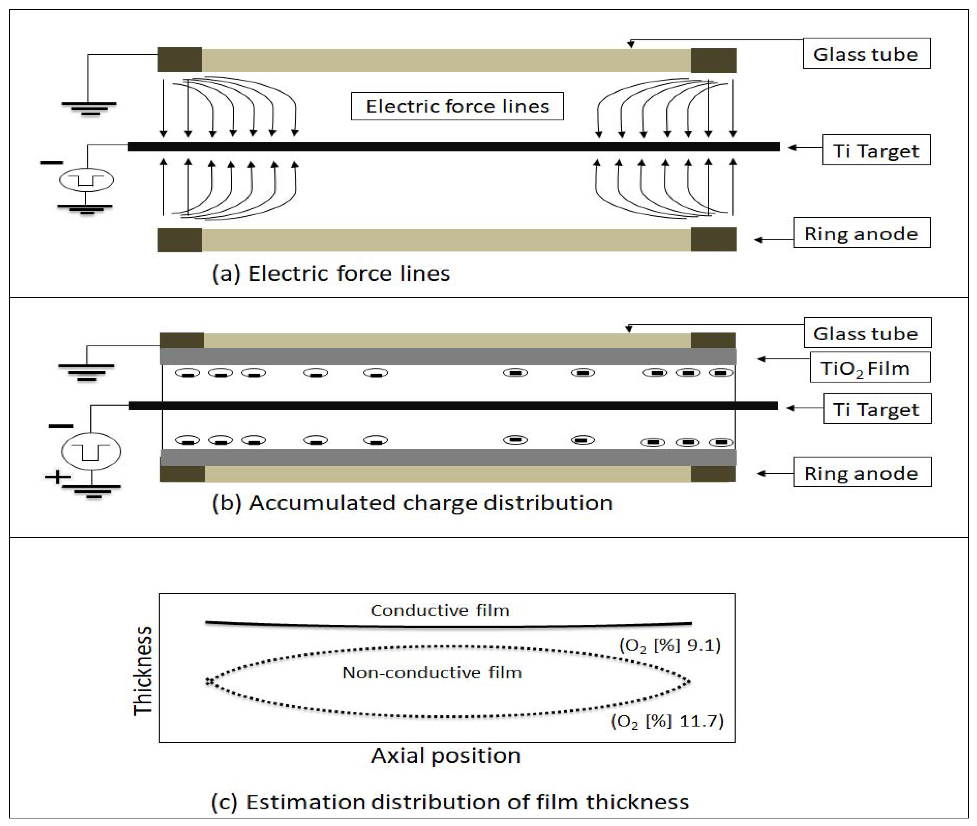
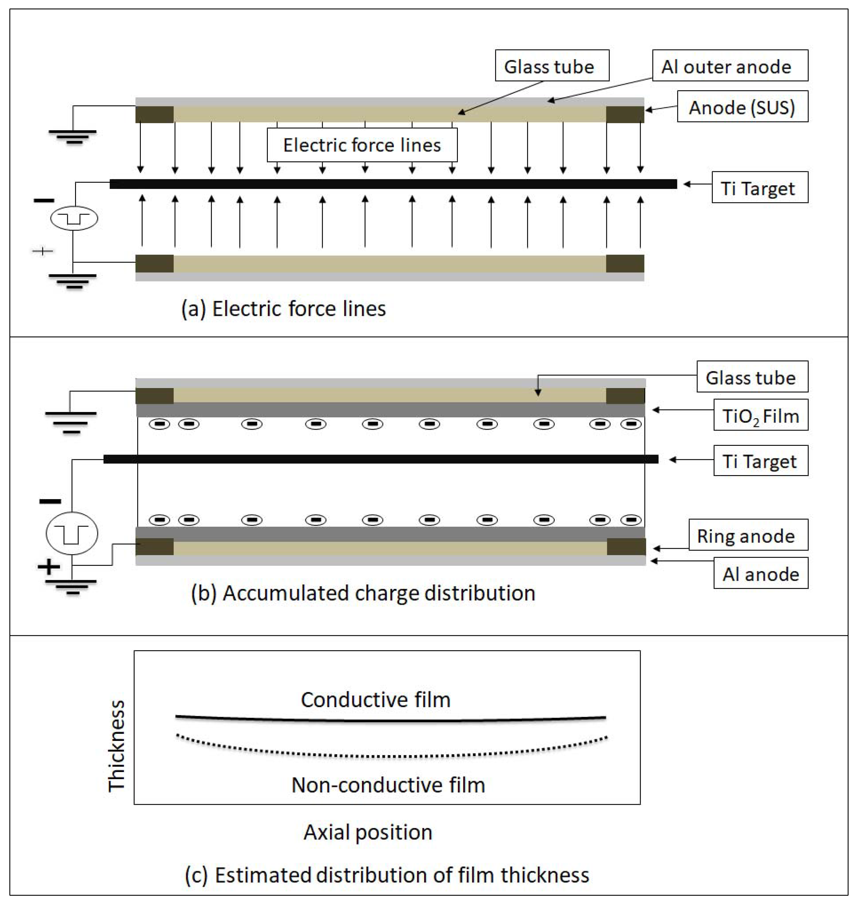
Figure 10 shows the characteristics of the DCMPP systems without using the auxiliary outer anode. Figure 10a shows a schematic representation of the electric force lines around the glass tube. The plasma density can be estimated from the electric field distribution and is supposed to be higher in both edges of the glass tube than in the middle. Figure 10b shows the expected electric charge distribution on the glass tube coated by a non-conductive film. This figure illustrates the accumulation of negative charges on the inner walls of the glass tube during the voltage pulse. Figure 10c demonstrates an estimation of the film thickness distribution in the case of a high resistance film. The deposited film was supposed to be thicker at both edges of the glass tube owing to the high plasma density. However, the density of charge accumulation, which is also higher compared with the middle of the tube, decreases the electric field and consequently reduces the plasma density. In addition, the resputtering of the film can be considered around the anode. The resputtering phenomenon happens due to the bombardment of negative ions on surface of the deposited film, and consequently reduces the film thickness. Since the electric field is stronger at both edges of the glass tube, the likelihood for negative ions to gain enough energy for resputtering is higher at both edges of the glass tube. These phenomena have a role in reducing the thickness, and the thickness distribution is thus represented as the dashed line shown in Figure 10c.
Figure 11 shows the characteristics of the DCMPP systems with the auxiliary outer anode. Figure 11a shows a schematic representation of the electric force lines around the glass tube. The plasma density estimated from the electric field distribution is supposed to be almost uniform. Figure 11b shows the expected electric charges distribution around the glass tube coated by a non-conductive film. Then, the distribution of the electric charge is also supposed to be uniform. Although the deposited charge decreases the electric field, the effect is expected to be uniform. Figure 11c shows an estimation of the film thickness distribution in the case of a high resistance film deposited with an outer anode. Since the uniform plasma density makes the film thickness uniform, the thickness distribution is depicted as the solid line shown in Figure 11c. The effect of the deposited charge, which reduces the plasma density, is also considered. When this effect is taken into account, the thickness distribution is depicted as the dashed line shown in Figure 11c.
As mentioned above, an outer auxiliary anode is expected to improve the thickness uniformity of a non-conductive coating on an inner surface of glass tube. Therefore, we synthesized the inner coating of a non-conductive film with a DCMPP system using an outer auxiliary anode.
5. Conclusions
The double-ended coaxial magnetron pulsed plasma (DCMPP) method with an auxiliary outer anode was introduced in order to achieve a uniform coating of non-conductive thin films on the inner walls of insulator tubes. A comparison between films coated with and without an auxiliary outer anode was made for various fractions of O2. As a result, it was clearly shown that use of an auxiliary outer anode with the DCMPP method improved the uniformity in the thickness of the deposited non-conductive TiO2 film compared to the use of DCMPP without an auxiliary outer anode. Moreover, it was revealed that the property of the deposited film changed from metallic Ti to TiO2 at the fraction of O2 around 9.1%. From the results, it was supposed that the auxiliary outer anode contributed to the uniformity of the distributions of the deposited negative charge on the non-conductive film, the electric field, and the plasma density.
Acknowledgments
The authors would like to thank H. Fukunaga for his valuable scientific help as well as for the financial support for the first author during several research internships. Many thanks GEOMATEC Co. Ltd. for several research internships and for the financial support for the first author’s transportation between Nagasaki University and the internship venue. Many thanks to K. Sakata and M. Kato for the technical help. The authors would also like to thank Y. Matsuda for his valuable scientific help. Finally, many thanks to T. Yamashita for his valuable scientific help.
Author Contributions
Hiroshi Fujiyama and Hiroyuki Sugawara conceived and designed the experiments; Musab Timan Idriss Gasab and Takemi Sato performed the experiments; Musab Timan Idriss Gasab and Hiroshi Fujiyama analyzed the data; Musab Timan Idriss Gasab and Hiroshi Fujiyama wrote the paper.
Conflicts of Interest
The authors declare no conflict of interest.
References
- Ohta, H.; Inoue, K.; Yamada, Y.; Yoshida, S.; Fujiyama, H.; Ishikura, S. Microgravity flow boiling in a transparent tube. In Proceedings of the 4th ASME-JSME Thermal Engineering Joint Conference, Maui, HI, USA, 19–24 March 1995; p. 547. [Google Scholar]
- Sheward, J.A. The coating of internal surfaces by PVD techniques. Surf. Coat. Technol. 1992, 297, 54–55. [Google Scholar]
- Hytry, R.; Moller, W.; Wilhelm, R.; Keudell, A.V. Moving-coil waveguide discharge for inner coating of metal tubes. J. Vac. Sci. Technol. 1993, 11, 2508–2517. [Google Scholar] [CrossRef]
- Ensinger, W. An apparatus for sputter coating the inner walls of tubes. Rev. Sci. Instrum. 1996, 67, 318–321. [Google Scholar] [CrossRef]
- Ensinger, W. Corrosion and wear protection of tube inner walls by ion beam sputter coating. Surf. Coat. Technol. 1996, 438, 86–87. [Google Scholar] [CrossRef]
- Schumacher, A.; Frech, G.; Wolf, G.K. A novel method for inside-coating of tubes and hollow cylinders by ion beam sputtering. Surf. Coat. Technol. 1997, 89, 258–261. [Google Scholar] [CrossRef]
- Fujiyama, H.; Tokitu, Y.; Uchikawa, Y.; Kuwahara, K.; Miyake, K.; Kuwahara, K.; Doi, A. Ceramics inner coating of narrow tubes by a coaxial magnetron pulsed plasma. Surf. Coat. Technol. 1998, 98, 1467–1472. [Google Scholar] [CrossRef]
- Uchikawa, Y.; Sugimoto, S.; Kuwahara, K.; Fujiyama, H.; Kuwahara, H. Titanium coating of the inner of a 1 m long narrow tube by double-ended anode coaxial magnetron-pulsed plasmas. Surf. Coat. Technol. 1999, 112, 185–188. [Google Scholar] [CrossRef]
- Xue, D.; Chen, Y.; Ling, G.; Liu, K.; Chen, C.; Zhang, G. Preparation of aluminide coatings on the inner surface of tubes by heat treatment of Al coatings electrodeposited from an ionic liquid. Fusion Eng. Des. 2015, 101, 128–133. [Google Scholar] [CrossRef]
- Ueda, M.; da Silva, A.R.; Pillaca, E.J.; Mariano, S.F.; Oliveira, R.M.; Rossi, J.O.; Lepienski, C.M.; Pichon, L. New method of plasma immersion ion implantation and also deposition of industrial components using tubular fixture and plasma generated inside the tube by high voltage pulses. Rev. Sci. Instrum. 2016, 87, 013902. [Google Scholar] [CrossRef] [PubMed]
- Sugimoto, S.; Uchikawa, Y.; Kuwahara, K.; Fujiyama, H.; Kuwahara, H. Extended Anode Effect in Coaxial Magnetron Pulsed Plasmas for Coating the Inside Surface of Narrow Tubes. Jpn. J. Appl. Phys. 1999, 38, 4342–4345. [Google Scholar] [CrossRef]
- Gasab, M.T.I.; Sugawara, H.; Sakata, K.; Fujiyama, H. Extended anode effect for tube inner coating of non-conductive ceramics by pulsed coaxial magnetron plasma. Mater. Sci. Appl. 2018, 9, 1–10. [Google Scholar] [CrossRef]
- Kelly, P.J.; Arnell, R.D. Magnetron sputtering: A review of recent developments and applications. Vacuum 2000, 56, 159–172. [Google Scholar] [CrossRef]
Figure 1.
Experimental apparatus: (a) overall setup; (b) details of the edge anode; and (c) details of the outer anode. The white parts indicate the glass tube and the black parts at the edge of the glass tube represent the ring anodes.
Figure 1.
Experimental apparatus: (a) overall setup; (b) details of the edge anode; and (c) details of the outer anode. The white parts indicate the glass tube and the black parts at the edge of the glass tube represent the ring anodes.
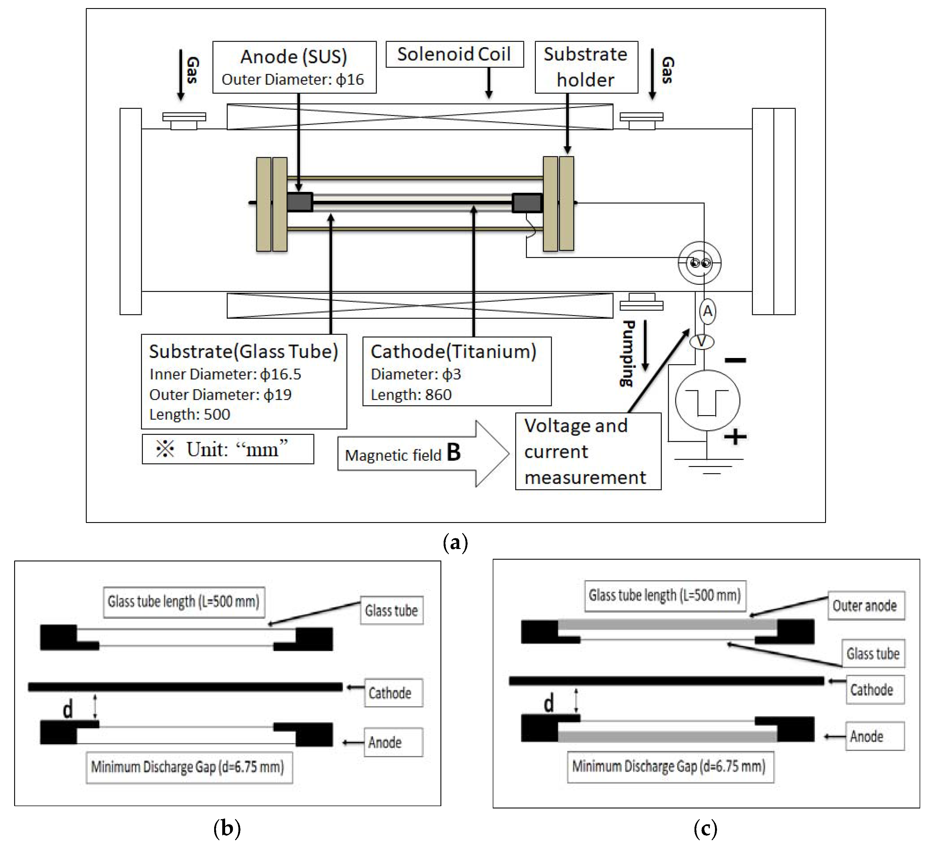
Figure 2.
Examples of the voltage and current waveforms at a frequency of 100 kHz in the case without the Al outer anode (the fraction of O2 is 6.2%). (a) Discharge current; and (b) applied voltage.
Figure 2.
Examples of the voltage and current waveforms at a frequency of 100 kHz in the case without the Al outer anode (the fraction of O2 is 6.2%). (a) Discharge current; and (b) applied voltage.

Figure 3.
Voltage and current characteristics as a function of frequency in the case without the Al outer anode (the fraction of O2 is 11.7%).
Figure 3.
Voltage and current characteristics as a function of frequency in the case without the Al outer anode (the fraction of O2 is 11.7%).
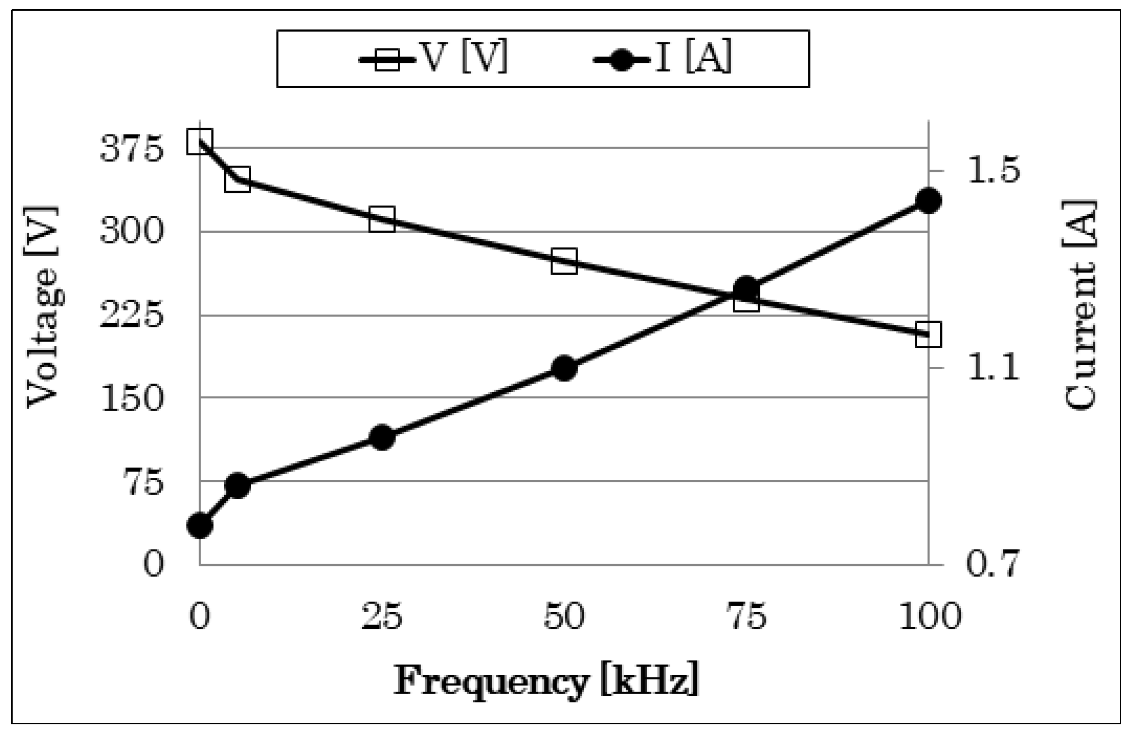
Figure 4.
Relation between the film thickness and the fraction of O2 (%) in the case without the Al auxiliary outer anode at the axial positions of 22.5 and 43.3 cm from the edge of the glass tube.
Figure 4.
Relation between the film thickness and the fraction of O2 (%) in the case without the Al auxiliary outer anode at the axial positions of 22.5 and 43.3 cm from the edge of the glass tube.
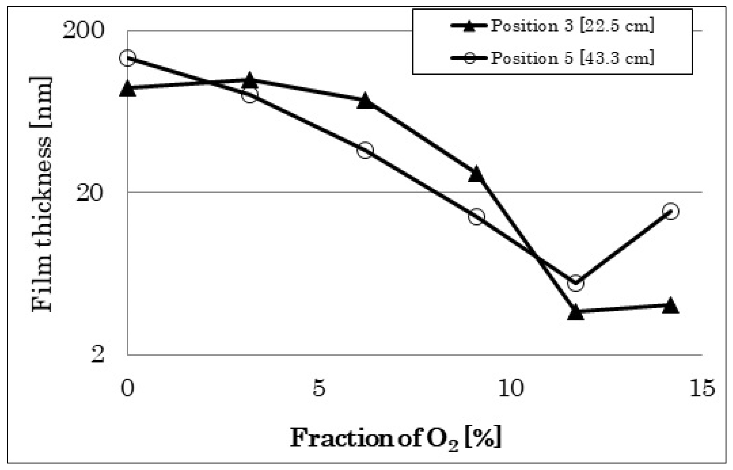
Figure 5.
Relation between the resistivity and the fraction of O2 (%) in the case without the Al outer anode at different positions.
Figure 5.
Relation between the resistivity and the fraction of O2 (%) in the case without the Al outer anode at different positions.
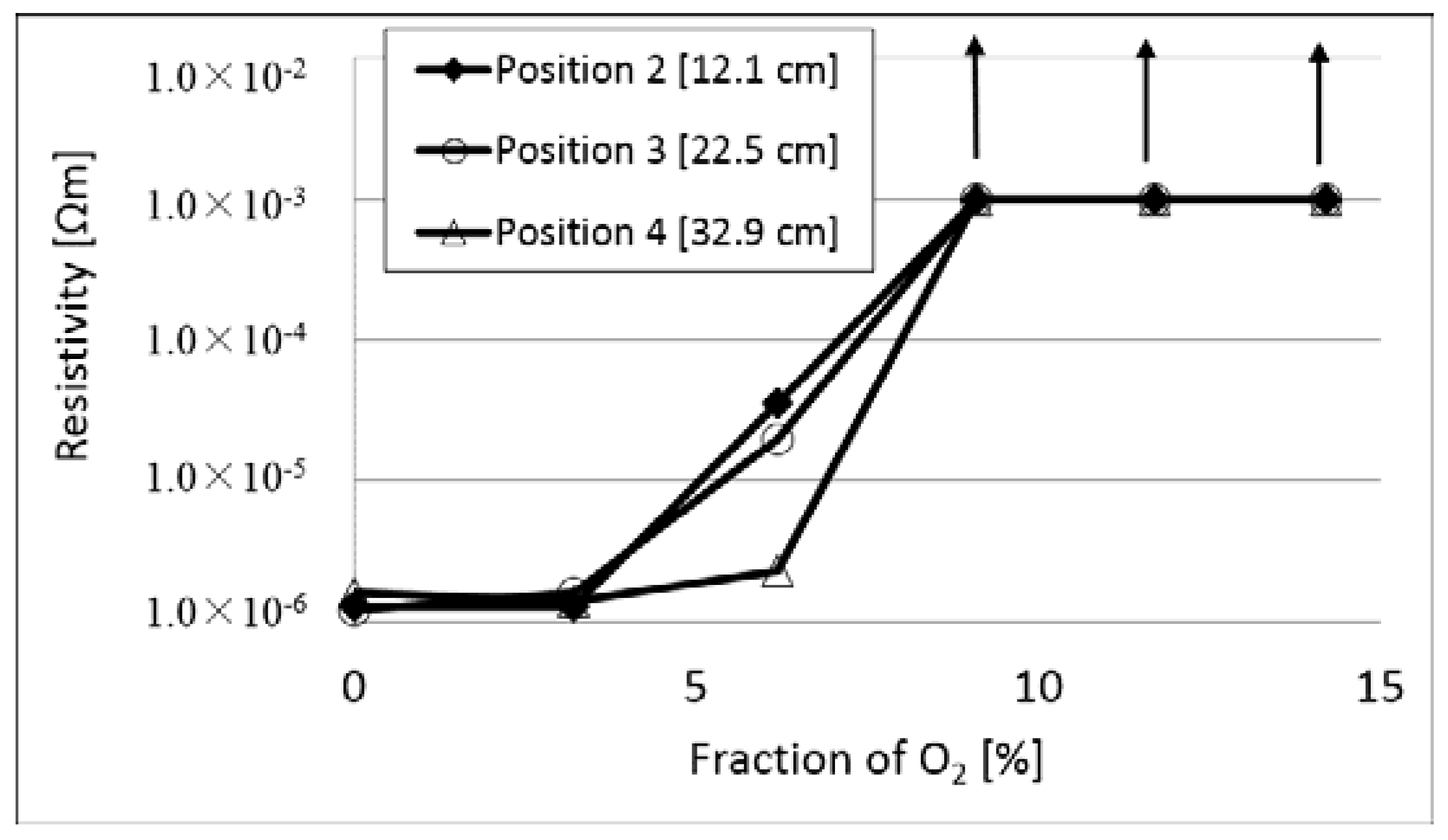
Figure 6.
Distribution of the film thickness along the axial position at different fractions of O2 (%) in the case without the Al outer anode.
Figure 6.
Distribution of the film thickness along the axial position at different fractions of O2 (%) in the case without the Al outer anode.
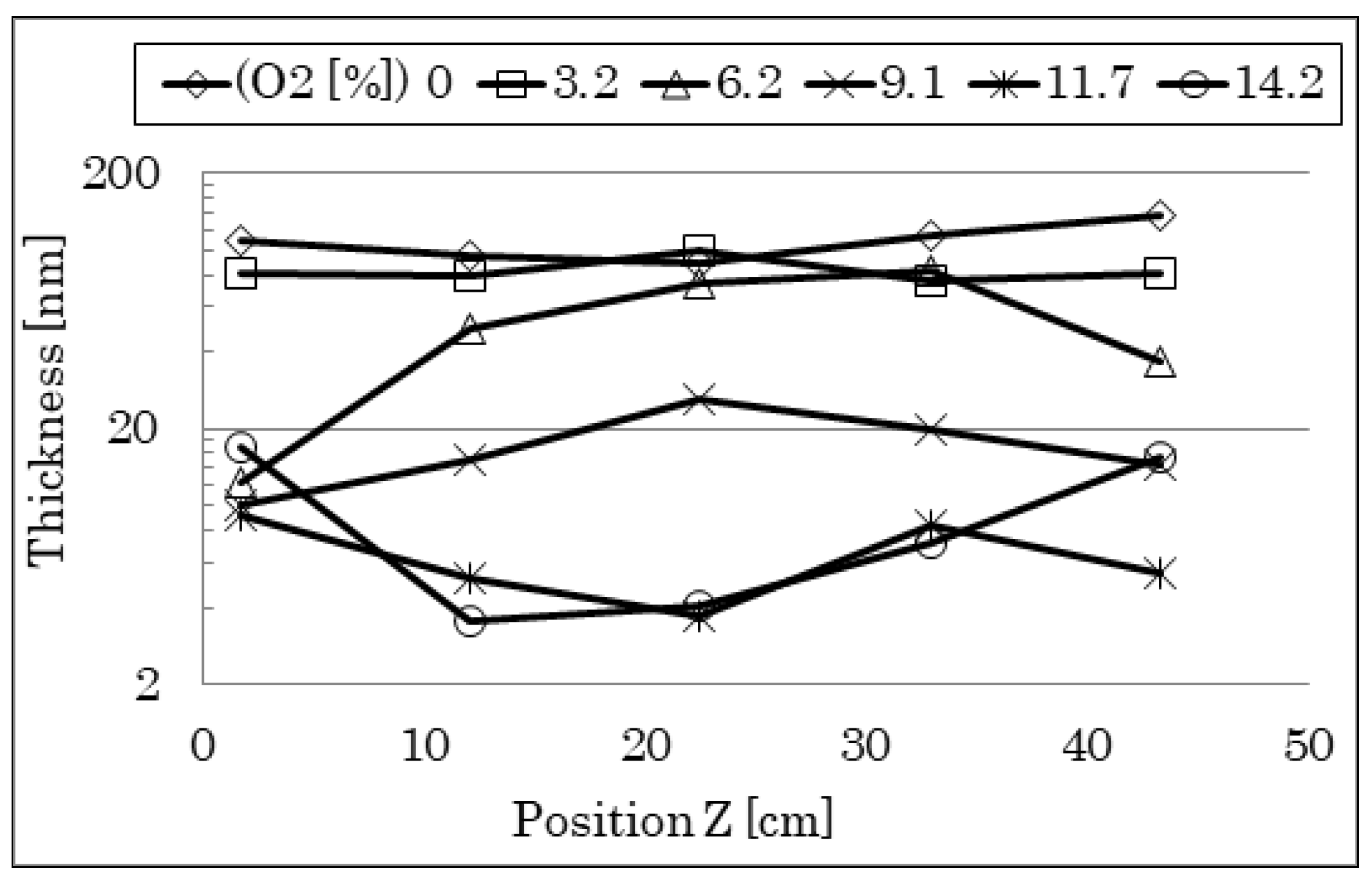
Figure 7.
Distributions of the film thickness along the axial position at different fraction of O2 (%) in the case with the Al outer anode.
Figure 7.
Distributions of the film thickness along the axial position at different fraction of O2 (%) in the case with the Al outer anode.

Figure 8.
Relation between the resistivity and the fraction of O2 (%) at different positions in the case with the Al outer anode.
Figure 8.
Relation between the resistivity and the fraction of O2 (%) at different positions in the case with the Al outer anode.

Figure 9.
Normalized thickness as a function of fraction of O2 in the case (a) without the Al outer anode; and (b) with the Al outer anode.
Figure 9.
Normalized thickness as a function of fraction of O2 in the case (a) without the Al outer anode; and (b) with the Al outer anode.
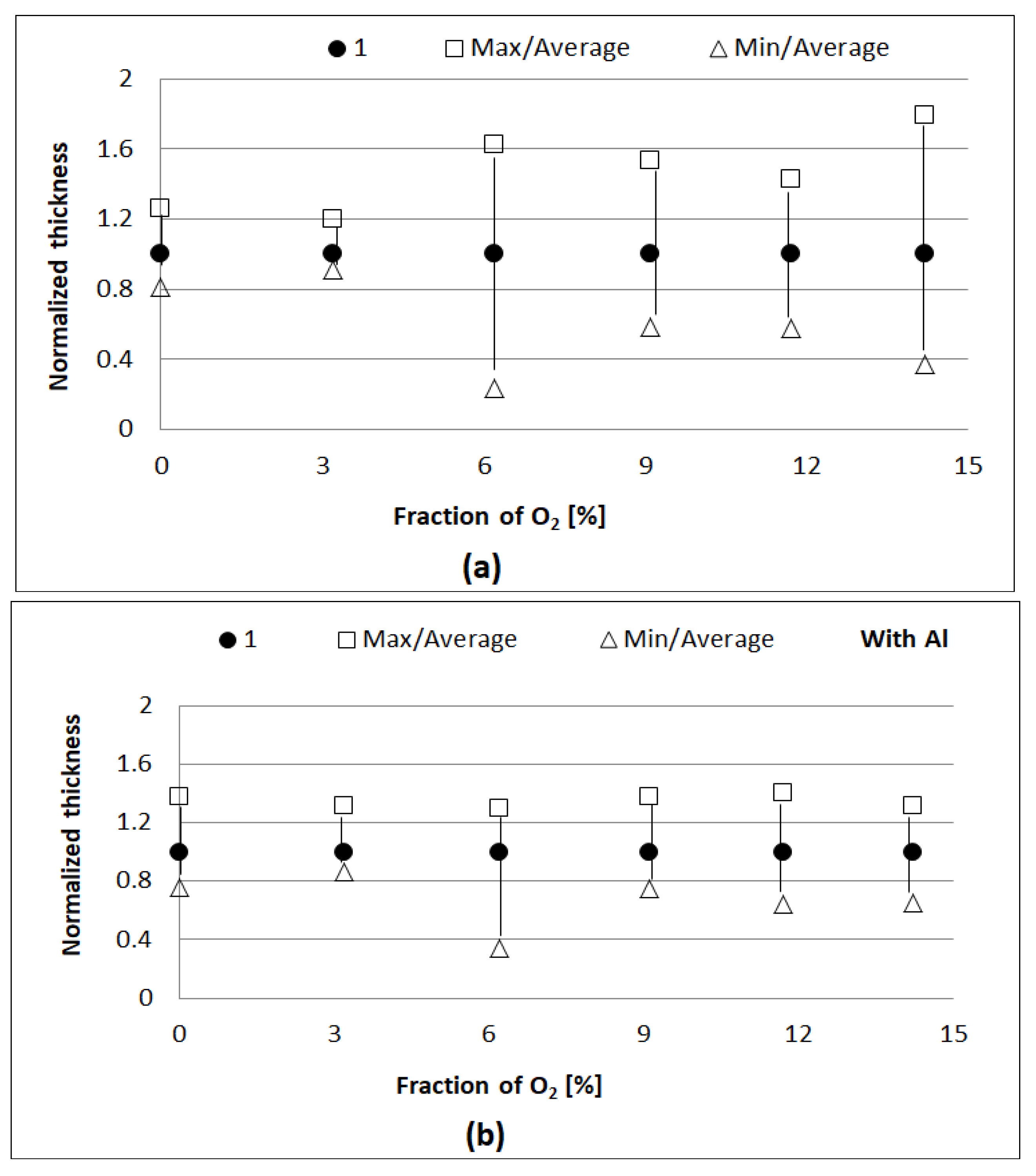
Figure 10.
Schematic representation of the electric force lines, electric charges distribution, and estimation of the film thickness distribution in the case without using the Al outer anode. (a) A schematic representation of the electric force lines around the glass tube; (b) accumulated charge distribution around the glass tube; and (c) an estimation of the film thickness distribution in the case of a high resistance film.

Figure 11.
Schematic representation of the electric force lines, electric charges distribution, and estimation of the film thickness distribution in the case with the Al outer anode. (a) A schematic representation of the electric force lines around the glass tube; (b) accumulated charge distribution around the glass tube; and (c) an estimation of the film thickness distribution in the case of a high resistance film.
© 2018 by the authors. Licensee MDPI, Basel, Switzerland. This article is an open access article distributed under the terms and conditions of the Creative Commons Attribution (CC BY) license (http://creativecommons.org/licenses/by/4.0/).
Share and Cite
MDPI and ACS Style
Gasab, M.T.I.; Sugawara, H.; Sato, T.; Fujiyama, H. Tube Inner Coating of Non-Conductive Films by Pulsed Reactive Coaxial Magnetron Plasma with Outer Anode. Coatings 2018, 8, 115. https://doi.org/10.3390/coatings8030115
AMA Style
Gasab MTI, Sugawara H, Sato T, Fujiyama H. Tube Inner Coating of Non-Conductive Films by Pulsed Reactive Coaxial Magnetron Plasma with Outer Anode. Coatings. 2018; 8(3):115. https://doi.org/10.3390/coatings8030115
Chicago/Turabian StyleGasab, Musab Timan Idriss, Hiroyuki Sugawara, Takemi Sato, and Hiroshi Fujiyama. 2018. "Tube Inner Coating of Non-Conductive Films by Pulsed Reactive Coaxial Magnetron Plasma with Outer Anode" Coatings 8, no. 3: 115. https://doi.org/10.3390/coatings8030115
Note that from the first issue of 2016, this journal uses article numbers instead of page numbers. See further details here.